SERVICE MANUAL FOR M35&36; CHASSIS
SERVICE MANUAL FOR M35&36; CHASSIS
SERVICE MANUAL FOR M35&36; CHASSIS

You also want an ePaper? Increase the reach of your titles
YUMPU automatically turns print PDFs into web optimized ePapers that Google loves.
TCL<br />
Chassis M35&<strong>36</strong> Service Manual<br />
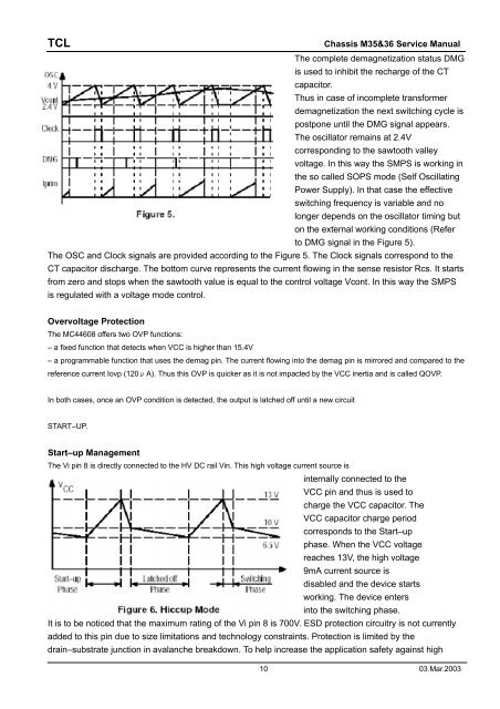
The complete demagnetization status DMG<br />
is used to inhibit the recharge of the CT<br />
capacitor.<br />
Thus in case of incomplete transformer<br />
demagnetization the next switching cycle is<br />
postpone until the DMG signal appears.<br />
The oscillator remains at 2.4V<br />
corresponding to the sawtooth valley<br />
voltage. In this way the SMPS is working in<br />
the so called SOPS mode (Self Oscillating<br />
Power Supply). In that case the effective<br />
switching frequency is variable and no<br />
longer depends on the oscillator timing but<br />
on the external working conditions (Refer<br />
to DMG signal in the Figure 5).<br />
The OSC and Clock signals are provided according to the Figure 5. The Clock signals correspond to the<br />
CT capacitor discharge. The bottom curve represents the current flowing in the sense resistor Rcs. It starts<br />
from zero and stops when the sawtooth value is equal to the control voltage Vcont. In this way the SMPS<br />
is regulated with a voltage mode control.<br />
Overvoltage Protection<br />
The MC44608 offers two OVP functions:<br />
– a fixed function that detects when VCC is higher than 15.4V<br />
– a programmable function that uses the demag pin. The current flowing into the demag pin is mirrored and compared to the<br />
reference current Iovp (120 A). Thus this OVP is quicker as it is not impacted by the VCC inertia and is called QOVP.<br />
In both cases, once an OVP condition is detected, the output is latched off until a new circuit<br />
START–UP.<br />
Start–up Management<br />
The Vi pin 8 is directly connected to the HV DC rail Vin. This high voltage current source is<br />
internally connected to the<br />
VCC pin and thus is used to<br />
charge the VCC capacitor. The<br />
VCC capacitor charge period<br />
corresponds to the Start–up<br />
phase. When the VCC voltage<br />
reaches 13V, the high voltage<br />
9mA current source is<br />
disabled and the device starts<br />
working. The device enters<br />
into the switching phase.<br />
It is to be noticed that the maximum rating of the Vi pin 8 is 700V. ESD protection circuitry is not currently<br />
added to this pin due to size limitations and technology constraints. Protection is limited by the<br />
drain–substrate junction in avalanche breakdown. To help increase the application safety against high<br />
10 03.Mar.2003