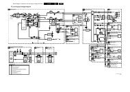
SERVICE MANUAL FOR M35&36; CHASSIS
SERVICE MANUAL FOR M35&36; CHASSIS
SERVICE MANUAL FOR M35&36; CHASSIS

Create successful ePaper yourself
Turn your PDF publications into a flip-book with our unique Google optimized e-Paper software.
TCL<br />
Chassis M35&<strong>36</strong> Service Manual<br />
<strong>SERVICE</strong> <strong>MANUAL</strong> <strong>FOR</strong> M35&<strong>36</strong> <strong>CHASSIS</strong><br />
PART I. Servicing Precautions<br />
When working, the unit is with ultra high voltage about 25KV inside. So, to avoid the risk of electric shock,<br />
be careful to adjust the chassis!<br />
1. Only qualified personnel should perform service procedures.<br />
2. All specification must be met over line voltage ranger of 160V AC to 240V AC 50Hz/60Hz.<br />
3. Do not operate in WET/DAMP conditions.<br />
4. Portions of the power supply board are hot ground. The remaining boards are cold ground.<br />
5. Discharge of CRT anode should be done only to CRT ground strap.<br />
6. When fuse blow, ensure to replace a fuse with the same type and specification.<br />
7. Keep the wires away from the components with high temperature or high voltage.<br />
8. When replacing the resister with high power, keep it over the PCB about 10mm.<br />
9. The CRT anode high voltage has been adjusted and set in the factory. When repairing the chassis, do<br />
not make the high voltage exceed 27.5KV (The beam current is 0uA). Generally, the high voltage is set on<br />
25.5KV 1.5KV (The beam current is 700uA).<br />
* The values of parameters above are for information only.<br />
10. Before return the fixed unit, do check all the covering of wires to ensure that not fold or not short with<br />
any metal components. Check the entire protection units, such as control knobs, rear cabinet & front panel,<br />
insulation resister & capacitor, mechanical insulators and so on.<br />
11. There are some mechanical and electrical parts associating with safety (EMC) features (Generally<br />
related to high voltage or high temperature or electric shock), these features cannot be found out from the<br />
outside. When replace these components, perhaps the voltage and power suit the requirements, but<br />
efficient X-ray protection may not be provided. All these components are marked with in the schematic<br />
diagram. When replace these, you’d better look up the components listed in this manual. If the component<br />
you replaced not has the same safety (EMC) performance, harmful X-ray may be produced.<br />
1 03.Mar.2003
TCL<br />
Part -Product Specification<br />
1. Ambient conditions:<br />
1.1 Ambient temperatures:<br />
a. Operating: -10 ~ +40<br />
b. Storage: -15 ~ +45<br />
Chassis M35&<strong>36</strong> Service Manual<br />
1.2 Humidity<br />
a. Operation: < 80%<br />
b. Storage: < 90%<br />
1.3 Air pressure: 86kpa ~ 106kpa<br />
2. Chassis Specification<br />
2.1 MCU/Video/Teletext IC: VCT 3831A Super one chip IC<br />
2.2 System<br />
[ M35:PAL-DK.1 M<strong>36</strong>:PAL-DK/BG ]<br />
SECAM DK/BG<br />
Receiving channels<br />
CATV 470MHz<br />
Scanning lines and frequencies 525/625 lines 15.625kHz/15.75kHz 50/60Hz<br />
Color sub-carrier<br />
4.433MHz/3.579MHz<br />
2.3 IF:picture 38.9MHz sound 5.5MHz/6.0MHz/6.5MHz<br />
2.4 Power Consumption:120W (M<strong>36</strong> ) 70W (M35)<br />
2.5 Power Supply: AC 220V 45-55Hz<br />
2.6 Audio Output Power(7%THD): 29” >6W+6W (M<strong>36</strong>) 21” 3W+3W (M35)<br />
2.7 Aerial Input Impedance:75 Unbalanced Din Jack Ant.Input<br />
2.8 Product Safety Requirement: CE<br />
2.9 Product EMC/EMI Requirement: CE<br />
3. Basic Feature of Controller<br />
3.1 Channel Tuning Method: Voltage Synthesizer<br />
3.2 Presettable Program:100 Programs<br />
3.3 Tuning for VHF and UHF Bands: Auto/Manual/Fine Tuning<br />
3.4 Picture and Sound Adjustment<br />
Bright, Contrast, Color and Volume Control;<br />
Tint Control(NTSC);<br />
2 03.Mar.2003
TCL<br />
[Treble, Bass, Balance Control (M<strong>36</strong> have these, but M35 haven’t)]<br />
Sharpness Control<br />
Chassis M35&<strong>36</strong> Service Manual<br />
3.5 OSD<br />
General Features(Volume, Brightness, Contrast, Color, Program, Band, Auto Search, Manual, Tune,<br />
Muting, AV And Sleep Timer)<br />
Stereo Dual Language<br />
Four Sound Effect Indicator<br />
3.6 Sleep Timer:15MIN<br />
3.7 Remote Effective Distance:8m<br />
3.8 Construction of Front Panel<br />
Main Power Switch<br />
Remote Sensor<br />
Menu Select<br />
TV/AV Select<br />
Standby Indicator<br />
Program Volume UP/DOWN<br />
RCA Socket (Side)<br />
3.9 Construction of Rear Panel<br />
75 Aerial Terminal<br />
RCA Socket (AV Input Only)<br />
Scart Socket<br />
S.VHS Input<br />
Specification Scart RCA<br />
Video input 75 1V p-p 1V p-p<br />
Audio input 10k (R+L) 0.5V rms 0.5V rms<br />
Video output 75 1V p-p 1V p-p<br />
Audio output 1k (R+L) 0.5V rms 0.5V rms<br />
RGB input 75 0.7V p-p<br />
Audio line output 1k 1V p-p<br />
• Design and specifications are subject to change without prior notice for the purpose of performance<br />
improvement.<br />
• This specification is only for your reference.<br />
3 03.Mar.2003
TCL<br />
Part<br />
-Brief Introduction On Chassis<br />
Chassis M35&<strong>36</strong> Service Manual<br />
RF IN<br />
TUNER<br />
Z101(Z102)<br />
SAWFILTER<br />
IF AMP<br />
M52760<br />
Key<br />
Sensor<br />
X-TAL<br />
20.25MHz<br />
IF<br />
IC 201<br />
VCT3831A<br />
Video AMP<br />
And Sense<br />
SCART<br />
AV2 IN<br />
I 2 C BUS<br />
I 2 C BUS<br />
24C016<br />
E 2 PROM<br />
Q401,Q402<br />
H DRIVE<br />
IC301<br />
V-OUTPUT<br />
TDA8172<br />
Hi-POT<br />
H-OUTPUT<br />
FBT(T401)<br />
IC1001<br />
MSP3415G<br />
IC601<br />
TDA7057<br />
AC220V<br />
DT801<br />
IC801<br />
MC44608<br />
Q801<br />
T802<br />
POWER<br />
TRANSISTOR<br />
B +,<br />
16V<br />
33V<br />
9V,5V,3.3V<br />
M35 and M<strong>36</strong> use a high-quality singlechip IC VCT3831A as TV processors . It is a combo IC with TV<br />
process unit and CPU inside. The follows are the operation theory with example of M35.<br />
1. Tuning section<br />
This section mainly consists of tuner and its accessory circuits. VCT3831A will control the band switching<br />
via Pin7 and Pin 10. (See table 1)<br />
PIN 7 PIN 10 BAND<br />
VCT3831A sends out a 5Vp-p VT signal with pulse-width<br />
High level Low level VHF-L modulation from Pin6. This signal is amplified with phase<br />
Low level High level VHF-H inversion by Q210, and changed to a 33Vp-p pulse signal with<br />
High level High level UHF pulse-width modulation. R255, C242, R256, C101, R101 and<br />
C102 compose a triple integral circuit, which is in charge of changing the 33Vp-p PWM signal to a DC<br />
tuning voltage which is variable from 0V to 33V. The tuner will select the corresponding channel according<br />
to the tuning voltage. If the sync signal and AFT signal cannot be inputted to the control section of<br />
VCT3831A, the auto tuning function will be invalidated. During the auto tuning process, the CVBS out from<br />
IC101, which is in charge of IF amplifying and demodulation, enter VCT3831A from Pin19. This CVBS will<br />
be treated by sync separation circuit inside VCT3831A and sends out a H-sync signal to the control unit of<br />
VCT3831A. If the H sync is detected by the control unit of VCT3831A, CPU will consider that a channel will<br />
be locked soon. So the tuning speed will slower automatically. On the other hand, an AFT signal out from<br />
Pin2 of IC101 enter VCT3831A from Pin9 of it. The control unit of VCT3831A will detect the accuracy of<br />
tuning according to the voltage of AFT signal.<br />
Bythis way, tuning with high accuracy can be achieved. And the corresponding tuning data will be stored in<br />
memory IC. Then the auto tuning process will go on and auto stop at the end (VFH-L VFH-H UHF) .<br />
2. VIF section<br />
The tuner sends out IF signal from Pin IF. This signal is amplified about 20db by Q101. Having passed the<br />
4 03.Mar.2003
TCL<br />
Chassis M35&<strong>36</strong> Service Manual<br />
SAWZ101 and Z101A, the IF signal is inputted into IC101 from Pin4-5 (VIF input) and Pin7 (SIF input). The<br />
VIF signal pass the video amplifier and video detector and is changed to CVBS. And IC101 sends out<br />
CVBS from Pin18 of itself. Having passed Q104 and Q105 and the trapper network consisted by L102,<br />
Z104 and Z105, CVBS is divide into two way. One enter IC201 from Pin19. And another pass Q903 and<br />
arrive the video output terminal of TV.<br />
IC101 sends out QIF signal from Pin13 of itself. QIF signal enters the sound process circuit which is mainly<br />
consisted by IC1001. A 38.9MHz VCO coil is connected with Pin 15 and 16 of IC101. By adjusting the<br />
magnetic core of T101, the AFT curve can match the standard. IF AGC delay signal comes out from Pin1<br />
of IC101, and goes to tuner for high frequency signal amplifying with auto-gain control.<br />
3. Sound process section<br />
M35/<strong>36</strong> chassis adopts MSP3415G made by Micronas also as sound process IC. This IC can process the<br />
stereo signal and NICAM signal.<br />
The QIF signal pass a high pass filter network consisted by C1024, C1024A and L1102, and enter IC1001<br />
from Pin47. This QIF signal is changed to sound signal via amplitude-limit amplifier and frequency<br />
discrimination circuit and sound deemphasis circuit inside the sound process IC. On the other hand, the<br />
two way audio signals from audio input terminal enter IC1001 from Pin42/44 and Pin39/40, they and the<br />
TV sound signal will be switched by IC1001. IC1001 selects one way sound signal from these three ways<br />
and divide it into two ways: One way is from Pin 24/25 to the audio amplifier circuit which is mainly<br />
consisted by TDA7057AQ and to drive the speakers. Another way is from Pin30/31 to audio out terminal of<br />
TV. VCT3831A sends out the volume control signal via Pin64 to control the speakers volume.<br />
4. Video signal process section<br />
The video signal from sound IF filter circuit enter IC201 via Pin19, and pass a video amplifier inside of IC.<br />
Then the video signal is splitted into two ways, one way to the sync-separation circuit, another one to the<br />
clamp circuit, black strength circuit, luminance delay line, sharpness improvement circuit. Then this signal<br />
is done with matrix operation with the C signal, which is from the chroma process unit, in the matrix circuit.<br />
The finally result is IC201 output R/G/B signal to CRT board from Pin42/43/44 and to drive the CRT.<br />
Another video signal which come from video input terminal of TV, is switched by electrical switch inside<br />
IC201 and out from pin11 of IC201 as the video output signal to video output terminal.<br />
5. Chroma process section<br />
The chroma signal is separated from the video signal, which is from pin19 or pin20 or 21 (video input or TV<br />
video signal), after having passed a band/ high pass filter. Then the chroma signal is amplified by ACC<br />
circuit and splitted into two ways. One way goes to the demodulation unit and another way goes to the<br />
APC circuit to make the chroma subcarrier oscillator to generate reference subcarrier signal which is<br />
needed for sync demodulation, and to sent it to the demodulation unit. The R-Y and B-Y signal<br />
demodulated from chroma signal are sent to color system recognition circuit. Having passed the system<br />
recognition switch circuit, it goes to 1H delay line and other control circuit. Finally it goes to matrix circuit.<br />
The Y signal from luminance process unit will be done with matrix operation with R-Y and B-Y signal via<br />
matrix circuit. If the color system is NTSC, the TINT circuit is enabled. This TINT circuit is a phase shift<br />
circuit. It can change the phase of the reference subcarrier which is sent to APC circuit and to shift the<br />
APC output voltage, therefore , to change the oscillator frequency (phase) of chroma VCO. So the chroma<br />
will be changeable.<br />
5 03.Mar.2003
TCL<br />
Chassis M35&<strong>36</strong> Service Manual<br />
6. Vertical output section<br />
IC VCT3831A outputs vertical saw-tooth waveform from Pin33. It comes to pin1 of TDA8172 with DC<br />
coupling. And it is amplified by inner difference amplifier. Pin7 of TDA8172 is the same phase input<br />
terminal. R302 is DC offset resistances. In application to M35, pin7 of TDA8172 is connected with Pin34<br />
vert0. The amplified saw tooth-wave comes out from pin5 and make the deflect coil to generate the deflect<br />
current. R307 and C305 filtrate the inductive interference from the horizontal deflect coil. C307 is used to<br />
eliminate spurious oscillation generated by the deflect coil and distributed capacitance resonance. R312,<br />
R320 and accessory circuit are in charge of draw AC saw tooth wave out, and feedback to the input<br />
terminal of TDA8172 (pin1) to correct the linearity of horizontal scan. D302 and C301 make up of a voltage<br />
pump up circuit. TDA8172 output a vertical kickback impulse from pin6 to locate the OSD characters.<br />
7. Horizontal Output And FBT Section<br />
The processor outputs horizontal drive impulse from pin24 H-OUT. The drive impulse is done with voltage<br />
division by R268 and D401, and then comes to the base of the drive triode (Q401). C401 is used to<br />
eliminate the noise in the H drive impulse. T402 is a horizontal drive transformer. Q402 is a horizontal<br />
output triode with a damper inside. The deflect coil and the horizontal output triode have some resistance<br />
R while they are ducting. The resistance R will cause the non-linear distortion, which means that the right<br />
direction scanning speed of the electron beam becomes slower, and the right of the raster is compressed<br />
to generate distortion. We use a horizontal linear adjuster to compensate this kind of distortion. We use<br />
L402 as the H linear adjuster in horizontal scanning section of M35 chassis. R409, which is parallel<br />
connected with L402 and L401, is a despiking resistance for preventing the oscillation by compensating<br />
inductor and the stray capacitance. The linear adjuster is a transductor coil with a magnetic core inside. If<br />
the current, which pass the linear adjuster coil, increase to a certain value, the magnetic core becomes<br />
saturated to decrease the inductance of the linear adjustment inductor. If the +B is steady, the increase<br />
speed of Iy is faster to compensate the reducing of deflecting current by the resistance R mention above.<br />
We can adjust the magnetic core to change the inductance of the linear compensate inductor to adjust the<br />
H linearity.<br />
M<strong>36</strong> Block Diagram (Consult above M35 part for Brief Introduction on Chassis)<br />
RF IN<br />
TUNER<br />
Z101(Z102)<br />
SAWFILTER<br />
IF AMP<br />
M52760<br />
Key<br />
Sensor<br />
X-TAL<br />
20.25MHz<br />
IF<br />
IC 201<br />
VCT3831A<br />
Video AMP<br />
And Sense<br />
SCART<br />
AV2 IN<br />
I 2 C BUS<br />
I 2 C BUS<br />
24C16<br />
E 2 PROM<br />
Q401,Q402<br />
H DRIVE<br />
IC301<br />
V-OUTPUT<br />
TDA8172<br />
Hi-POT<br />
H-OUTPUT<br />
FBT(T401)<br />
IC901<br />
MSP3415G/MSP346CG<br />
IC602<br />
TDA8944<br />
AC220V<br />
DT801<br />
IC801<br />
MC44608<br />
Q801<br />
T802<br />
POWER<br />
TRANSISTOR<br />
B +,<br />
18V<br />
33V<br />
9V,5V,3.3V<br />
6 03.Mar.2003
TCL<br />
PART IV. IC Pin Description<br />
1. MC44608-High Voltage PWM Controller<br />
Chassis M35&<strong>36</strong> Service Manual<br />
Pin Name Description<br />
1 Demag<br />
2 Isense<br />
3<br />
Control<br />
Input<br />
The Demag pin offers 3 different functions: Zero voltage crossing detection (50mV), 24<br />
A current detection and 120 A current detection. The 24 A level is used to detect the<br />
secondary reconfiguration status and the 120 A level to detect an Over Voltage status<br />
called Quick OVP.<br />
The Current Sense pin senses the voltage developed on the series resistor inserted in<br />
the source of the power MOSFET. When Isense reaches 1V, the Driver output (pin 5) is<br />
disabled. This is known as the Over Current Protection function. A 200 A current source<br />
is flowing out of the pin 3 during the start–up phase and during the switching phase in<br />
case of the Pulsed Mode of<br />
operation. A resistor can be inserted between the sense resistor and the pin 3, thus a<br />
programmable peak current detection can be performed during the SMPS stand–by<br />
mode.<br />
A feedback current from the secondary side of the SMPS via the opto–coupler is<br />
injected into this pin. A resistor can be connected between this pin and GND to allow<br />
the programming of the Burst duty cycle during the Stand–by mode.<br />
4 Ground This pin is the ground of the primary side of the SMPS.<br />
5 Driver The current and slew rate capability of this pin are suited to drive Power MOSFETs.<br />
6 VCC<br />
This pin is the positive supply of the IC. The driver output gets disabled when the<br />
voltage becomes higher than 15V and the operating range is between 6.6V and 13V.<br />
An intermediate voltage level of 10V creates a disabling condition called Latched Off<br />
phase.<br />
7 This pin is to provide isolation between the Vi pin 8 and the VCC pin 6.<br />
8 Vi<br />
This pin can be directly connected to a 500V voltage source for start–up function of the<br />
IC. During the Start–up phase a 9 mA current source is internally delivered to the VCC<br />
pin 6 allowing a rapid charge of the VCC capacitor. As soon as the IC starts–up, this<br />
current source is disabled.<br />
7 03.Mar.2003
TCL<br />
Chassis M35&<strong>36</strong> Service Manual<br />
OPERATING DESCRIPTION<br />
Regulation<br />
The pin 3 senses the feedback current provided by the opto-coupler. During the switching phase the switch<br />
S2 is closed and the shunt regulator is accessible by the pin 3. The shunt regulator voltage is typically 5V.<br />
The dynamic resistance of the shunt regulator represented by the zener diode is 20 .<br />
The gain of the Control input is given on Figure 10 which shows the duty cycle as a function of the current<br />
injected into the pin 3.<br />
The maximum current sense threshold is fixed at 1V. The peak A 4KHz filter network is inserted<br />
between the shunt regulator and the<br />
PWM comparator to cancel the high<br />
frequency residual noise.<br />
The switch S3 is closed in Stand–by<br />
mode during the Latched Off Phase<br />
while the switch S2 remains open. (See<br />
section PULSED MODE DUTY<br />
CYCLE CONTROL).<br />
The resistor Rdpulsed (Rduty cycle<br />
burst) has no effect on the regulation<br />
process. This resistor is used to<br />
determine the burst duty cycle.<br />
PWM Latch<br />
The MC44608 works in voltage mode. The on–time is controlled by the PWM comparator that compares<br />
the oscillator sawtooth with the regulation block output.<br />
The PWM latch is initialized by the<br />
oscillator and is reset by the PWM<br />
comparator or by the current sense<br />
comparator in case of an over current.<br />
This configuration ensures that only a<br />
single pulse appears at the circuit<br />
output during an oscillator cycle.<br />
Current Sense<br />
The inductor current is converted to a<br />
positive voltage by inserting a ground<br />
reference sense resistor RSense in series<br />
with the power switch.<br />
The maximum current sense threshold is fixed at 1V. The peak current is given by the following equation:<br />
Ipkmax = 1/Rsense( ) (A)<br />
In stand–by mode, this current can be lowered as due to the activation of a 200 A current source:<br />
IpkMAX-STBY<br />
The current sense input consists of a filter (6k , 4pF) and of a leading edge blanking. Thanks to that, this<br />
pin is not sensitive to the power switch turn on noise and spikes and practically in most applications, no<br />
filtering network is required to sense the current.<br />
Finally, this pin is used:<br />
8 03.Mar.2003
TCL<br />
– as a protection against over currents (Isense > I)<br />
– as a reduction of the peak current during a Pulsed Mode switching phase.<br />
Chassis M35&<strong>36</strong> Service Manual<br />
The overcurrent propagation delay is reduced by producing a sharp output turn off (high slew rate).<br />
This results in an abrupt output turn off in the event of an over current and in the majority of the pulsed<br />
mode switching sequence.<br />
Demagnetization Section<br />
The MC44608 demagnetization<br />
detection consists of a<br />
comparator designed to compare<br />
the VCC winding voltage to a<br />
reference that is typically equal<br />
to 50mV.<br />
This reference is chosen low to<br />
increase effectiveness of the<br />
demagnetization detection even<br />
during start–up.<br />
A latch is incorporated to turn<br />
the demagnetization block<br />
output into a low level as soon<br />
as a voltage less than 50 mV is<br />
detected, and to keep it in this<br />
state until a new pulse is<br />
generated on the output. This<br />
avoids any ringing on the input<br />
signal which may alter the<br />
demagnetization detection.<br />
For a higher safety, the<br />
demagnetization block output is<br />
also directly connected to the<br />
output, which is disabled during the demagnetization phase.<br />
The demagnetization pin is also used for the quick programmable OVP. In fact, the demagnetization input<br />
current is sensed so that the circuit output is latched off when this current is detected as higher than 120<br />
A.<br />
This function can be inhibited by grounding it but in this case, the quick and programmable OVP is also<br />
disabled.<br />
Oscillator<br />
The MC44608 contains a fixed frequency oscillator. It is built around a fixed value capacitor CT succesively<br />
charged and discharged by two distinct current sources ICH and IDCH. The window comparator senses<br />
the CT voltage value and activates the sources when the voltage is reaching the 2.4V/4V levels.<br />
9 03.Mar.2003
TCL<br />
Chassis M35&<strong>36</strong> Service Manual<br />
The complete demagnetization status DMG<br />
is used to inhibit the recharge of the CT<br />
capacitor.<br />
Thus in case of incomplete transformer<br />
demagnetization the next switching cycle is<br />
postpone until the DMG signal appears.<br />
The oscillator remains at 2.4V<br />
corresponding to the sawtooth valley<br />
voltage. In this way the SMPS is working in<br />
the so called SOPS mode (Self Oscillating<br />
Power Supply). In that case the effective<br />
switching frequency is variable and no<br />
longer depends on the oscillator timing but<br />
on the external working conditions (Refer<br />
to DMG signal in the Figure 5).<br />
The OSC and Clock signals are provided according to the Figure 5. The Clock signals correspond to the<br />
CT capacitor discharge. The bottom curve represents the current flowing in the sense resistor Rcs. It starts<br />
from zero and stops when the sawtooth value is equal to the control voltage Vcont. In this way the SMPS<br />
is regulated with a voltage mode control.<br />
Overvoltage Protection<br />
The MC44608 offers two OVP functions:<br />
– a fixed function that detects when VCC is higher than 15.4V<br />
– a programmable function that uses the demag pin. The current flowing into the demag pin is mirrored and compared to the<br />
reference current Iovp (120 A). Thus this OVP is quicker as it is not impacted by the VCC inertia and is called QOVP.<br />
In both cases, once an OVP condition is detected, the output is latched off until a new circuit<br />
START–UP.<br />
Start–up Management<br />
The Vi pin 8 is directly connected to the HV DC rail Vin. This high voltage current source is<br />
internally connected to the<br />
VCC pin and thus is used to<br />
charge the VCC capacitor. The<br />
VCC capacitor charge period<br />
corresponds to the Start–up<br />
phase. When the VCC voltage<br />
reaches 13V, the high voltage<br />
9mA current source is<br />
disabled and the device starts<br />
working. The device enters<br />
into the switching phase.<br />
It is to be noticed that the maximum rating of the Vi pin 8 is 700V. ESD protection circuitry is not currently<br />
added to this pin due to size limitations and technology constraints. Protection is limited by the<br />
drain–substrate junction in avalanche breakdown. To help increase the application safety against high<br />
10 03.Mar.2003
TCL<br />
Chassis M35&<strong>36</strong> Service Manual<br />
voltage spike on that pin it is possible to insert a small wattage 1k series resistor between the Vin rail and<br />
pin 8.<br />
The Figure 6 shows the VCC voltage evolution in case of no external current source providing current into<br />
the VCC pin during the switching phase. This case can be encountered in SMPS when the self supply<br />
through an auxiliary winding is not present (strong overload on the SMPS output for example).<br />
The Figure16 also depicts this working configuration.<br />
In case of the hiccup mode, the duty cycle of the switching phase is in the range of 10%.<br />
Mode Transition<br />
The LW latch Figure 7 is the<br />
memory of the working<br />
status at the end of every<br />
switching sequence. Two<br />
different cases must be<br />
considered for the logic<br />
at the termination of the<br />
SWITCHING<br />
PHASE:<br />
1.No Over Current was observed<br />
2.An Over Current was observed<br />
These 2 cases are corresponding to the signal labeled NOC in case of “No Over Current” and “OC” in case<br />
of Over Current. So the effective working status at the end of the ON time memorized in LW corresponds<br />
to Q=1 for no over current and Q=0 for over current.<br />
This sequence is repeated during the Switching phase.<br />
Several events can occur:<br />
1. SMPS switch OFF<br />
2. SMPS output overload<br />
3. Transition from Normal to Pulsed Mode<br />
4. Transition from Pulsed Mode to Normal Mode<br />
1. SMPS SWITCH OFF<br />
When the mains is switched OFF, so long as the bulk electrolithic bulk capacitor provides energy to the<br />
SMPS, the controller remains in the switching phase. Then the peak current reaches its maximum peak<br />
value, the switching frequency decreases and all the secondary voltages are reduced. The VCC voltage is<br />
also reduced. When VCC is equal to 10V, the SMPS stops working.<br />
2. Overload<br />
In the hiccup mode the 3 distinct phases are described as follows (refer to Figure 6):<br />
The SWITCHING PHASE: The SMPS output is low and the regulation block reacts by increasing the ON<br />
time (dmax = 80%). The OC is reached at the end of every switching cycle. The LW latch (Figure 7) is<br />
reset before the VPWM signal appears. The SMPS output voltage is low. The VCC voltage cannot be<br />
maintained at a normal level as the auxiliary winding provides a voltage which is also reduced in a ratio<br />
similar to the one on the output (i.e. Vout nominal / Vout short–circuit). Consequently the VCC voltage is<br />
reduced at an operating rate given by the combination VCC capacitor value together with the ICC working<br />
consumption (3.2mA) according to the equation 2. When VCC crosses 10V the WORKING PHASE gets<br />
11 03.Mar.2003
TCL<br />
Chassis M35&<strong>36</strong> Service Manual<br />
terminated. The LW latch remains in the reset status.<br />
The LATCHED–OFF PHASE: The VCC capacitor voltage continues to drop. When it reaches 6.5V this<br />
phase is terminated. Its duration is governed by equation 3.<br />
The START–UP PHASE is reinitiated. The high voltage start–up current source (–ICC1 = 9mA) is activated<br />
and the MODE latch is reset. The VCC voltage ramps up according to the equation 1. When it reaches 13V,<br />
the IC enters into the SWITCHING PHASE.<br />
The NEXT SWITCHING PHASE: The high voltage current source is inhibited, the MODE latch (Q=0)<br />
activates the NORMAL mode of operation. Figure 2 shows that no current is injected out pin 2.<br />
The over current sense level corresponds to 1V.<br />
As long as the overload is present, this sequence repeats. The SWITCHING PHASE duty cycle is in the<br />
range of 10%.<br />
3. Transition from Normal to Pulsed Mode<br />
In this sequence the secondary side is reconfigured (refer to the typical application schematic). The high<br />
voltage output value becomes lower than the NORMAL mode regulated value. The TL431 shunt regulator<br />
is fully OFF. In the SMPS stand–by mode all the SMPS outputs are lowered except for the low voltage<br />
output that supply the wake–up circuit located at the isolated side of the power supply. In that mode the<br />
secondary regulation is performed by the zener diode connected in parallel to the TL431.<br />
The secondary reconfiguration status can be detected on the SMPS primary side by measuring the voltage<br />
level present on the auxiliary winding Laux. (Refer to the Demagnetization Section). In the reconfigured<br />
status, the Laux voltage is also reduced. The VCC self–powering is no longer possible thus the SMPS<br />
enters in a hiccup mode similar to the one described under the Overload condition.<br />
In the SMPS stand–by mode the 3 distinct phases are:<br />
The SWITCHING PHASE: Similar to the Overload mode. The current sense clamping level is reduced<br />
according to the equation of the current sense section. The C.S. clamping level depends on the power to<br />
be delivered to the load during the SMPS stand–by mode. Every switching sequence ON/OFF is<br />
terminated by an OC as long as the secondary Zener diode voltage has not been reached. When the<br />
Zener voltage is reached the ON cycle is terminated by a true PWM action. The proper SWITCHING<br />
PHASE termination must correspond to a NOC condition. The LW latch stores this NOC status.<br />
The LATCHED OFF PHASE: The MODE latch is set.<br />
The START–UP PHASE is similar to the Overload Mode. The MODE latch remains in its set status (Q=1).<br />
The SWITCHING PHASE: The Stand–by signal is validated and the 200 A is sourced out of the Current<br />
Sense pin 2.<br />
4. Transition from Stand–by to Normal<br />
The secondary reconfiguration is removed. The regulation on the low voltage secondary rail can no longer<br />
be achieved, thus at the end of the SWITCHING PHASE, no PWM condition can be encountered. The LW<br />
latch is reset.<br />
At the next WORKING PHASE a NORMAL mode status takes place.<br />
In order to become independent of the recovery time SWITCHING PHASE constant on the secondary side<br />
of the SMPS an additional reset input R2 is provided on the MODE latch. The condition Idemag
TCL<br />
Chassis M35&<strong>36</strong> Service Manual<br />
Pulsed Mode Duty Cycle Control<br />
During the sleep mode of the SMPS the switch S3 is closed and the control input pin 3 is connected to a<br />
4.6V voltage source thru a 500 resistor. The discharge rate of the VCC capacitor is given by ICC–latch<br />
(device consumption during the LATCHED OFF phase) in addition to the current drawn out of the pin 3.<br />
Connecting a resistor between the Pin 3 and GND (RDPULSED) a programmable current is drawn from<br />
the VCC through pin 3. The duration of the LATCHED OFF phase is impacted by the presence of the<br />
resistor RDPULSED. The equation 3 shows the relation to the pin 3 current.<br />
Pulsed Mode Phases<br />
Equations 1 through 8 define and predict the effective behavior during the PULSED MODE operation. The<br />
equations 6, 7, and 8 contain K, Y, and D factors. These factors are combinations of measured parameters.<br />
They appear in the parameter section “K factors for pulsed mode operation”. In equations 3 through 8 the<br />
pin 3 current is the current defined in the above section “Pulsed Mode Duty Cycle Control”.<br />
2. TDA8172 TV Vertical Deflection Output Circuit<br />
General Description<br />
The TDA8172 is a monolithic integrated circuit. It is a high efficiency power booster for direct driving of<br />
vertical windings of TV yokes. It is intended for use in Color and B&W television.<br />
Pin Connections (top view)<br />
Block Diagram<br />
13 03.Mar.2003
TCL<br />
3. TDA8944 2 7W stereo Bridge Tied Load (BTL) Audio Amplifier<br />
General Description<br />
Chassis M35&<strong>36</strong> Service Manual<br />
The TDA8944 is a dual-channel audio power amplifier with an output power of 2 7W at an 8 load<br />
and a 12V supply. The circuit contains two Bridge Tied Load (BTL) amplifiers with an all-NPN output<br />
stage and standby/mute logic. The TDA8944 comes in a 17-pins DIL-bent-SIL (DBS) power package.<br />
Features<br />
Few external components<br />
Fixed gain<br />
Standby and mute mode<br />
No on/off switching plops<br />
Low standby current<br />
High supply voltage ripple rejection<br />
Outputs short-circuit protected to ground, supply and across the load<br />
Thermally protected<br />
Printed-circuit board compatible.<br />
Block Diagram and Pin Configuration<br />
Pin Description<br />
No. Symbol Pin Description<br />
1 OUT1− 1 negative loudspeaker terminal 1<br />
2 GND1 2 ground channel 1<br />
3 VCC1 3 supply voltage channel 1<br />
4 OUT1+ 4 positive loudspeaker terminal 1<br />
5 n.c. 5 not connected<br />
6 IN1+ 6 positive input 1<br />
7 n.c. 7 not connected<br />
14 03.Mar.2003
TCL<br />
Chassis M35&<strong>36</strong> Service Manual<br />
No. Symbol Pin Description<br />
8 IN1− 8 negative input 1<br />
9 IN2− 9 negative input 2<br />
10 MODE 10 mode selection input (standby, mute, operating)<br />
11 SVR 11 half supply voltage decoupling (ripple rejection)<br />
12 IN2+ 12 positive input 2<br />
13 n.c. 13 not connected<br />
14 OUT2− 14 negative loudspeaker terminal 2<br />
15 GND2 15 ground channel 2<br />
16 VCC2 16 supply voltage channel 2<br />
17 OUT2+ 17 positive loudspeaker terminal 2<br />
Functional Description<br />
The TDA8944J is a stereo BTL audio power amplifier capable of delivering 2 × 7 W output power to an 8 Ω load<br />
at THD = 10%, using a 12 V power supply and an external heat sink. The voltage gain is fixed at 32 dB. With<br />
the three-level MODE input the device can be switched from ‘standby’ to ‘mute’ and to ‘operating’ mode. The<br />
TDA8944J outputs are protected by an internal thermal shutdown protection mechanism and a short-circuit<br />
protection.<br />
1 Input configuration<br />
The TDA8944J inputs can be driven symmetrical (floating) as well as asymmetrical. In the asymmetrical mode<br />
one input pin is connected via a capacitor to the signal ground which should be as close as possible to the SVR<br />
(electrolytic) capacitor ground. Note that the DC level of the input pins is half of the supply voltage VCC, so<br />
coupling capacitors for both pins are necessary.<br />
2 Power amplifier<br />
The power amplifier is a Bridge Tied Load (BTL) amplifier with an all-NPN output stage, capable of delivering a<br />
peak output current of 2 A.<br />
The BTL principle offers the following advantages:<br />
• Lower peak value of the supply current<br />
• The ripple frequency on the supply voltage is twice the signal frequency<br />
• No expensive DC-blocking capacitor<br />
• Good low frequency performance.<br />
3 Mode selection<br />
The TDA8944J has three functional modes, which can be selected by applying the proper DC voltage to pin<br />
MODE.<br />
Standby - In this mode the current consumption is very low and the outputs are floating. The device is in<br />
standby mode when (VCC − 0.5 V) < VMODE < VCC, or when the MODE pin is left floating (high impedance). The<br />
power consumption of the TDA8944J will be reduced to
TCL<br />
Chassis M35&<strong>36</strong> Service Manual<br />
Internal Circuitry<br />
No. Pin Symbol Equivalent Circuit<br />
1<br />
6 and 8<br />
IN1+ and IN1-<br />
12 and 9<br />
IN2+ and IN2-<br />
2<br />
1 and 4<br />
14 and 17<br />
OUT1- and OUT1+<br />
OUT2- and OUT2+<br />
3 10 MODE<br />
4 11 SVR<br />
16 03.Mar.2003
TCL<br />
Chassis M35&<strong>36</strong> Service Manual<br />
Application Information<br />
Application diagram.<br />
4. TDA8945 15 W mono Bridge Tied Load (BTL) audio amplifier<br />
General description<br />
The TDA8945S is a single-channel audio power amplifier with an output power of 15 W at an 8 Ω load and<br />
an 18 V supply. The circuit contains a Bridge Tied Load (BTL) amplifier with an all-NPN output stage and<br />
standby/mute logic. The TDA8945S comes in a 9-lead single in-line (SIL) power package.<br />
c<br />
c Features<br />
The same as TDA8944.<br />
17 03.Mar.2003
TCL<br />
Block Diagram and Pin Configuration<br />
Chassis M35&<strong>36</strong> Service Manual<br />
Pin Description<br />
No. Symbol Pin Description<br />
1 OUT− 1 negative loudspeaker terminal<br />
2 VCC 2 supply voltage<br />
3 OUT+ 3 positive loudspeaker terminal<br />
4 IN+ 4 positive input<br />
5 IN− 5 5negative input<br />
6 SVR 6 6half supply voltage decoupling (ripple rejection)<br />
7 MODE 7 mode selection input (standby, mute, operating)<br />
8 GND 8 ground<br />
9 n.c. 9 not connected<br />
Functional Description<br />
The TDA8945S is a mono BTL audio power amplifier capable of delivering 15 Woutput power to an 8 Ω load<br />
at THD = 10%, using an 18 V power supply and an external heatsink. The voltage gain is fixed at 32 dB.<br />
With the three-level MODE input the device can be switched from ‘standby’ to ‘mute’ and to ‘operating’ mode.<br />
The TDA8945S outputs are protected by an internal thermal shutdown protection mechanism and a<br />
short-circuit protection.<br />
1 Input configuration<br />
The TDA8945S inputs can be driven symmetrical (floating) as well as asymmetrical. In the asymmetrical<br />
mode one input pin is connected via a capacitor to the signal ground which should be as close as possible<br />
to the SVR (electrolytic) capacitor ground. Note that the DC level of the input pins is half of the supply<br />
voltage VCC, so coupling capacitors for both pins are necessary.<br />
2 Power amplifier<br />
The power amplifier is a Bridge Tied Load (BTL) amplifier with an all-NPN output stage, capable of<br />
delivering a peak output current of 2 A.<br />
The BTL principle offers the following advantages:<br />
Lower peak value of the supply current<br />
The ripple frequency on the supply voltage is twice the signal frequency<br />
18 03.Mar.2003
TCL<br />
Chassis M35&<strong>36</strong> Service Manual<br />
No expensive DC-blocking capacitor<br />
Good low frequency performance.<br />
3 Mode selection<br />
The TDA8945S has three functional modes, which can be selected by applying the proper DC voltage to pin<br />
MODE.<br />
Standby- In this mode the current consumption is very low and the outputs are floating. The device is in<br />
standby mode when (VCC − 0.5 V) < VMODE < VCC, or when the MODE pin is left floating (high impedance). The<br />
power consumption of the TDA8945S will be reduced to
TCL<br />
Chassis M35&<strong>36</strong> Service Manual<br />
No. Pin Symbol Equivalent Circuit<br />
4 6 SVR<br />
Application Information<br />
Application diagram.<br />
20 03.Mar.2003
TCL<br />
6. TDA7057AQ Audio Output Amplifier<br />
Chassis M35&<strong>36</strong> Service Manual<br />
GENERAL DESCRIPTION<br />
1. The TDA7057AQ is a stereo BTL output amplifier with DC volume control. The device is designed for<br />
use in TVs and monitors.<br />
2. Missing Current Limiter (MCL)<br />
A MCL protection circuit is built-in. The MCL circuit is activated when the difference in current between the<br />
output terminal of each amplifier exceeds 100 mA (typical 300 mA). This level of 100 mA allows for<br />
single-ended headphone applications.<br />
FEATURES<br />
• DC volume control<br />
• Few external components<br />
• Mute mode<br />
• Thermal protection<br />
• Short-circuit proof<br />
• No switch-on and switch-off clicks<br />
• Good overall stability<br />
• Low power consumption<br />
• Low HF radiation<br />
• ESD protected on all pins.<br />
FUNCTIONAL DESCRIPTION<br />
The TDA7057AQ is a stereo output amplifier with two DC volume control stages. The device is designed<br />
for TVs and monitors. In conventional DC volume control circuits the control or input stage is AC-coupled<br />
to the output stage via external capacitors to keep the offset voltage low.<br />
In the TDA7057AQ the two DC volume control stages are integrated into the input stages so that no<br />
coupling capacitors are required and a low offset voltage is still maintained. The minimum supply voltage<br />
also remains low. The BTL principle offers the following advantages:<br />
· Lower peak value of the supply current<br />
· The frequency of the ripple on the supply voltage is twice the signal frequency.<br />
Consequently, a reduced power supply with smaller capacitors can be used which results in cost<br />
reductions.<br />
For portable applications there is a trend to decrease the supply voltage, resulting in a reduction of output<br />
power at conventional output stages. Using the BTL principle increases the output power.<br />
The maximum gain of the amplifier is fixed at 40.5 dB.<br />
The DC volume control stages have a logarithmic control characteristic. Therefore, the total gain can be<br />
controlled from +40.5 dB to -33 dB. If the DC volume control voltage falls below 0.4 V, the device will<br />
switch to the mute mode.<br />
The amplifier is a short-circuit protected to ground, VP and across the load. A thermal protection circuit is<br />
also implemented. If the crystal temperature rises above +150 °C the gain will be reduced, thereby<br />
reducing the output power.<br />
Special attention is given to switch-on and switch-off clicks, low HF radiation and a good overall stability.<br />
21 03.Mar.2003
TCL<br />
BLOCK DIAGRAM<br />
Chassis M35&<strong>36</strong> Service Manual<br />
PINNING<br />
Pin configuration<br />
22 03.Mar.2003
TCL<br />
APPLICATION DIAGRAM<br />
Chassis M35&<strong>36</strong> Service Manual<br />
Remark for “(1)”&“(2)”:<br />
(1) This capacitor can be omitted if the 220 µF electrolytic capacitor is connected close to pin 5.<br />
(2) RL = 16 Ω.<br />
23 03.Mar.2003
TCL<br />
6. M52760SP PLL-SPLIT VIF/SIF IC<br />
General Description<br />
Chassis M35&<strong>36</strong> Service Manual<br />
The M52760SP is IF signal-processing IC for VCRs and TVs. It enable the PLL detection system despite size<br />
as small as that of conventional quasi-synchronous VIF/SIF detector, IF/RF AGC, SIF limiter, FM detector and<br />
EQ AMP.<br />
Features<br />
Video detection output is 2V P-P , It has built-in EQ AMP.<br />
The package is a 20-pin shrink-DIP, suitable for space saving.<br />
The video detector uses PLL for full synchronous detection circuit. It produces excellent characteristics of<br />
DG, DP, 920kHz beat, and cross color.<br />
Dynamic AGC realizes high speed response with only single filter.<br />
Video IF and sound IF signal processings are separated from each other. VCO output is used to obtain<br />
intercarrier. This PLL-SPLIT method provide good sound sensitivity and reduces buzz.<br />
As AFT output voltage uses the APC output voltage, VCO coil is not used.<br />
Audio FM demodulation uses PLL system, so it has wide frequency range with no external parts and no<br />
adjustment.<br />
QIF AMP has a fixed gain, and good characteristic for NICAM.<br />
Block Diagram<br />
24 03.Mar.2003
TCL<br />
Chassis M35&<strong>36</strong> Service Manual<br />
7. MSP3415G Multistandard Sound Processor<br />
Introduction<br />
The MSP 3415G family of single-chip Multistandard Sound Processors covers the sound processing of all<br />
analog TV standards worldwide, as well as the NICAM digital sound standards. The full TV sound processing,<br />
starting with analog sound IF signal-in, down to processed analog AF-out, is performed in a single chip.<br />
These TV sound processing ICs include versions for processing the multichannel television sound (MTS) signal<br />
conforming to the standard recommended by the Broadcast Television Systems Committee (BTSC).<br />
The DBX noise reduction, or alternatively, Micronas Noise Reduction (MNR) is performed alignment free.<br />
Other processed standards are the Japanese FM-FM multiplex standard (EIA-J) and the FM-Stereo-Radio<br />
standard. Current ICs have to perform adjustment procedures in order to achieve good stereo separation for<br />
BTSC and EIA-J. The MSP 34x5G has optimum stereo performance without any adjustments.<br />
The MSP 3415G has built-in automatic functions: The IC is able to detect the actual sound standard<br />
automatically(Automatic Standard Detection). Furthermore, pilot levels and identification signals can be<br />
evaluated internally with subsequent switching between mono/stereo/bilingual; no I2C interaction is necessary<br />
(Automatic Sound Selection).<br />
The MSP 34x5G can handle very high FM deviations even in conjunction with NICAM processing. This is<br />
especially important for the introduction of NICAM in China.<br />
Simplified functional block diagram<br />
Features<br />
Standard Selection with single I 2 C transmission<br />
Automatic Standard Detection of terrestrial TV standards<br />
Automatic Sound Selection (mono/stereo/bilingual), new registers MODUS, STATUS<br />
Automatic Carrier Mute function<br />
Interrupt output programmable (indicating status change)<br />
25 03.Mar.2003
TCL<br />
Loudspeaker channel with volume, balance, bass, treble, loudness<br />
AVC: Automatic Volume Correction<br />
Spatial effect for loudspeaker channel<br />
Two Stereo SCART (line) inputs, one Mono input; one Stereo SCART outputs<br />
Complete SCART in/out switching matrix<br />
Two I 2 S inputs; one I 2 S output<br />
All analog Mono sound carriers including AM-SECAM L<br />
All analog FM-Stereo A2 and satellite standards<br />
All NICAM standards<br />
Simultaneous demodulation of (very) high-deviation FM-Mono and NICAM<br />
Adaptive deemphasis for satellite (Wegener-Panda, acc. to ASTRA specification)<br />
ASTRA Digital Radio (ADR) together with DRP 3510A<br />
Korean FM-Stereo A2 standard<br />
Application Fields<br />
Chassis M35&<strong>36</strong> Service Manual<br />
As below table provides an overview of TV sound standards that can be processed by the MSP 3415G.<br />
TV-System<br />
Position of Sound<br />
Carrier/MHz<br />
Sound Modulation Color System Broadcast e.g. in:<br />
B/G<br />
5.5/5.7421875 FM-Stereo (A2) PAL Germany<br />
5.5/5.85 FM-Mono/NICAM PAL Scandinavia, Spain<br />
L 6.5/5.85 AM-Mono/NICAM SECAM-L France<br />
I 6.0/6.552 FM-Mono/NICAM PAL UK, Hong Kong<br />
6.5/6.2578125 FM-Stereo (A2, D/K1) SECAM-East. Slovak. Rep<br />
D/K<br />
6.5/6.7421875 FM-Stereo (A2, D/K2) PAL currently no broadcast<br />
6.5/5.7421875 FM-Stereo (A2, D/K3) SECAM-East Poland<br />
6.5/5.85 FM-Mono/NICAM (D/K, NICAM) PAL China, Hungary<br />
Satellite<br />
6.5<br />
7.02/7.2<br />
7.38/7.56<br />
etc.<br />
FM-Mono<br />
FM-Stereo<br />
ASTRA Digital Radio (ADR)<br />
with DRP 3510A<br />
PAL<br />
Europe Sat.<br />
ASTRA<br />
M/N 4.5/4.724212 FM-Stereo (A2) NTSC Korea<br />
26 03.Mar.2003
TCL<br />
Signal flow block diagram (input and output names correspond to pin names).<br />
Chassis M35&<strong>36</strong> Service Manual<br />
27 03.Mar.2003
TCL<br />
Functional Description<br />
Chassis M35&<strong>36</strong> Service Manual<br />
1.1. Sound IF Processing<br />
1.1.1. Analog Sound IF Input<br />
The input pins ANA_IN1+ and ANA_IN. offer the possibility to connect sound IF (SIF) sources to the MSP<br />
34x5G. The analog-to-digital conversion of the sound IF signal is done by an A/D-converter. An analog<br />
automatic gain circuit (AGC) allows a wide range of input levels. The high-pass filter formed by the coupling<br />
capacitor at pin ANA_IN1+ is sufficient in most cases to suppress video components. Some combinations of<br />
SAW filters and sound IF mixer ICs, however, show large picture components on their outputs. In this case,<br />
further filtering is recommended.<br />
1.2.2. Demodulator: Standards and Features<br />
The MSP 3415G is able to demodulate all TV sound standards worldwide including the digital NICAM system.<br />
Depending on the MSP 3415G version, the following demodulation modes can be performed:<br />
A2-Systems: Detection and demodulation of two separate FM carriers (FM1 and FM2), demodulation and<br />
evaluation of the identification signal of carrier FM2.<br />
NICAM-Systems: Demodulation and decoding of the NICAM carrier, detection and demodulation of the analog<br />
(FM or AM) carrier. For D/K-NICAM, the FM carrier may have a maximum deviation of 384 kHz.<br />
Very high deviation FM-Mono: Detection and robust demodulation of one FM carrier with a maximum<br />
deviation of 540 kHz.<br />
BTSC-Stereo: Detection and FM demodulation of the aural carrier resulting in the MTS/MPX signal. Detection<br />
and evaluation of the pilot carrier, AM demodulation of the (L-R)-carrier and detection of the SAP subcarrier.<br />
Processing of the DBX noise reduction or Micronas Noise Reduction (MNR).<br />
BTSC-Mono + SAP: Detection and FM demodulation of the aural carrier resulting in the MTS/MPX signal.<br />
Detection and evaluation of the pilot carrier, detection and FM demodulation of the SAP-subcarrier. Processing<br />
of the DBX noise reduction or Micronas Noise Reduction (MNR).<br />
Japan Stereo: Detection and FM demodulation of the aural carrier resulting in the MPX signal. Demodulation<br />
and evaluation of the identification signal and FM demodulation of the (L-R)-carrier.<br />
FM-Satellite Sound: Demodulation of one or two FM carriers. Processing of high-deviation mono or narrow<br />
bandwidth mono, stereo, or bilingual satellite sound according to the ASTRA specification.<br />
FM-Stereo-Radio: Detection and FM demodulation of the aural carrier resulting in the MPX signal. Detection<br />
and evaluation of the pilot carrier and AM demodulation of the (L-R)-carrier.<br />
The demodulator blocks of MSP 3415G versions have identical user interfaces. Even completely different<br />
systems like the BTSC and NICAM systems are controlled the same way. Standards are selected by means of<br />
MSP Standard Codes. Automatic processes handle standard detection and identification without controller<br />
interaction. The key features of the MSP 34x5G demodulator blocks are<br />
Standard Selection: The controlling of the demodulator is minimized: All parameters, such as tuning<br />
frequencies or filter bandwidth, are adjusted automatically by transmitting one single value to the<br />
STANDARD SELECT register. For all standards, specific MSP standard codes are defined.<br />
Automatic Standard Detection: If the TV sound standard is unknown, the MSP 34x5G can automatically<br />
detect the actual standard, switch to that standard, and respond the actual MSP standard code.<br />
Automatic Carrier Mute: To prevent noise effects or FM identification problems in the absence of an FM<br />
carrier, the MSP 34x5G offers a configurable carrier mute feature, which is activated automatically if the TV<br />
sound standard is selected by means of the STANDARD SELECT register. If no FM carrier is detected at<br />
one of the two MSP demodulator channels, the corresponding demodulator output is muted. This is indicated<br />
in the STATUS register.<br />
1.2.3. Preprocessing of Demodulator Signals<br />
28 03.Mar.2003
TCL<br />
Chassis M35&<strong>36</strong> Service Manual<br />
The NICAM signals must be processed by a deemphasis filter and adjusted in level. The analog demodulated<br />
signals must be processed by a deemphasis filter, adjusted in level, and dematrixed. The correct deemphasis<br />
filters are already selected by setting the standard in the STANDARD SELECT register. The level adjustment<br />
has to be done by means of the FM/AM and NICAM prescale registers. The necessary dematrix function<br />
depends on the selected sound standard and the actual broadcasted sound mode (mono, stereo, or bilingual). It<br />
can be manually set by the FM Matrix Mode register or automatically by the Automatic Sound Selection.<br />
1.2.4. Automatic Sound Select<br />
In the Automatic Sound Select mode, the dematrixfunction is automatically selected based on the identification<br />
information in the STATUS register. No I2C interaction is necessary when the broadcasted sound mode<br />
changes (e.g. from mono to stereo).<br />
The demodulator supports the identification check by switching between mono-compatible standards (standards<br />
that have the same FM-Mono carrier) automatically and non-audible. If B/G-FM or B/G-NICAM is selected, the<br />
MSP will switch between these standards. The same action is performed for the standards:D/K1-FM, D/K2-FM,<br />
D/K3-FM and D/K-NICAM. Switching is only done in the absence of any stereo or bilingual identification. If<br />
identification is found, the MSP keeps the detected standard.<br />
In case of high bit-error rates, the MSP 3415G automatically falls back from digital NICAM sound to analog<br />
FM or AM mono.<br />
– “FM/AM” channel: Analog mono sound, stereo if available. In case of NICAM, analog mono only (FM or AM<br />
mono).<br />
– “Stereo or A/B” channel: Analog or digital mono sound, stereo if available. In case of bilingual broadcast,<br />
it contains both languages A (left) and B(right).<br />
– “Stereo or A” channel: Analog or digital mono sound, stereo if available. In case of bilingual broadcast,<br />
it contains language A (on left and right).<br />
– “Stereo or B” channel: Analog or digital mono sound, stereo if available. In case of bilingual broadcast,<br />
it contains language B (on left and right).<br />
Note: The analog primary input channel contains the signal of the mono FM/AM carrier or the L+R signal of<br />
the MPX carrier. The secondary input channel contains the signal of the 2nd FM carrier, the L-R signal of<br />
the MPX carrier, or the SAP signal<br />
Fig.: Source channel assignment of demodulated signals in Automatic Sound Select Mode<br />
29 03.Mar.2003
TCL<br />
Chassis M35&<strong>36</strong> Service Manual<br />
1.2.5. Manual Mode<br />
Below Fig. shows the source channel assignment of demodulated signals in case of manual mode.<br />
1.3. Preprocessing for SCART and I 2 S Input Signals<br />
The SCART and I 2 S inputs need only be adjusted in level by means of the SCART and I 2 S prescale registers.<br />
1.4. Source Selection and Output Channel Matrix<br />
The Source Selector makes it possible to distribute all source signals (one of the demodulator source channels<br />
or SCART) to the desired output channels (loudspeaker, etc.). All input and output signals can be processed<br />
simultaneously. Each source channel is identified by a unique source address.<br />
For each output channel, the sound mode can be set to sound A, sound B, stereo, or mono by means of the<br />
output channel matrix. If Automatic Sound Select is on, the output channel matrix can stay fixed to stereo<br />
(transparent) for demodulated signals.<br />
1.5. Audio Baseband Processing<br />
1.5.1. Automatic Volume Correction (AVC)<br />
Different sound sources (e.g. terrestrial channels, SAT channels, or SCART) fairly often do not have the same<br />
volume level. Advertisements during movies usually have a higher volume level than the movie itself. This<br />
results in annoying volume changes. The AVC solves this problem by equalizing the volume level. To prevent<br />
clipping, the AVC’s gain decreases quickly in dynamic boost conditions. To suppress oscillation effects, the gain<br />
increases rather slowly for low level inputs. The decay time is programmable by means of the AVC register . For<br />
input signals ranging from .24 dBr to 0 dBr, the AVC maintains a fixed output level of .18 dBr. Below Fig. shows<br />
the AVC output level versus its input level. For prescale and volume registers set to 0 dB, a level of 0 dBr<br />
corresponds to full scale input/output. This is<br />
– SCART input/output 0 dBr = 2.0 Vrms<br />
– Loudspeaker output 0 dBr = 1.4 Vrms<br />
1.5.2. Loudspeaker Outputs<br />
The following baseband features are<br />
implemented in the loudspeaker output<br />
channels: bass/treble, loudness, balance,<br />
and volume. A square wave beeper can<br />
be added to the loudspeaker channel.<br />
1.5.3. Quasi-Peak Detector<br />
Simplified AVC characteristics<br />
The quasi-peak readout register can be used to readout the quasi-peak level of any input source. The feature<br />
is based on following filter time constants:<br />
attack time: 1.3 ms<br />
30 03.Mar.2003
TCL<br />
decay time: 37 ms<br />
Chassis M35&<strong>36</strong> Service Manual<br />
1.6. SCART Signal Routing<br />
1.6.1. SCART DSP In and SCART Out Select<br />
The SCART DSP Input Select and SCART Output Select blocks include full matrix switching facilities. To<br />
design a TV set with two pairs of SCART-inputs and one pair of SCART-outputs, no external switching<br />
hardware is required. The switches are controlled by the ACB user register.<br />
1.6.2. Stand-by Mode<br />
If the MSP 34x5G is switched off by first pulling STANDBYQ low and then (after >1⎧s delay) switching<br />
off DVSUP and AVSUP, but keeping AHVSUP<br />
(‘Stand-by’-mode), the SCART switches maintain their position and function. This allows the copying<br />
from selected SCART-inputs to SCART-outputs in the TV set’s stand-by mode.<br />
In case of power on or starting from stand-by (switching on the DVSUP and AVSUP, RESETQ going high<br />
2 ms later), all internal registers except the ACB register are reset to the default configuration .The reset position<br />
of the ACB register becomes active after the first I 2 C transmission into the Baseband Processing part. By<br />
transmitting the ACB register first, the reset state can be redefined.<br />
Pin Connections and Short Descriptions<br />
NC = not connected; leave vacant<br />
LV = if not used, leave vacant<br />
DVSS: if not used, connect to DVSS<br />
X = obligatory; connect as described in circuit diagram<br />
AHVSS: connect to AHVSS<br />
No. Pin Name Pin No. Type<br />
Connection<br />
(if not used)<br />
Short Description<br />
1 TP 1 LV Test pin<br />
2 NC 2 LV Not connected<br />
3 D_CTR_I/O_1 3 IN/OUT LV D_CTR_I/O_1<br />
4 D_CTR_I/O_0 4 IN/OUT LV D_CTR_I/O_0<br />
5 ADR_SEL 5 IN X I 2 C Bus address select<br />
6 STANDBYQ 6 IN X Standby (low-active)<br />
7 I2C_CL 7 IN/OUT X I 2 C clock<br />
8 I2C_DA 8 IN/OUT X I 2 C data<br />
9 I2C_CL 9 LV I 2 C clock<br />
10 I2C_WS 10 LV I 2 C word strobe<br />
11 I2C_DA_OUT 11 LV I 2 C data output<br />
12 I2C_DA_IN1 12 LV I 2 C data input<br />
13 ADR_DA 13 LV ADR data output<br />
14 ADR_WS 14 LV ADR word strobe<br />
15 ADR_CL 15 LV ADR clock<br />
16 DVSUP 16 X Digital power supply +5V<br />
17 DVSS 17 X Digital ground<br />
18 I2C_DA_IN2 18 LV I 2 C2-data input<br />
19 NC 19 LV Not connected<br />
20 RESETQ 20 IN X Power-on-reset<br />
21 NC 21 LV Not connected<br />
22 NC 22 LV Not connected<br />
23 VREF2 23 X<br />
Reference ground 2<br />
high-voltage part<br />
24 DACM_R 24 OUT LV Loudspeaker out, right<br />
25 DACM_L 25 OUT LV Loudspeaker out, left<br />
26 NC 26 LV Not connected<br />
27 NC 27 LV Not connected<br />
28 NC 28 LV Not connected<br />
31 03.Mar.2003
TCL<br />
No. Pin Name Pin No. Type<br />
29 VREF1 29 X<br />
Connection<br />
(if not used)<br />
Chassis M35&<strong>36</strong> Service Manual<br />
Short Description<br />
Reference ground 1<br />
high-voltage part<br />
30 SC1_OUT_R 30 OUT LV SCART 1 output, right<br />
31 SC1_OUT_L 31 OUT LV SCART 1 output, left<br />
32 NC 32 LV Not connected<br />
33 AHVSUP 33 X Analog power supply 8.0V<br />
34 CAPL_M 34 X Volume capacitor MAIN<br />
35 AHVSS 35 X Analog ground<br />
<strong>36</strong> AGNDC <strong>36</strong> X<br />
Analog reference voltage<br />
high-voltage part<br />
37 NC 37 LV Not connected<br />
38 NC 37 LV Not connected<br />
39 SC2_IN_L 39 IN LV SCART 2 input, left<br />
40 SC2_IN_R 40 IN LV SCART 2 input, right<br />
41 SC1_IN_L 41 IN LV SCART 1 input, left<br />
42 SC1_IN_R 42 IN LV SCART 1 input, right<br />
43 VREFTOP 43 X<br />
Reference voltage IF<br />
A/D converter<br />
44 MONO_IN 44 IN LV Mono input<br />
45 AVSS 45 X Analog ground<br />
46 AVSUP 46 X Analog power supply +5V<br />
47 ANA_IN1+ 47 IN LV IF input 1<br />
48 ANA_IN- 48 IN LV IF common<br />
49 NC 49 LV Not connected<br />
50 TESTEN 50 IN X Test pin<br />
51 XTAL_IN 51 IN X Crystal oscillator<br />
52 XTAL_OUT 52 OUT X Crystal oscillator<br />
Pin Description<br />
Pin 1, TP – Test pin<br />
Pins 2, NC – Pins not connected<br />
Pins 3, 4, D_CTR_I/O_1/0 – Digital Control Input/<br />
Output Pins (Fig. 9)<br />
General purpose input/output pins. Pin D_CTR_I/O_1<br />
can be used as an interrupt request pin to the controller.<br />
Pin 5, ADR_SEL – I 2 C Bus Address Select<br />
(Fig. 6)<br />
By means of this pin, one of 3 device addresses for the<br />
MSP can be selected. The pin can be connected to<br />
ground (I 2 C device addresses 80/81hex), to +5V supply<br />
(84/85hex) or left open (88/89hex).<br />
Pin 6, STANDBYQ – Standby<br />
In normal operation, this pin must be high. If the<br />
MSP 3415G is switched off by first pulling STANDBYQ<br />
low and then (after >1⎧s delay) switching off<br />
DVSUP and AVSUP, but keeping AHVSUP<br />
(‘Standby’-mode), the SCART switches maintain<br />
their position and function.<br />
Pin 7, I2C_CL – I 2 C Clock Input/Output (Fig. 8)<br />
Via this pin the I 2 C bus clock signal has to be<br />
supplied. The signal can be pulled down by the<br />
MSP in case of wait conditions.<br />
Pin 8, I2C_DA – I 2 C Data Input/Output (Fig. 8)<br />
Via this pin the I 2 C bus data is written to or read<br />
from the MSP.<br />
Pin 9, I2S_CL – I 2 S Clock Input/Output (Fig. 9)<br />
Clock line for the I 2 S bus. In master mode, this line<br />
is driven by the MSP; in slave mode, an external<br />
I 2 S clock has to be supplied.<br />
Pin 10, I2S_WS –I 2 S Word Strobe Input/Output<br />
32 03.Mar.2003
TCL<br />
(Fig. 9)<br />
Word strobe line for the I 2 S bus. In master mode, this<br />
line is driven by the MSP; in slave mode, an external<br />
I 2 S word strobe has to be supplied.<br />
Pin 11, I2S_DA_OUT –I 2 S Data Output (Fig. 13)<br />
Output of digital serial sound data of the MSP on the<br />
I 2 S bus.<br />
Pin 12, I2S_DA_IN1 –I 2 S Data Input 1 (Fig. 7)<br />
First input of digital serial sound data to the MSP via<br />
the I 2 S bus.<br />
Chassis M35&<strong>36</strong> Service Manual<br />
clean ground and should be used as the reference<br />
for analog connections to the loudspeaker and<br />
headphone outputs.<br />
Pins 24, 25, DACM_R/L – Loudspeaker Outputs<br />
(Fig. 11)<br />
Output of the loudspeaker signal. A 1nF capacitor<br />
to AHVSS must be connected to these pins. The<br />
DC offset on these pins depends on the selected<br />
loudspeaker volume.<br />
Pins 26, 27, 28, NC – Pins not connected<br />
Pin 13, ADR_DA – ADR Bus Data Output (Fig. 13)<br />
Output of digital serial data to the DRP 3510A via the<br />
ADR bus.<br />
Pin 14, ADR_WS – ADR Bus Word Strobe Output<br />
(Fig. 13)<br />
Word strobe output for the ADR bus.<br />
Pin 15, ADR_CL – ADR Bus Clock Output (Fig. 13)<br />
Clock line for the ADR bus.<br />
Pins 16, DVSUP* – Digital Supply Voltage<br />
Power supply for the digital circuitry of the MSP. Must<br />
be connected to a +5-V power supply.<br />
Pin 29, VREF1 – Reference Ground 1 Reference<br />
analog ground. This pin must be connected<br />
separately to ground (AHVSS). VREF1 serves as a<br />
clean ground and should be used as the reference<br />
for analog connections to the SCART outputs.<br />
Pins 30, 31, SC1_OUT_R/L – SCART1 Outputs<br />
(Fig. 12)<br />
Output of the SCART1 signal. Connections to<br />
these pins must use a 100 ohm series resistor and<br />
are intended to be AC coupled.<br />
Pin 32, NC – Pin not connected<br />
Pins 17, DVSS* – Digital Ground<br />
Ground connection for the digital circuitry of the MSP<br />
Pin 18, I2S_DA_IN2 –I 2 S Data Input 2 (Fig. 7)<br />
Second input of digital serial sound data to the MSP<br />
via the I 2 S bus.<br />
Pins 19, NC – Pins not connected<br />
Pin 20, RESETQ – Reset Input (Fig. 1)<br />
In the steady state, high level is required. A low level<br />
resets the MSP 34x0G.<br />
Pins 21, 22 NC – Pins not connected<br />
Pin 23, VREF2 – Reference Ground 2<br />
Reference analog ground. This pin must be connected<br />
separately to ground (AHVSS). VREF2 serves as a<br />
MSP (except IF input).<br />
Pin 33, AHVSUP* – Analog Power Supply High<br />
Voltage Power is supplied via this pin for the<br />
analog circuitry of the MSP (except IF input). This<br />
pin must be connected to the +8V supply.<br />
Pin 34, CAPLM – Volume Capacitor Loudspeakers<br />
(Fig. 14)<br />
A 10⎧F capacitor to AHVSUP must be connected<br />
to this pin. It serves as smoothing filter for loudsp-<br />
Eaker volume changes in order to suppress<br />
audible plops. The value of the capacitor can be<br />
lowered to 1⎧F if faster response is required. The<br />
area encircled by the trace lines should be<br />
minimized, keep traces as short as possible. This<br />
input is sensitive for magnetic induction.<br />
Pins 35, AHVSS* – Ground for Analog Power<br />
Supply High Voltage<br />
Ground connection for the analog circuitry of the<br />
33 03.Mar.2003
TCL<br />
Pins <strong>36</strong>, AGNDC – Internal Analog Reference Voltage<br />
This pin serves as the internal ground connection for<br />
the analog circuitry (except IF input). It must be connected<br />
to the VREF pins with a 3.3 ⎧F and a 100 nF<br />
capacitor in parallel. This pins shows a DC level of typically<br />
3.73 V.<br />
Pin 37, 38, NC – Pins not connected.<br />
Pins 39, 40, SC2_IN_L/R – SCART2 Inputs<br />
(Fig. 4)<br />
The analog input signal for SCART2 is fed to this pin.<br />
Analog input connection must be AC coupled.<br />
Pins 41, 42, SC1_IN_L/R – SCART1 Inputs<br />
(Fig. 4)<br />
The analog input signal for SCART1 is fed to this pin.<br />
Analog input connection must be AC coupled.<br />
Pin 43, VREFTOP – Reference Voltage IF AD Converter<br />
(Fig. 5)<br />
Via this pin, the reference voltage for the IF AD converter<br />
is decoupled. It must be connected to AVSS<br />
pins with a 10∀F and a 100nF capacitor in parallel.<br />
Traces must be kept short.<br />
Pin 44, MONO_IN – Mono Input (Fig. 4)<br />
The analog mono input signal is fed to this pin. Analog<br />
input connection must be AC coupled.<br />
Pins 45, AVSS* – Ground for Analog Power Supply<br />
Voltage<br />
Ground connection for the analog IF input circuitry of<br />
the MSP.<br />
Pins 46, AVSUP* – Analog Power Supply Voltage P-<br />
ower is supplied via this pin for the analog IF input<br />
circuitry of the MSP. This pin must be connected to the<br />
+5 V supply.<br />
Pin 47, ANA_IN1+ – IF Input 1 (Fig. 5)<br />
The analog sound if signal is supplied to this pin.<br />
Inputs must be AC coupled. This pin is designed as<br />
symmetrical input: ANA_IN1+ is internally connected<br />
to one input of a symmetrical op amp, ANA_IN. to the<br />
other.<br />
Chassis M35&<strong>36</strong> Service Manual<br />
Pin 48, ANA_IN. – IF Common (Fig. 5)<br />
This pin serves as a common reference for ANA_<br />
IN1/2+ inputs.<br />
Pin 49, NC – Pin not connected<br />
Pin 50, TESTEN – Test Enable Pin (Fig. 2)<br />
This pin enables factory test modes. For normal<br />
operation it must be connected to ground.<br />
Pins51, 52, XTAL_INXTAL_OUT – Crystal Input<br />
and Output Pins (Fig. 10)<br />
These pins are connected to an 18.432 MHz crystal<br />
oscillator which is digitally tuned by integrated<br />
shunt capacitances. An external clock can be fed<br />
into XTAL_IN. The audio clock output signal AUD_<br />
CL_OUT is derived form the oscillator. External capacitors<br />
at each crystal pin to ground (AVSS) are<br />
required. It should be verified by layout, that no<br />
supply current for the digital circuitry is flowing<br />
through the ground connection point.<br />
* Application Note:<br />
All ground pins should be connected to one low-<br />
Resistive ground plane. All supply pins should be<br />
connected separately with short and low-resistive<br />
lines to the power supply. Decoupling capacitors<br />
from DVSUP to DVSS, AVSUP to AVSS, and AH-<br />
VSUP to AHVSS are recommended as closely as<br />
possible to these pins. Decoupling of DVSUP and<br />
DVSS is most important. We recommend using<br />
more than one capacitor. By choosing different<br />
values, the frequency range of active decoupling<br />
can be extended. In our application boards we use:<br />
220 pF, 470 pF, 1.5 nF, and 10 ⎧F. The capacitor<br />
with the lowest value should be placed nearest to<br />
the DVSUP and DVSS pins.<br />
34 03.Mar.2003
TCL<br />
Pin Circuits<br />
Pin No. Pin Name Type Pin Circuit<br />
Fig. 1<br />
Chassis M35&<strong>36</strong> Service Manual<br />
20 RESETQ Input Pin<br />
Fig. 2<br />
50 TESTEN Input Pin<br />
Fig. 3<br />
44 MONO_IN Input Pin<br />
39<br />
40<br />
41<br />
42<br />
SC2_IN_L<br />
SC2_IN_R<br />
SC1_IN_L<br />
SC1_IN_R<br />
Input Pin<br />
Fig. 4<br />
Fig. 5<br />
43<br />
VREFTOP<br />
47<br />
ANA_IN1+<br />
Input Pin<br />
48<br />
ANA_IN.<br />
Fig. 6<br />
5 ADR_SEL Input Pin<br />
12<br />
I2S_DA_IN1<br />
Fig. 7<br />
18<br />
6<br />
I2S_DA_IN2<br />
STANDBYQ<br />
Input Pin<br />
35 03.Mar.2003
TCL<br />
Chassis M35&<strong>36</strong> Service Manual<br />
Pin No. Pin Name Type Pin Circuit<br />
7<br />
8<br />
I2C_CL<br />
I2C_DA<br />
Input/Output<br />
Pin<br />
Fig. 8<br />
Fig. 9<br />
9<br />
10<br />
3<br />
4<br />
I2S_CL<br />
I2S_WS<br />
D_CTR_I/O_1<br />
D_CTR_I/O_0<br />
Input/Output<br />
Pin<br />
Fig. 10<br />
51<br />
52<br />
XTAL_IN<br />
XTAL_OUT<br />
Input/Output<br />
Pin<br />
Fig. 11<br />
24<br />
25<br />
DACM_R<br />
DACM_L<br />
Output Pin<br />
Fig. 12<br />
30<br />
31<br />
SC1_OUT_R<br />
SC1_OUT_L<br />
Output Pin<br />
Fig. 13<br />
11<br />
13<br />
14<br />
15<br />
I2S_DA_OUT<br />
ADR_DA<br />
ADR_WS<br />
ADR_CL<br />
Output Pin<br />
<strong>36</strong> 03.Mar.2003
TCL<br />
Chassis M35&<strong>36</strong> Service Manual<br />
Pin No. Pin Name Type Pin Circuit<br />
Fig. 14<br />
34 CAPL_M Capacitor Pin<br />
Fig. 15<br />
<strong>36</strong> AGNDC Pin<br />
Pin Configuration<br />
37 03.Mar.2003
TCL<br />
7. VCT3831A Video/Controller/Teletext IC<br />
Chassis M35&<strong>36</strong> Service Manual<br />
Introduction<br />
The VCT 3831A is a high-quality singlechip TV processors. Modular design and a submicron technology allow<br />
the economic integration of features in all classes of TV sets. VCT 3831A contains the entire video, display<br />
and deflection processing for 4:3 and 16:9 50/60-Hz TV sets. The integrated microcontroller is supported by a<br />
powerful OSD generator with integrated teletext acquisition which can be upgraded with onchip page memory.<br />
With volume control and audio input select the basic audio features for mono TV sets are integrated.<br />
Features<br />
1. Video Features<br />
– four composite video inputs, two S-VHS inputs<br />
– analog YCrCb input<br />
– composite video monitor<br />
– multistandard color decoder (1 crystal)<br />
– multistandard sync decoder<br />
– black-line detector<br />
– adaptive 2H comb filter Y/C separator<br />
– horizontal scaling (0.25 to 4)<br />
– Panoramavision<br />
– black-level expander<br />
– dynamic peaking<br />
– soft limiter (gamma correction)<br />
– color transient improvement<br />
– programmable RGB matrix<br />
– analog RGB/Fastblank input<br />
– half-contrast switch<br />
– picture frame generator<br />
– scan velocity modulation output<br />
– high-performance H/V deflection<br />
– angle and bow correction<br />
– separate ADC for tube measurements<br />
– EHT compensation<br />
2. Microcontroller Features<br />
– 8-bit, 10-MHz CPU (65C02)<br />
– 96 kB program ROM on chip<br />
– 1 kB program RAM on chip<br />
– memory banking<br />
– 16-input, 16-level interrupt controller<br />
– patch modul for 10 ROM locations<br />
– two 16-bit reloadable timers<br />
– capture compare modul<br />
– watchdog timer<br />
– 14-bit PWM for voltage synthesis<br />
– four 8-bit PWMs<br />
– 10-bit ADC with 15:1 input MUX<br />
– I2C bus master interface<br />
– 24 programmable I/O ports<br />
3. OSD Features<br />
– 3 kB OSD RAM on chip<br />
– WST level 1.5 compliant<br />
– WST level 2 parallel attributes<br />
– 32 foreground/background colors<br />
– programmable color look-up table<br />
– 1024 mask programmable characters<br />
– 24 national languages<br />
(Latin, Cyrillic, Greek, Arabic, Farsi, Hebrew)<br />
– character matrix 8x8, 8x10, 8x13, 10x8, 10x10, 10x13<br />
– vertical soft scroll<br />
– 4-color mode for user font<br />
4. Teletext Features<br />
– four programmable video inputs<br />
– acquisition is independent from display part<br />
– adaptive data slicer<br />
– signal quality detection<br />
– WST, PDC, VPS, and WSS acquisition<br />
– high-level command language<br />
– EPG, FLOF, and TOP support<br />
– 10 pages memory on chip<br />
– up to 500 pages with external SRAM<br />
5. Audio Features<br />
– three mono inputs<br />
– two mono outputs<br />
– programmable channel select<br />
– volume control for one mono channel<br />
6. General Features<br />
– submicron CMOS technology<br />
– low-power standby mode<br />
– single 20.25-MHz crystal<br />
– 64-pin PSDIP package<br />
– 128-pin PMQFP package<br />
– emulator chip for software development<br />
38 03.Mar.2003
TCL<br />
Chip Architecture<br />
Chassis M35&<strong>36</strong> Service Manual<br />
Fig.: Block diagram of the VCT 3831A (shaded blocks are optional)<br />
39 03.Mar.2003
TCL<br />
System Application<br />
Chassis M35&<strong>36</strong> Service Manual<br />
Fig. : Single-chip TV with VCT 3831A<br />
40 03.Mar.2003
TCL<br />
Pin Connections and Short Descriptions<br />
NC = not connected<br />
LV = if not used, leave vacant<br />
X = obligatory; connect as described in circuit diagram<br />
Chassis M35&<strong>36</strong> Service Manual<br />
IN = Input<br />
OUT = Output<br />
SUPPLY = Supply<br />
No. Pin Name Pin No. Type<br />
Connection<br />
(if not used)<br />
Short Description<br />
1 P17 1 IN/OUT LV Port 1, Bit 7<br />
2 P16 2 IN/OUT LV Port 1, Bit 6<br />
3 VSUP P1 3 SUPPLY X Supply Voltage, Port 1<br />
4 GND P1 4 SUPPLY X Ground, Port 1<br />
5 P15 5 IN/OUT LV Port 1, Bit 5<br />
6 P14 6 IN/OUT LV Port 1, Bit 4<br />
7 P13 7 IN/OUT LV Port 1, Bit 3<br />
8 P12 8 IN/OUT LV Port 1, Bit 2<br />
9 P11 9 IN/OUT LV Port 1, Bit 1<br />
10 P10 10 IN/OUT LV Port 1, Bit 0<br />
11 VOUT 11 OUT LV Analog Video Output<br />
12 VRT 12 IN X Reference Voltage Top, Video ADC<br />
13 SGND 13 IN GND AF Signal Ground for Analog Input<br />
14 GND AF 14 SUPPLY X Ground, Analog Front-end<br />
15 VSUP AF 15 SUPPLY X Supply Voltage, Analog Front-end<br />
16 CBIN 16 IN VRT Analog Component Cb Input<br />
17 CIN1 17 IN VRT Analog Chroma 1 Input<br />
18 CIN2/CRIN 18 IN VRT<br />
Analog Chroma 2 Input/<br />
Analog Component Cr Input<br />
19 VIN1 19 IN VRT Analog Video 1 Input<br />
20 VIN2 20 IN VRT Analog Video 2 Input<br />
21 VIN3 21 IN VRT Analog Video 3 Input<br />
22 VIN4 22 IN VRT Analog Video 4 Input<br />
23 TEST 23 IN GND S Test Pin, reserved for Test<br />
24 HOUT 24 OUT X Horizontal Drive Output<br />
25 VSUP D 25 SUPPLY X Supply Voltage, Digital Circuitry<br />
26 GND D 26 SUPPLY X Ground, Digital Circuitry<br />
27 FBLIN 27 IN GND AB Fast Blank Input<br />
28 RIN 28 IN GND AB Analog Red Input<br />
29 GIN 29 IN GND AB Analog Green Input<br />
30 BIN 30 IN GND AB Analog Blue Input<br />
31 VPROT 31 IN GND D Vertical Protection Input<br />
32 SAFETY 32 IN GND D Safety Input<br />
33 HFLB 33 IN HOUT Horizontal Flyback Input<br />
34 VERTQ 34 OUT LV Differential Vertical Sawtooth Output<br />
35 VERT 35 OUT LV Differential Vertical Sawtooth Output<br />
<strong>36</strong> EW <strong>36</strong> OUT LV Vertical Parabola Output<br />
37 SENSE 37 IN GND AB Sense ADC Input<br />
38 GNDM 38 SUPPLY X Ground, MADC Input<br />
39 RSW1 39 OUT LV Range Switch 1 for Measurement ADC<br />
40 RSW2 40 OUT LV Range Switch 2 for Measurement ADC<br />
41 SVMOUT 41 OUT VSUP AB Scan Velocity Modulation Output<br />
42 ROUT 42 OUT VSUP AB Analog Red Output<br />
43 GOUT 43 OUT VSUP AB Analog Red Output<br />
44 BOUT 44 OUT VSUP AB Analog Blue Output<br />
45 VSUP AB 45 SUPPLY X Supply Voltage, Analog Back-end<br />
46 GND AB 46 SUPPLY X Ground, Analog Back-end<br />
47 VRD 47 IN X DAC Reference<br />
48 XREF 48 IN X Reference Input for RGB DACs<br />
49 AIN3 49 IN GND S Analog Audio 3Input<br />
50 AIN2 50 IN GND S Analog Audio 2Input<br />
41 03.Mar.2003
TCL<br />
Chassis M35&<strong>36</strong> Service Manual<br />
No. Pin Name Pin No. Type<br />
Connection<br />
(if not used)<br />
Short Description<br />
51 AIN1 51 IN GND S Analog Audio 1 Input<br />
52 AOUT2 52 OUT LV Analog Audio 2 Input<br />
53 AOUT1 1 53 OUT LV Analog Audio 2 Input<br />
54 VSUP S 54 SUPPLY X Supply Voltage, Standby<br />
55 GND S 55 SUPPLY X Ground, Standby<br />
56 XTAL1 56 IN X Analog Crystal Input<br />
57 XTAL2 57 OUT X Analog Crystal Output<br />
58 RESQ 58 IN/OUT X Reset Input/Output, Active Low<br />
59 SCL 59 IN/OUT X I 2 C Bus Clock<br />
60 SDA 60 IN/OUT X I 2 C Bus Data<br />
61 P23 61 IN/OUT LV Port2, Bit 3<br />
62 P22 62 IN/OUT LV Port2, Bit 2<br />
63 P21 63 IN/OUT LV Port2, Bit 1<br />
64 P20 64 IN/OUT LV Port2, Bit 0<br />
Pin Descriptions<br />
Pin 1,2,5-10, P10.P17 . I/O Port (Fig.1)<br />
These pins provide CPU controlled I/O ports.<br />
voltage. No supply current for the digital stages<br />
should flow through this line.<br />
Pin 3, VSUPP1* . Supply Voltage, Port 1 Driver<br />
This pin is used as supply for the I/O port 1 driver.<br />
Pin 4, GNDP1* . Ground, Port 1 Driver<br />
This is the ground reference for the I/O port 1 driver.<br />
Pin 11, VOUT. Analog Video Output (Fig. 2)<br />
The analog video signal that is selected for the main<br />
(luma, CVBS) adc is output at this pin. An emitter<br />
follower is required at this pin.<br />
Pin 12, VRT . Reference Voltage Top (Fig.3)<br />
Via this pin, the reference voltage for the A/D<br />
converters is decoupled. The pin is connected with<br />
10 ⎧F/47 nF to the Signal Ground Pin.<br />
Pin 13, SGND . Signal GND for Analog Input<br />
This is the high quality ground reference for the<br />
video input signals.<br />
Pin 14, GNDAF* . Ground, Analog Front-end<br />
This pin has to be connected to the analog ground.<br />
No supply current for the digital stages should flow<br />
through this line.<br />
Pin 16,18, CBINCRIN . Analog Chroma Component<br />
Input (Fig. 5)<br />
These pins are used as the chroma component (CB,<br />
CR) inputs required for the analog YUV Interface.<br />
The input signal must be AC-coupled. The CRIN pin<br />
can alternatively be used as the second SVHS<br />
chroma input (CIN2).<br />
Pin 17,18, CIN1CIN2 . Analog Chroma Input (Fig.<br />
4)<br />
These are the analog chroma inputs. A S-VHS<br />
chroma signal is converted using the chroma (Video<br />
2) AD converter. A resistive divider is used to bias<br />
the input signal to the middle of the converter input<br />
range. The input signal must be AC-coupled. The<br />
CIN2 pin can alternatively be used as the chroma<br />
component (CR) input required for the analog YUV<br />
Interface.<br />
Pins 19.22, VIN1–4 . Analog Video Input (Fig. 6)<br />
These are the analog video inputs. A CVBS or<br />
S-VHS luma signal is converted using the luma<br />
(Video 1) AD converter. The input signal must be<br />
AC-coupled.<br />
Pin 15, VSUPAF* . Supply Voltage, Analog Front-end<br />
This pin has to be connected to the analog supply<br />
Pin 23, TEST . Test Input (Fig. 7)<br />
This pin enables factory test modes. For normal<br />
42 03.Mar.2003
TCL<br />
operation, it must be connected to ground.<br />
Pin 24, HOUT . Horizontal Drive Output (Fig. 8)<br />
This open drain output supplies the drive pulse for<br />
the horizontal output stage. The polarity and gating<br />
with the flyback pulse are selectable by software.<br />
Pin 25, VSUPD* . Supply Voltage, Digital Circuitry<br />
Pin 26, GNDD* . Ground, Digital Circuitry<br />
This is the ground reference for the digital circuitry.<br />
Pin 27, FBLIN . Fast Blank Input (Fig. 9)<br />
These pins are used to switch the RGB outputs to<br />
the external analog RGB inputs. The active level (low<br />
or high) can be selected by software.<br />
Pin 28,29,30, RINGINBIN . Analog RGB Input (Fig.<br />
10)<br />
These pins are used to insert an external analog RGB<br />
signal, e.g. from a SCART connector which can by<br />
switched to the analog RGB outputs with the fast blank<br />
signal. The analog back-end provides separate<br />
brightness and contrast settings for the external analog<br />
RGB signals.<br />
Pin 31, VPROT . Vertical Protection Input (Fig. 11)<br />
The vertical protection circuitry prevents the picture<br />
tube from burn-in in the event of a malfunction of the<br />
vertical deflection stage. During vertical blanking, a<br />
signal level of 2.5V is sensed. If a negative edge cannot<br />
be detected, the RGB output signals are blanked.<br />
Pin 32, SAFETY . Safety Input (Fig. 11)<br />
This is a three-level input. Low level means normal<br />
function. At the medium level RGB output signals are<br />
blanked. At high level RGB output signals are blanked<br />
and horizontal drive is shut off.<br />
Pin 33, HFLB . Horizontal Flyback Input (Fig. 11)<br />
Via this pin the horizontal flyback pulse is supplied to<br />
the VCT 38xxA.<br />
Pin 34, VERTQ . Inverted Vertical Sawtooth Output<br />
(Fig.12)<br />
This pin supplies the inverted signal of VERT. Together<br />
Chassis M35&<strong>36</strong> Service Manual<br />
with the VERT pin it can be used to drive symmetrical<br />
deflection amplifiers. The drive signal is generated<br />
with 15-bit precision. The analog voltage is generated<br />
by a 4 bit current-DAC with external resistor<br />
and uses digital noise shaping. Alternatively this pin<br />
supplies the interlace information, the polarity is programmable.<br />
Pin 35, VERT . Vertical Sawtooth Output (Fig. 12)<br />
This pin supplies the drive signal for the vertical output<br />
stage. The drive signal is generated with 15-bit<br />
precision. The analog voltage is generated by a 4 bit<br />
current-DAC with external resistor and uses digital<br />
noise shaping.<br />
Pin <strong>36</strong>, EW . East-West Parabola Output (Fig. 13)<br />
This pin supplies the parabola signal for the East-W-<br />
Est correction. The drive signal is generated with 15<br />
bit precision. The analog voltage is generated by a 4<br />
bit current-DAC with external resistor and uses digital<br />
noise shaping.<br />
Pin 37, SENSE . Measurement ADC Input (Fig. 14)<br />
This is the input of the analog to digital converter for<br />
the picture and tube measurement. Three measurement<br />
ranges are selectable with RSW1 and RSW2.<br />
Pin 38, GNDM . Measurement ADC Reference Input<br />
This is the ground reference for the measurement A/D<br />
converter. Connect this pin to GNDAB<br />
Pin 39, 40, RSW1, RSW2 . Range Switch for Measuring<br />
ADC (Fig. 15)<br />
These pins are open drain pulldown outputs. RSW1 is<br />
switched off during cutoff and whitedrive measurement.<br />
RSW2 is switched off during cutoff measurement<br />
only.<br />
Pin 41, SVMOUT . Scan Velocity Modulation Output<br />
(Fig. 16)<br />
This output delivers the analog SVM signal. The D/A<br />
converter is a current sink like the RGB D/A converters.<br />
At zero signal the output current is 50% of the<br />
maximum output current.<br />
Pin 42, 43, 44, ROUTGOUTBOUT . Analog RGB<br />
43 03.Mar.2003
TCL<br />
Output (Fig. 16)<br />
These pins are the analog Red/Green/Blue outputs<br />
of the back-end. The outputs are current sinks.<br />
Pin 45, VSUPAB* . Supply Voltage, Analog Back-end<br />
This pin has to be connected to the analog supply voltage.<br />
No supply current for the digital stages should<br />
flow through this line.<br />
Pin 46, GNDAB* . Ground, Analog Back-end<br />
This pin has to be connected to the analog ground.<br />
No supply current for the digital stages should flow<br />
through this line.<br />
Pin 47, VRD . DAC Reference Decoupling (Fig. 17)<br />
Via this pin the DAC reference voltage is decoupled<br />
by an external capacitor. The DAC output currents<br />
depend on this voltage, therefore a pulldown transistor<br />
can be used to shut off all beam currents. A d-<br />
ecoupling capacitor of 4.7⎧F in parallel to 100 nF<br />
(low inductance) is required.<br />
Chassis M35&<strong>36</strong> Service Manual<br />
Pin 55, GNDS* . Ground, Standby<br />
This is the ground reference for the standby circuitry.<br />
Pins 56 and 57, XTAL1 Crystal Input and XTAL2<br />
Crystal Output (Fig. 20)<br />
These pins are connected to an 20.25 MHz crystal<br />
oscillator which is digitally tuned by integrated shunt<br />
capacitances. The CLK20 clock signal is derived from<br />
this oscillator.<br />
Pin 58, RESQ . Reset Input/Output (Fig. 21)<br />
A low level on this pin resets the VCT 38xxA. The<br />
internal CPU can pull down this pin to reset external<br />
devices connected to this pin.<br />
Pin 48, XREF . DAC Current Reference (Fig. 17)<br />
External reference resistor for DAC output currents,<br />
typical 10 k. to adjust the output current of the D/A<br />
converters. (see recommended operating conditions).<br />
This resistor has to be connected to analog g-<br />
round as closely as possible to the pin.<br />
Pin 49, 50, 51, AIN1.3 . Analog Audio Input<br />
(Fig. 18)<br />
The analog input signal from TUNER or SCART is<br />
Fed to this pin. The input signal must be AC-coupled.<br />
Alternatively these pins can be used as digital<br />
I/O ports (Fig. 18’).<br />
Pin 52,53, AOUT1AOUT2 . Analog Audio Output<br />
(Fig. 19)<br />
These pins are the analog audio outputs. Connections<br />
to these pins must use a 680 ohm series resistor<br />
as closely as possible to these pins. The output<br />
signals are intended to be AC coupled. Alternatively<br />
these pins can be used as digital I/O ports<br />
(Fig. 18’).<br />
Pin 54, VSUPS* . Supply Voltage, Standby<br />
44 03.Mar.2003
TCL<br />
Pin 59, SCL . I2C Bus Clock<br />
(Fig. 21)<br />
This pin connects to the I2C bus clock line.<br />
The signal can be pulled down by external<br />
slave ICs to slow down data transfer.<br />
Chassis M35&<strong>36</strong> Service Manual<br />
Pin 60, SDA . I2C Bus Data (Fig. 21)<br />
This pin connects to the I2C bus data line.<br />
Pin 61.64, P20.P23 . I/O Port (Fig. 1)<br />
These pins provide CPU controlled I/O ports.<br />
Pin Circuits<br />
Pin No. Pin Name Type Pin Circuit<br />
Fig. 1<br />
1<br />
2<br />
5-10<br />
61-64<br />
P10-P17<br />
P20-P27<br />
Input/Output<br />
Pin<br />
Fig. 2<br />
11 VOUT Output Pin<br />
Fig. 3<br />
12<br />
13<br />
VRT<br />
SGND<br />
Supply Pin<br />
Fig. 4<br />
17<br />
18<br />
CIN1<br />
CIN2<br />
Input Pin<br />
Fig. 5<br />
16<br />
18<br />
CBIN<br />
CRIN<br />
Input Pin<br />
Fig. 6<br />
19<br />
20<br />
21<br />
22<br />
VIN1<br />
VIN2<br />
VIN3<br />
VIN4<br />
Input Pin<br />
Fig. 7<br />
23 TEST Input Pin<br />
45 03.Mar.2003
TCL<br />
Chassis M35&<strong>36</strong> Service Manual<br />
Pin No. Pin Name Type Pin Circuit<br />
24 HOUT Output Pin<br />
Fig. 8<br />
Fig. 9<br />
27 FBLIN Input Pin<br />
Fig. 10<br />
28<br />
29<br />
30<br />
RIN<br />
GIN<br />
BIN<br />
Input Pin<br />
31<br />
VPROT<br />
Fig. 11<br />
32<br />
33<br />
SAFETY<br />
HFLB<br />
Input Pin<br />
Fig. 12<br />
34<br />
35<br />
VERTQ<br />
VERT<br />
Output Pin<br />
Fig. 13<br />
<strong>36</strong> EW Output Pin<br />
Fig. 14<br />
37 SENSE Input Pin<br />
46 03.Mar.2003
TCL<br />
Chassis M35&<strong>36</strong> Service Manual<br />
Pin No. Pin Name Type Pin Circuit<br />
Fig. 15<br />
39<br />
RSW1<br />
Output Pin<br />
40<br />
RSW2<br />
41<br />
42<br />
43<br />
44<br />
SVMOUT<br />
ROUT<br />
GOUT<br />
BOUT<br />
Output Pin<br />
Fig. 16<br />
Fig. 17<br />
47<br />
48<br />
VRD<br />
XREF<br />
Supply Pin<br />
Fig. 18 Fig. 18’<br />
49<br />
AIN3<br />
50<br />
AIN2<br />
Input Pin<br />
51<br />
AIN1<br />
Fig. 19<br />
52<br />
53<br />
AOUT 2<br />
AOUT1<br />
Output Pin<br />
Fig. 20<br />
56<br />
57<br />
XTAL1<br />
XTAL2<br />
Input/Output<br />
Pin<br />
58<br />
RESQ<br />
Fig. 21<br />
59<br />
SCL<br />
Input/Output<br />
Pin<br />
60<br />
SDA<br />
47 03.Mar.2003
TCL<br />
Chassis M35&<strong>36</strong> Service Manual<br />
PART V. Adjusting Description<br />
1.VCT383X+TCL M35&<strong>36</strong> Chassis software adjustment specification<br />
(M<strong>36</strong> SAMPLING MODEL:2959M2 M35 SAMPLING MODEL:2118M1 )<br />
1) Adjustment of B+ Voltage<br />
1. Apply 180~240V to main power input, and Philips Standard Testing Pattern to RF input;<br />
2. Adjust VR830 in STANDARD mode until voltage (B+) is 140V+0.5V(M<strong>36</strong>), [112V+0.5V(M35)]<br />
2) Adjustment of AFT<br />
1. Disconnect IF of tuner;<br />
2. Apply a 38.9MHz gray scale & color bar signal to the IF input via C110 by PM5418 TDS color TV<br />
Pattern generator;<br />
3. Monitor the DC Voltage at Pin2 of IC101;<br />
4. Adjust T101 until the voltage at Pin2 of IC101 becomes 2.5V;<br />
5. It means AFT adjusted well when add/reduce 0.1MHz, the voltage at Pin2 of IC101 is changed<br />
obviously.<br />
3) Adjustment of AGC<br />
1. Connect IF of Tuner and IC101;<br />
2. Apply a 60dB gray scale & color bar signal TV signal from Tuner;<br />
3. Adjust VR102 to the exactly point that the noise waked up.<br />
4) Adjustment of Screen Voltage<br />
1. Enter the Factory Mode;<br />
2. Press [CAPS] key, then press [REVEAL] key in three seconds, “Picture One” will display in screen*:<br />
S Symmetry 66508<br />
S Correct 00<br />
Press<br />
Vert Amp. 160<br />
REVEAL<br />
Vert Pos. 3928<br />
SubBright 45<br />
Picture One<br />
V0L05 20<br />
V0L25 80<br />
V0LMAX 100<br />
S SYS. D/K B/G<br />
Default D/K<br />
AVC OFF<br />
DBE OFF<br />
Picture Five<br />
Hcor 87<br />
Hsym 87<br />
Bow 13<br />
Angl 482<br />
HPOS 106<br />
HAMP 64791<br />
Trap 63535<br />
Cush 65418<br />
HBSO 345<br />
HBST 245<br />
Picture Two<br />
Press<br />
REVEAL<br />
Press Drive<br />
REVEAL CutOff<br />
Picture Three<br />
Press<br />
REVEAL<br />
POWER S<br />
AV No AV1-AV2-SVHS<br />
VS/FS F<br />
21/25 1<br />
KeepOn 0<br />
TTX 55<br />
Picture Four<br />
* Key P-, P+: Choose the Item<br />
Key V-, V+: Change/adjust the Value/Mode, or Enter into the Submenu<br />
Key REVEAL: Choose the Picture<br />
Key OK: Save and Quit Factory Mode<br />
48 03.Mar.2003
TCL<br />
Chassis M35&<strong>36</strong> Service Manual<br />
3. Enter into Cutoff in “Picture Three”, press [P-] to Cathode Current (G2 ) mode menu;<br />
4. Press [PIC] key and then adjust Screen Voltage of FBT until the screen will become a horizontal line.<br />
5) Adjustment of Vertical Parameter<br />
1. Apply a PAL cross & hatch pattern;<br />
2. Enter into ”Picture One”, adjust the parameters to make the picture in best status;<br />
3. The best status means that the 2nd dark bar(from dark to bright) of 8 level gray scales just can be<br />
seen.<br />
6) Adjustment of Horizontal Parameter<br />
1. Adjust PAL status<br />
a. Apply a Philips Test Pattern / a PAL cross & hatch pattern;<br />
b. Enter into “Picture Two”, adjust the following items to make the picture in best status.<br />
Hcor Hsym Bow Angl HAMP Trap Cush<br />
c. Enter into “Picture Two”, adjust the following items to make the picture in best status.<br />
HPOS<br />
1 Apply RGB color bar pattern by 54200 Pattern generator via SCART COIL;<br />
2 Enter into HPOS in “Picture Two”;<br />
3 Press [V+]/[V-] to adjust the RGB and CVBS position to make the halftone picture overlap the<br />
screen picture.;<br />
4 Press [P+] into RGB hor.pos.<br />
5 Press [V+]/[V-] to make picture in best position.<br />
6 Press [OK] to save and quit.<br />
d. Enter into “Picture Two”, adjust the following items to make the picture in best status.<br />
HBSO HBST<br />
[ANNT: HBSO 345 HBST 245 <br />
Please apply a Blue Signal to adjust these two items. But generally it is unnecessary to adjust.]<br />
2. Adjust NTSC status<br />
a. Apply a Philips Test Pattern / a NTSC cross & hatch pattern;<br />
b. Repeat Step a. b. c. d. to adjust NTSC status.<br />
7) Factory Manu Setting<br />
1. Press [CAPS] key, then press [REVEAL] key Enter into “Picture Four”<br />
The item in “Picture Four” Detail Description<br />
POWER S<br />
O: Skip Standby when Power On<br />
S: Standby On when Power On<br />
AV No<br />
VS/FS<br />
AV1-AV2-SVHS<br />
F<br />
AV1-AV2<br />
SCART-AV2<br />
SCART-AV2-SVHS<br />
SCART<br />
AV1-AV2-SVHS<br />
AV1-AV2-YUV<br />
V: VS TUNER<br />
F: FS TUNER<br />
21/25 1<br />
1: 21” and below 21”<br />
5: 25” and above 25”<br />
0: Blue Background when no signal, and auto standby if no signal in 15<br />
KeepOn 0<br />
minutes<br />
1: Noise Background<br />
49 03.Mar.2003
TCL<br />
Chassis M35&<strong>36</strong> Service Manual<br />
TTX 55<br />
55<br />
70<br />
6 Choose different area/countries ( the code please see appendix)<br />
48<br />
40<br />
Appendix Teletext Selection<br />
6 38 40 55 70<br />
English Polish English English English<br />
French French French French Slovakian<br />
Swedish Swedish Swedish Swedish Hungarian<br />
Czech Czech Czech Turkish Serbian<br />
German German German German Albanian<br />
Spanish Serbian Spanish Spanish Polish<br />
Italian Italian Italian Italian Turkish<br />
Estonian Estonian Estonian Estonian Rumanian<br />
2. Sound Adjustment<br />
a. Enter into “Picture Five”;<br />
b.<br />
V0L01 55(min10)<br />
V0L25 98<br />
V0LMAX 118(max127)<br />
Adjust Sound Curve<br />
( Base on standard or customers’ requirement )<br />
S SYS.<br />
D/K B/G<br />
D/K I ;<br />
B/G I ; D/K B/G;<br />
*<br />
Default<br />
D/K<br />
D/K;I;<br />
B/G;I ; D/K;B/G;<br />
AVC<br />
OFF<br />
On : Auto Volume Control ON<br />
Off : Auto Volume Control OFF<br />
**<br />
DBE OFF Picture Five<br />
Remark: * Sound System is auto and unnecessary to setup, when there is MSP 3415G(3465G) IC.<br />
** Only for MSP3463<br />
Adjustment of White Balance.<br />
a. Enter into “Picture Three”;<br />
b.<br />
Drive ref: 128(H) 128(G) 128(B)<br />
Drive Controled: 800 800 800<br />
Measured: 128 128 128<br />
CutOff<br />
Cutoff ref: 128(H) 128(G) 128(B)<br />
Controled: 130 130 130<br />
Measured: 128 128 128<br />
Picture Three<br />
8) Others<br />
1. Adjustment of Anode Current<br />
a. Enter into S Symmetry in “Picture One”<br />
b. Press [P+] to choose NVM<br />
50 03.Mar.2003
TCL<br />
c. Press [V-] to make the Address=184<br />
d. Press [Color sys (-)] or [Display (+)] to adjust the Data.<br />
Initial data=60<br />
2. Adjustment of Deleting Anode Voltage<br />
a. Enter into S Symmetry in “Picture One”;<br />
b. Press [P+] to choose NVM<br />
c. Press [V-] to make the Address=492<br />
d. Press [Color sys (-)] or [Display (+)] to adjust the Data.<br />
Initial data=200<br />
Chassis M35&<strong>36</strong> Service Manual<br />
C. Adjustment of OSD brightness<br />
a. Enter into S Symmetry in “Picture One” ;<br />
b. Press [P+] to choose NVM;<br />
c. Press [V-] to make the Address=209<br />
d. Press [Color sys (-)] or [Display (+)] to adjust the Data.<br />
D. Adjustment of OSD transparent;<br />
a. Enter into S Symmetry in “Picture One”;<br />
b. Press [P+] to choose NVM;<br />
c. Press [V-] to make the Address=14;<br />
d. Press [Color sys (-)] or [Display (+)] to adjust the Data.<br />
But generally it is unnecessary to adjust the item.<br />
51 03.Mar.2003
TCL<br />
PART VI. Troubleshooting<br />
(Fig.1&2 only for M35, Fig.3 only for M<strong>36</strong>, the others is common)<br />
Flow chart<br />
Chassis M35&<strong>36</strong> Service Manual<br />
No Sound<br />
PIC. OK<br />
Replace IC601<br />
OK<br />
Check the wave-<br />
Form at at Pin11 of<br />
of<br />
IC101<br />
OK<br />
Check the waveform<br />
at at pin10 of<br />
of<br />
IC101<br />
OK<br />
Check the waveform<br />
at at Pin4, Pin11<br />
of of IC901<br />
OK<br />
Check the waveform<br />
at at Pin3, Pin-<br />
13 of of IC901<br />
NG<br />
NG<br />
NG<br />
NG<br />
Check D101, D102<br />
Q102, Z102, Z103<br />
and its peripheral<br />
Replace IC101<br />
Check C212, R214<br />
R214A<br />
Replace IC901<br />
Fig.1 No Sound, PIC OK ( If hasn’t MSP )<br />
No Sound<br />
PIC. OK<br />
Check the waveform<br />
at at Pin13 of<br />
of<br />
IC101<br />
YES<br />
Check the voltage<br />
of of Pin33 of of IC901<br />
(8V?), and Pin16<br />
& pin5 of of IC1001<br />
(5V?)<br />
OK<br />
Check the waveform<br />
at at Pin24,<br />
Pin25 of of IC1001<br />
OK<br />
Replace IC601<br />
NG<br />
NG<br />
NG<br />
Replace IC101<br />
Check L1001,<br />
R1001, R1002<br />
etc.<br />
Replace IC1001<br />
Fig.2 No Sound, PIC OK ( If has MSP )<br />
52 03.Mar.2003
TCL<br />
Chassis M35&<strong>36</strong> Service Manual<br />
No Sound<br />
PIC. OK<br />
Replace IC602<br />
Check the waveform<br />
at at Pin13 of<br />
of<br />
IC101<br />
OK<br />
Check the voltage<br />
of of Pin33 of of IC901<br />
(8V?), and Pin16&<br />
pin5 of of IC901(5V?)<br />
OK<br />
Check the waveform<br />
at at Pin24,<br />
Pin25 of of C901<br />
OK<br />
OK<br />
Check R634<br />
NG<br />
NG<br />
NG<br />
NG<br />
Replace IC101<br />
Check L901, R-<br />
R-<br />
958, R959 etc.<br />
Replace IC901<br />
Replace R634<br />
Fig.3 No Sound, PIC OK<br />
Sound Ok, Raster<br />
ok, No Picture<br />
Check the RGB waveform<br />
at at the Point of of Pin42&43&<br />
44 of of IC201 and the collector<br />
of of Q201/Q203 and<br />
Q205<br />
NG<br />
OK<br />
Check Q501,Q505,<br />
Q507, Q509, Q513<br />
and their peripheral<br />
components<br />
Check the waveform at<br />
at<br />
Pin19 of of IC201<br />
OK<br />
Replace IC201<br />
NG<br />
Check the waveform at<br />
at<br />
Pin18 of of IC101<br />
NG<br />
OK<br />
Check Q103, Q104 and<br />
Their peripheral components<br />
Replace IC101<br />
Fig.4 Sound OK, Raster OK, No Picture<br />
53 03.Mar.2003
TCL<br />
Chassis M35&<strong>36</strong> Service Manual<br />
No raster, No PIC<br />
Sound OK<br />
Check the heater<br />
Voltage. Is Is it it 6.3V?<br />
NO<br />
Check the voltage<br />
of of pin4 of of the FBT<br />
NG<br />
Replace the FBT<br />
YES<br />
OK<br />
Is Is the horizontal<br />
Circuit OK?<br />
NO<br />
Is Is the horizontal<br />
Circuit OK?<br />
Check R403<br />
NG<br />
Replace R403<br />
YES<br />
OK<br />
Check D408, C408<br />
C409, C416, R415<br />
NO<br />
Check waveform<br />
at at pin 33 of of IC201<br />
Check the CRT<br />
OK<br />
Check the video<br />
amplification<br />
section<br />
NG<br />
Check the R/G/B<br />
cathode voltage.<br />
OK<br />
Check the screen<br />
voltage.<br />
OK<br />
NG<br />
Readjust the<br />
Screen knob on the<br />
FBT.<br />
Replace the CRT<br />
Fig.5 No raster, no picture, sound OK<br />
54 03.Mar.2003
TCL<br />
Chassis M35&<strong>36</strong> Service Manual<br />
Check the voltage of<br />
of<br />
Pin54 of of IC201, is is it it more<br />
than 3.3V?<br />
YES<br />
Check Q206 and its its per-<br />
Ipheral components.<br />
NO<br />
NO<br />
The channel can’t be<br />
stored<br />
YES<br />
Check Q103, Q104 and<br />
Their peripheral components<br />
NO<br />
Check IC202 and IC201<br />
Fig.6 The channel can’t be stored<br />
Tuning control<br />
don’t work<br />
Is Is the voltage of<br />
of<br />
BM terminal of of the<br />
tuner 5V?<br />
YES<br />
Can the VT voltage<br />
vary form 0 to to 30V<br />
While tuning?<br />
YES<br />
Check the tuner,<br />
Q101, IC101 and<br />
IF IF section circuit.<br />
NO<br />
NO<br />
Check the 5V<br />
power supply<br />
circuit for the tuner<br />
Check the circuit<br />
From pin6 of of IC201<br />
to to VT terminal of<br />
of<br />
the tuner.<br />
Fig.7 Tuning control don’t work<br />
55 03.Mar.2003
TCL<br />
Chassis M35&<strong>36</strong> Service Manual<br />
No Color<br />
Check the color<br />
system setting<br />
OK<br />
Does the TV signal<br />
too weak?<br />
NO<br />
Check the waveform<br />
at at pin56&57<br />
of of IC201<br />
NG<br />
Check X001, C021<br />
C022.<br />
NG<br />
YES<br />
OK<br />
Re-setting<br />
Check the antenna<br />
Replace IC201<br />
Fig.8 No color<br />
The channel can<br />
not be switched<br />
Check the voltages<br />
of of of of pin4 & pin5 of<br />
of<br />
the tuner<br />
NG<br />
Check the voltage<br />
of of pin7 & pin10 of<br />
of<br />
IC201<br />
OK<br />
Check the peripheral<br />
components of<br />
of<br />
pin 1 & pin61 of of IC<br />
IC<br />
201<br />
OK<br />
NG<br />
Replace the tuner<br />
Replace IC201<br />
Fig.9 The channel can not be switched<br />
56 03.Mar.2003
TCL<br />
Chassis M35&<strong>36</strong> Service Manual<br />
One horizontal line<br />
Check the deflection yoke<br />
Junction terminal<br />
NG<br />
Correct it<br />
it<br />
OK<br />
Check the 18V voltage at<br />
at<br />
pin2 and 14V voltage at<br />
at<br />
pin4 of of IC301<br />
NG<br />
Check the 18,14 V<br />
Power supply circuit<br />
OK<br />
Check the V sawtooth<br />
waveform at at pin1and pin7<br />
of of IC301<br />
OK<br />
NG<br />
Check IC201 and the<br />
peripheral circuit of<br />
of<br />
pin16 of of IC201<br />
Check the IC301 and its<br />
its<br />
Peripheral components<br />
Fig.10 One horizontal line<br />
57 03.Mar.2003
TCL<br />
Chassis M35&<strong>36</strong> Service Manual<br />
Replace the tuner<br />
NG<br />
No PIC, No Sound,<br />
Snow dots<br />
Check Q101 and<br />
Its Its peripheral<br />
components<br />
OK<br />
Check the tuner<br />
OK<br />
Check the AGC<br />
voltage of of the<br />
tuner ?<br />
OK<br />
Check the VT<br />
voltage of of the tuner<br />
OK<br />
Check the<br />
voltages of of band<br />
select terminals of<br />
of<br />
the tuner<br />
OK<br />
Check the 5V<br />
power supply<br />
terminal of of the<br />
tuner<br />
NG<br />
NG<br />
NG<br />
NG<br />
Check the AGC<br />
section circuit<br />
Check the VT<br />
section circuit<br />
Check band select<br />
section circuit<br />
Check 5V power<br />
supply circuit<br />
Fig.11 No picture, no sound, snow dots<br />
58 03.Mar.2003
TCL<br />
Chassis M35&<strong>36</strong> Service Manual<br />
PART VII. SPARE PARTS LIST OF M35 (ONLY <strong>FOR</strong> YOUR REFERENCE )<br />
Item No. Description QTY Position Remarks<br />
08-2118M1-CRN ASS'Y - CRT BD 1<br />
10-0BAV21-ABX DIODE BAV21 (SW) 1 D501<br />
10-0BAV21-ABX DIODE BAV21 (SW) 1 D502<br />
10-0BAV21-ABX DIODE BAV21 (SW) 1 D503<br />
10-0BAV21-ABX DIODE BAV21 (SW) 1 D504<br />
10-0BAV21-ABX DIODE BAV21 (SW) 1 D505<br />
10-0BAV21-ABX DIODE BAV21 (SW) 1 D506<br />
10-1N4148-ABX DIODE 1N4148 (SWITCHING) 1 D507<br />
11-0BF422-0BX TRANSISTOR BF422 (NPN) 1 Q507<br />
11-0BF422-0BX TRANSISTOR BF422 (NPN) 1 Q503<br />
11-0BF422-0BX TRANSISTOR BF422 (NPN) 1 Q506<br />
11-0BF422-0BX TRANSISTOR BF422 (NPN) 1 Q502<br />
11-0BF422-0BX TRANSISTOR BF422 (NPN) 1 Q510<br />
11-0BF422-0BX TRANSISTOR BF422 (NPN) 1 Q511<br />
11-0BF423-0BX TRANSISTOR BF423 (PNP) 1 Q504<br />
11-0BF423-0BX TRANSISTOR BF423 (PNP) 1 Q508<br />
11-0BF423-0BX TRANSISTOR BF423 (PNP) 1 Q512<br />
11-SA1015-YBX TRANSISTOR 2SA1015Y 1 Q501<br />
11-SA1015-YBX TRANSISTOR 2SA1015Y 1 Q505<br />
11-SA1015-YBX TRANSISTOR 2SA1015Y 1 Q509<br />
11-SA1015-YBX TRANSISTOR 2SA1015Y 1 Q513<br />
18-CB0222-JNX RES. C.F. 2.2k OHM 1/6W +/-5% 1 R501<br />
18-CB0102-JNX RES. C.F. 1K OHM 1/6W +/-5% 1 R506<br />
18-CB0102-JNX RES. C.F. 1K OHM 1/6W +/-5% 1 R507<br />
18-CB0222-JNX RES. C.F. 2.2k OHM 1/6W +/-5% 1 R511<br />
18-CB0102-JNX RES. C.F. 1K OHM 1/6W +/-5% 1 R516<br />
18-CB0102-JNX RES. C.F. 1K OHM 1/6W +/-5% 1 R518<br />
18-CB0222-JNX RES. C.F. 2.2k OHM 1/6W +/-5% 1 R521<br />
18-CB0102-JNX RES. C.F. 1K OHM 1/6W +/-5% 1 R526<br />
18-CB0102-JNX RES. C.F. 1K OHM 1/6W +/-5% 1 R528<br />
18-CB0102-JNX RES. C.F. 1K OHM 1/6W +/-5% 1 R504<br />
18-CB0102-JNX RES. C.F. 1K OHM 1/6W +/-5% 1 R514<br />
18-CB0102-JNX RES. C.F. 1K OHM 1/6W +/-5% 1 R524<br />
18-CB0103-JNX RES. C.F. 10K OHM 1/6W +/-5% 1 R509<br />
18-CB0103-JNX RES. C.F. 10K OHM 1/6W +/-5% 1 R519<br />
18-CB0103-JNX RES. C.F. 10K OHM 1/6W +/-5% 1 R529<br />
18-CB0270-JNX RES. C.F. 27 OHM 1/6W +/-5% 1 R534<br />
18-CB0391-JNX RES. C.F. 390 OHM 1/6W +/-5% 1 R533<br />
18-CB0332-JNX RES. C.F. 3.3k OHM 1/6W +/-5% 1 R502<br />
18-CB0332-JNX RES. C.F. 3.3k OHM 1/6W +/-5% 1 R512<br />
18-CB0332-JNX RES. C.F. 3.3k OHM 1/6W +/-5% 1 R522<br />
18-CE0154-JNX RES. C.F. 150k OHM 1/2W +/-5% 1 R531<br />
18-FE0102-JNX RES. M.O. 1K OHM 1/2W +/-5% 1 R510<br />
18-FE0102-JNX RES. M.O. 1K OHM 1/2W +/-5% 1 R520<br />
18-FE0102-JNX RES. M.O. 1K OHM 1/2W +/-5% 1 R530<br />
18-FF0104-JGX RES. M.O. 100K 0HM 1W +/-5% 1 R503<br />
18-FF0104-JGX RES. M.O. 100K 0HM 1W +/-5% 1 R513<br />
18-FF0104-JGX RES. M.O. 100K 0HM 1W +/-5% 1 R523<br />
18-FG0183-JHX RES. M.O. 18K OHM 2W +/-5% 1 R505<br />
18-FG0183-JHX RES. M.O. 18K OHM 2W +/-5% 1 R515<br />
18-FG0183-JHX RES. M.O. 18K OHM 2W +/-5% 1 R525<br />
26-AIC102-KB1 CAP. CER 1000 PF 500V +/-10% B 1 C501<br />
26-AIC102-KB1 CAP. CER 1000 PF 500V +/-10% B 1 C502<br />
26-AIC102-KB1 CAP. CER 1000 PF 500V +/-10% B 1 C503<br />
26-AMK102-KRX CAP. CER 1000 pF 2KV +/-10% R 1 C508<br />
27-AGQ104-J0X CAP. M.PP 0.1 UF 250V +/-5% 1 C507<br />
34-R100K2-1BX COIL CHOKE 10 UH +/-10% 1 L501<br />
41-WJ0050-B00 WIRE BARE JUMPER 5MM 1 L502<br />
59 03.Mar.2003
TCL<br />
Chassis M35&<strong>36</strong> Service Manual<br />
41-WJ0075-B00 WIRE BARE JUMPER 7.5MM 1 J503<br />
41-WJ0090-B00 WIRE BARE JUMPER 9MM 1 J501<br />
46-10967W-01X PIN BASE *1 TJC1-1A 1 P504 <strong>FOR</strong> CRT GROUND HOUS.<br />
46-30615H-04X HS 4P24 460 F/W TJC3-4Y/SCN-4 1 P502 <strong>FOR</strong> M.BD S402<br />
46-37031H-06X HS 6P 2468#24 500 TJC3-6Y/SCN 1 P501 <strong>FOR</strong> S201<br />
27-PBC103-J0X CAP. P.E. 0.01UF 63V +/-5% 1 C510<br />
26-ABC150-JZX CAP. CER 15 PF 50V +/-5% SL 1 C512<br />
18-CB0751-JNX RES. C.F. 750 OHM 1/6W +/-5% 1 R532<br />
26-ABC509-CZX CAP. CER 5 PF 50V +/-0.25 SL 1 C511<br />
41-WJ0050-B00 WIRE BARE JUMPER 5MM 1 L505<br />
41-WJ0050-B00 WIRE BARE JUMPER 5MM 1 L506<br />
41-WJ0050-B00 WIRE BARE JUMPER 5MM 1 L507<br />
25-BCB470-M1X CAP. ELEC 47 UF 16V +/-20% 1 C505<br />
47-CRT004-XX0 CRT SOCKET GZS10-2-108 1 P503<br />
40-0000<strong>36</strong>-CRE P.C.B. CRT BD 1<br />
35-139730-00X FERR. BEAD BF60 2 <strong>FOR</strong> C515<br />
26-EBP103-ZFX CAP. CER 0.01UF 50V +80/-20% F 1 C515<br />
08-2118M1-FCN ASS'Y - FRONT CABINET 1<br />
02-GND021-XX0 ASS'Y - CRT GND WIRE&HOUSE 1<br />
42-51208E-XX0 SPEAKER 50MMX120MM 8 OHM 6W 1 W601<br />
42-51208E-XX0 SPEAKER 50MMX120MM 8 OHM 6W 1 W602<br />
44-21OFLS-SZ1A CRT A51KQK99X01 (AFSA) 1 CRT01<br />
46-13902H-02X HS 2P 2468#22 <strong>36</strong>0 S11-2Y/7mm 1 P601H <strong>FOR</strong> M.BD<br />
46-27688H-04X HS 4P A/B 400/13 RBGW TJC1/4Y 1 P401H <strong>FOR</strong> D.Y COIL<br />
46-35196H-02X HS 2P22 570/7 TJC3-2Y 1 P602H <strong>FOR</strong> M.BD<br />
54-113970-0U0 PVC TUBE #5 L=ROLL 0.32 <strong>FOR</strong> SPK HOUSING<br />
54-205140-000 SPACER CRT MOUNTING T=2MM 4 MTG CRT & F.CAB<br />
54-205140-000 SPACER CRT MOUNTING T=2MM 2 <strong>FOR</strong> CRT & FRONT CAB.<br />
54-205140-000 SPACER CRT MOUNTING T=2MM 4<br />
54-314740-0X0 CRT FIBRE SHEET (22mmX22mmX0.8mm) 8<br />
54-347230-000 SPONGE (3MMX3MMX280MM) 2 STICK ON SPK<br />
55-2118FP-EHA9B FRONT PANEL 1<br />
56-2118FB-EHA9A FUCNTION BUTTON 1<br />
56-2118LE-0HCAA LENS 1<br />
56-2118PK-0HA9A POWER KNOB 1<br />
58-344790-5UI9C INLAY SIDE AV 1<br />
59-130460-00X RUBBER PAD (25mmX7mm) 2 STICK ON F.CAB. (FOOTING)<br />
59-130460-00X RUBBER PAD (25mmX7mm) 2 <strong>FOR</strong> CRT & FRONT CAB.<br />
59-312160-000 SPEAKER RUBBER CUSHION 8 MTG SPK<br />
59-377680-000 RUBBER PAD (22X22X5mm) 2<br />
62-10654X-00F UNI-TIE (2.5mmX95mm) 4<br />
62-216340-0UA HOLDER POWER CORD 1<br />
62-312090-0HA ADAPTER-POWER KNOB (NEW PCB) 1<br />
63-H60250-OB4 S/T SCREW H 6 X 25 4 MTG CRT & F.CAB<br />
63-W30080-AB4 S/T SCREW W 3 X 8 AB 2 MTG SIDE AV BD & FRONT CAB.<br />
63-W30100-AB4 S/T SCREW W 3 X 10 AB 3 MTG PUSH BUTTON & FRONT CAB.<br />
63-W30140-HS4 S/T SCREW W 3 X 14 HS 8 MTG SPK & F.CAB<br />
65-A60200-20E WASHER 6 X 20 X 2MM 4 MTG CRT<br />
67-126680-0E0 SPRING CRT 6MMX40MMX0.5MM 1<br />
67-249700-0E0 SPRING PWR KNOB 1<br />
<strong>36</strong>-DEG210-BX3 DEGAUSSING COIL 2500mm 1<br />
55-2118FC-1CA9A FRONT CABINET 1<br />
63-W26080-BF4 S/T SCREW W 2.6 X 8 BF 1 MTG LENS & FRONT PANEL<br />
08-2118M1-MAN ASS'Y - MAIN BD 1<br />
07-389VI5-NX4 TUNER UV1355-BK2(BG/HB/IEC/5V 1 TU101<br />
10-1N4148-ABX DIODE 1N4148 (SWITCHING) 1 D202<br />
10-1N4148-ABX DIODE 1N4148 (SWITCHING) 1 D203<br />
10-1N4148-ABX DIODE 1N4148 (SWITCHING) 1 D204<br />
10-1N4148-ABX DIODE 1N4148 (SWITCHING) 1 D205<br />
10-1N4148-ABX DIODE 1N4148 (SWITCHING) 1 D206<br />
60 03.Mar.2003
TCL<br />
Chassis M35&<strong>36</strong> Service Manual<br />
10-1N4148-ABX DIODE 1N4148 (SWITCHING) 1 D212<br />
10-1N4148-ABX DIODE 1N4148 (SWITCHING) 1 D213<br />
10-1N4148-ABX DIODE 1N4148 (SWITCHING) 1 D303<br />
10-1N4148-ABX DIODE 1N4148 (SWITCHING) 1 D601<br />
10-1N4148-ABX DIODE 1N4148 (SWITCHING) 1 D406<br />
11-SC2482-0BX TRANSISTOR 2SC2482 1 Q401<br />
11-2N3904-0BX TRANSISTOR 2N3904 (NPN) 1 Q210<br />
11-IRR001-1X0 IR RECEIVER MODULE HS0038A2 1 IR001<br />
11-SA1015-YBX TRANSISTOR 2SA1015Y 1 Q201<br />
11-SA1015-YBX TRANSISTOR 2SA1015Y 1 Q203<br />
11-SA1015-YBX TRANSISTOR 2SA1015Y 1 Q204<br />
11-SA1015-YBX TRANSISTOR 2SA1015Y 1 Q205<br />
11-SA1015-YBX TRANSISTOR 2SA1015Y 1 Q207<br />
11-SA1015-YBX TRANSISTOR 2SA1015Y 1 Q904<br />
11-SA1015-YBX TRANSISTOR 2SA1015Y 1 Q905<br />
11-SA1015-YBX TRANSISTOR 2SA1015Y 1 Q104<br />
11-SC1815-YBX TRANSISTOR 2SC1815Y 1 Q103<br />
11-SC1815-YBX TRANSISTOR 2SC1815Y 1 Q202<br />
11-SC1815-YBX TRANSISTOR 2SC1815Y 1 Q206<br />
11-SC1815-YBX TRANSISTOR 2SC1815Y 1 Q208<br />
11-SC1815-YBX TRANSISTOR 2SC1815Y 1 Q601<br />
11-SC1815-YBX TRANSISTOR 2SC1815Y 1 Q903<br />
11-SC3779-DBX TRANSISTOR 2SC3779D (RF AMPL) 1 Q101<br />
13-0AT24C-16P IC EEPROM 16K AT24C16 1 IC001<br />
13-0TDA81-72S IC TDA8172 1 IC301<br />
13-M52760-SPP IC M52760SP 1 IC101<br />
13-TDA705-7AS IC TDA7057AQ (R/L AUDIO O/P) 1 IC601<br />
14-LED05R-XX1 LED RED FB205 1 D001A<br />
18-CB0101-JNX RES. C.F. 100 OHM 1/6W +/-5% 1 R203<br />
18-CB0101-JNX RES. C.F. 100 OHM 1/6W +/-5% 1 R207<br />
18-CB0101-JNX RES. C.F. 100 OHM 1/6W +/-5% 1 R208<br />
18-CB0101-JNX RES. C.F. 100 OHM 1/6W +/-5% 1 R233<br />
18-CB0101-JNX RES. C.F. 100 OHM 1/6W +/-5% 1 R250<br />
18-CB0101-JNX RES. C.F. 100 OHM 1/6W +/-5% 1 R121<br />
18-CB0101-JNX RES. C.F. 100 OHM 1/6W +/-5% 1 R271<br />
18-CB0101-JNX RES. C.F. 100 OHM 1/6W +/-5% 1 R272<br />
18-CB0102-JNX RES. C.F. 1K OHM 1/6W +/-5% 1 R109<br />
18-CB0102-JNX RES. C.F. 1K OHM 1/6W +/-5% 1 R120<br />
18-CB0102-JNX RES. C.F. 1K OHM 1/6W +/-5% 1 R206<br />
18-CB0102-JNX RES. C.F. 1K OHM 1/6W +/-5% 1 R922<br />
18-CB0102-JNX RES. C.F. 1K OHM 1/6W +/-5% 1 R244<br />
18-CB0102-JNX RES. C.F. 1K OHM 1/6W +/-5% 1 R247<br />
18-CB0102-JNX RES. C.F. 1K OHM 1/6W +/-5% 1 R924<br />
18-CB0102-JNX RES. C.F. 1K OHM 1/6W +/-5% 1 R264<br />
18-CB0102-JNX RES. C.F. 1K OHM 1/6W +/-5% 1 R404<br />
18-CB0102-JNX RES. C.F. 1K OHM 1/6W +/-5% 1 R913<br />
18-CB0102-JNX RES. C.F. 1K OHM 1/6W +/-5% 1 R914<br />
18-CB0102-JNX RES. C.F. 1K OHM 1/6W +/-5% 1 R935<br />
18-CB0102-JNX RES. C.F. 1K OHM 1/6W +/-5% 1 R937<br />
18-CB0102-JNX RES. C.F. 1K OHM 1/6W +/-5% 1 R257<br />
18-CB0102-JNX RES. C.F. 1K OHM 1/6W +/-5% 1 R001<br />
18-CB0102-JNX RES. C.F. 1K OHM 1/6W +/-5% 1 R006<br />
18-CB0103-JNX RES. C.F. 10K OHM 1/6W +/-5% 1 R217<br />
18-CB0103-JNX RES. C.F. 10K OHM 1/6W +/-5% 1 R230<br />
18-CB0103-JNX RES. C.F. 10K OHM 1/6W +/-5% 1 R2<strong>36</strong><br />
18-CB0103-JNX RES. C.F. 10K OHM 1/6W +/-5% 1 R241<br />
18-CB0103-JNX RES. C.F. 10K OHM 1/6W +/-5% 1 R253<br />
18-CB0103-JNX RES. C.F. 10K OHM 1/6W +/-5% 1 R254<br />
18-CB0103-JNX RES. C.F. 10K OHM 1/6W +/-5% 1 R255<br />
18-CB0103-JNX RES. C.F. 10K OHM 1/6W +/-5% 1 R314<br />
61 03.Mar.2003
TCL<br />
Chassis M35&<strong>36</strong> Service Manual<br />
18-CB0912-JNX RES. C.F. 9.1K OHM 1/6W +/-5% 1 R601<br />
18-CB0103-JNX RES. C.F. 10K OHM 1/6W +/-5% 1 R947<br />
18-CB0103-JNX RES. C.F. 10K OHM 1/6W +/-5% 1 R602A<br />
18-CB0103-JNX RES. C.F. 10K OHM 1/6W +/-5% 1 R603A<br />
18-CB0103-JNX RES. C.F. 10K OHM 1/6W +/-5% 1 R259<br />
18-CB0103-JNX RES. C.F. 10K OHM 1/6W +/-5% 1 R010<br />
18-CB0104-JNX RES. C.F. 100K OHM 1/6W +/-5% 1 R104<br />
26-EBP471-JZX CAP. CER 470 PF 50V +/-5% SL 1 C304<br />
18-CB0121-JNX RES. C.F. 120 OHM 1/6W +/-5% 1 R107<br />
18-CB0121-JNX RES. C.F. 120 OHM 1/6W +/-5% 1 R238<br />
18-CB0122-JNX RES. C.F. 1.2k OHM 1/6W +/-5% 1 R239<br />
18-CB0330-JNX RES. C.F. 33 OHM 1/6W +/-5% 1 R111<br />
18-CB0151-JNX RES. C.F. 150 OHM 1/6W +/-5% 1 R125<br />
18-CB0151-JNX RES. C.F. 150 OHM 1/6W +/-5% 1 R126<br />
18-CB0151-JNX RES. C.F. 150 OHM 1/6W +/-5% 1 R222<br />
18-CB0151-JNX RES. C.F. 150 OHM 1/6W +/-5% 1 R227<br />
18-CB0151-JNX RES. C.F. 150 OHM 1/6W +/-5% 1 R232<br />
18-CB0153-JNX RES. C.F. 15k OHM 1/6W +/-5% 1 R910<br />
18-CB0153-JNX RES. C.F. 15k OHM 1/6W +/-5% 1 R916<br />
18-CB0153-JNX RES. C.F. 15k OHM 1/6W +/-5% 1 R928<br />
18-CB0153-JNX RES. C.F. 15k OHM 1/6W +/-5% 1 R948<br />
18-CB0154-JNX RES. C.F. 150k OHM 1/6W +/-5% 1 R105<br />
18-CB0220-JNX RES. C.F. 22 OHM 1/6W +/-5% 1 R251<br />
18-CB0221-JNX RES. C.F. 220 OHM 1/6W +/-5% 1 R127<br />
18-CB0222-JNX RES. C.F. 2.2k OHM 1/6W +/-5% 1 R237<br />
18-CB0222-JNX RES. C.F. 2.2k OHM 1/6W +/-5% 1 R008<br />
18-CB0223-JNX RES. C.F. 22k OHM 1/6W +/-5% 1 R243<br />
18-CB0223-JNX RES. C.F. 22k OHM 1/6W +/-5% 1 R604<br />
18-CB0223-JNX RES. C.F. 22k OHM 1/6W +/-5% 1 R909<br />
18-CB0223-JNX RES. C.F. 22k OHM 1/6W +/-5% 1 R917<br />
18-CB0223-JNX RES. C.F. 22k OHM 1/6W +/-5% 1 R929<br />
18-CB0242-JNX RES. C.F. 2.4k OHM 1/6W +/-5% 1 R112<br />
18-CB0330-JNX RES. C.F. 33 OHM 1/6W +/-5% 1 R219<br />
18-CB0330-JNX RES. C.F. 33 OHM 1/6W +/-5% 1 R224<br />
18-CB0330-JNX RES. C.F. 33 OHM 1/6W +/-5% 1 R231<br />
18-CB0331-JNX RES. C.F. 330 OHM 1/6W +/-5% 1 R268<br />
18-CB0331-JNX RES. C.F. 330 OHM 1/6W +/-5% 1 R918<br />
18-CB0331-JNX RES. C.F. 330 OHM 1/6W +/-5% 1 R930<br />
18-CB0331-JNX RES. C.F. 330 OHM 1/6W +/-5% 1 R128<br />
18-CB0333-JNX RES. C.F. 33K OHM 1/6W +/-5% 1 R209<br />
18-CB0333-JNX RES. C.F. 33K OHM 1/6W +/-5% 1 R101<br />
18-CB0333-JNX RES. C.F. 33K OHM 1/6W +/-5% 1 R256<br />
18-CB0333-JNX RES. C.F. 33K OHM 1/6W +/-5% 1 R301<br />
18-CB0333-JNX RES. C.F. 33K OHM 1/6W +/-5% 1 R320<br />
18-CB0391-JNX RES. C.F. 390 OHM 1/6W +/-5% 1 R220<br />
18-CB0391-JNX RES. C.F. 390 OHM 1/6W +/-5% 1 R225<br />
18-CB0391-JNX RES. C.F. 390 OHM 1/6W +/-5% 1 R229<br />
18-CB0392-JNX RES. C.F. 3.9K OHM 1/6W +/-5% 1 R009<br />
18-CB0392-JNX RES. C.F. 3.9K OHM 1/6W +/-5% 1 R252<br />
18-CB0393-JNX RES. C.F. 39K OHM 1/6W +/-5% 1 R106<br />
18-CB0394-JNX RES. C.F. 390K OHM 1/6W +/-5% 1 R124<br />
18-CB0470-JNX RES. C.F. 47 OHM 1/6W +/-5% 1 R002<br />
18-CB0471-JNX RES. C.F. 470 OHM 1/6W +/-5% 1 R110<br />
18-CB0471-JNX RES. C.F. 470 OHM 1/6W +/-5% 1 R911<br />
18-CB0472-JNX RES. C.F. 4.7k OHM 1/6W +/-5% 1 R210<br />
18-CB0472-JNX RES. C.F. 4.7k OHM 1/6W +/-5% 1 R211<br />
18-CB0472-JNX RES. C.F. 4.7k OHM 1/6W +/-5% 1 R602<br />
18-CB0472-JNX RES. C.F. 4.7k OHM 1/6W +/-5% 1 R603<br />
18-CB0473-JNX RES. C.F. 47K OHM 1/6W +/-5% 1 R920<br />
18-CB0473-JNX RES. C.F. 47K OHM 1/6W +/-5% 1 R921<br />
62 03.Mar.2003
TCL<br />
Chassis M35&<strong>36</strong> Service Manual<br />
18-CB0473-JNX RES. C.F. 47K OHM 1/6W +/-5% 1 R933<br />
18-CB0473-JNX RES. C.F. 47K OHM 1/6W +/-5% 1 R934<br />
18-CB0473-JNX RES. C.F. 47K OHM 1/6W +/-5% 1 R923<br />
18-CB0473-JNX RES. C.F. 47K OHM 1/6W +/-5% 1 R925<br />
18-CB0473-JNX RES. C.F. 47K OHM 1/6W +/-5% 1 R9<strong>36</strong><br />
18-CB0473-JNX RES. C.F. 47K OHM 1/6W +/-5% 1 R938<br />
18-CB0473-JNX RES. C.F. 47K OHM 1/6W +/-5% 1 R308<br />
18-CB0473-JNX RES. C.F. 47K OHM 1/6W +/-5% 1 R309<br />
18-CB0513-JNX RES. C.F. 51k OHM 1/6W +/-5% 1 R104A<br />
18-CB0560-JNX RES. C.F. 56 OHM 1/6W +/-5% 1 R108<br />
18-CB0680-JNX RES. C.F. 68 OHM 1/6W +/-5% 1 R123<br />
18-CB0682-JNX RES. C.F. 6.8K OHM 1/6W +/-5% 1 R272A<br />
18-CB0682-JNX RES. C.F. 6.8K OHM 1/6W +/-5% 1 R271A<br />
18-CB0682-JNX RES. C.F. 6.8K OHM 1/6W +/-5% 1 R007<br />
18-CB0750-JNX RES. C.F. 75 OHM 1/6W +/-5% 1 R943<br />
18-CB0750-JNX RES. C.F. 75 OHM 1/6W +/-5% 1 R945<br />
18-CB0750-JNX RES. C.F. 75 OHM 1/6W +/-5% 1 R946<br />
18-CB0750-JNX RES. C.F. 75 OHM 1/6W +/-5% 1 R949<br />
18-CB0752-JNX RES. C.F. 7.5K OHM 1/6W +/-5% 1 R004<br />
18-CB0820-JNX RES. C.F. 82 OHM 1/6W +/-5% 1 R912<br />
18-CB0820-JNX RES. C.F. 82 OHM 1/6W +/-5% 1 R915<br />
18-CB0820-JNX RES. C.F. 82 OHM 1/6W +/-5% 1 R927<br />
18-CB0821-JNX RES. C.F. 820 OHM 1/6W +/-5% 1 R205<br />
18-CD0109-JNX RES. C.F. 1 OHM 1/4W +/-5% 1 R265<br />
18-CD0121-JNX RES. C.F. 120 OHM 1/4W +/-5% 1 R266<br />
18-CD0122-JNX RES. C.F. 1.2K OHM 1/4W +/-5% 1 R263<br />
18-CD0223-JNX RES. C.F. 22K OHM 1/4W +/-5% 1 R415<br />
18-CD0100-JNX RES. C.F. 10 OHM 1/4W +/-5% 1 R262<br />
18-CE0229-JNX RES. C.F. 2.2 OHM 1/2W +/-5% 1 R307<br />
41-WJ0050-B00 WIRE BARE JUMPER 5MM 1 J002A<br />
18-CE0331-JNX RES. C.F. 330 OHM 1/2W +/-5% 1 R274<br />
18-CB0303-JNX RES. C.F. 30K OHM 1/6W +/-5% 1 R103<br />
18-EF0109-JGX RES. FUS. 1 OHM 1W +/-5% (LS) 1 R401<br />
18-EF0109-JGX RES. FUS. 1 OHM 1W +/-5% (LS) 1 R402<br />
18-EF0109-JGX RES. FUS. 1 OHM 1W +/-5% (LS) 1 R403<br />
18-FF0103-JGX RES. M.O. 10k OHM 1W +/-5% 1 R416<br />
18-FF0151-JGX RES. M.O. 150 OHM 1W +/-5% 1 R315<br />
18-FG0102-JHX RES. M.O. 1K OHM 2W +/-5% 1 R409<br />
18-FG0229-JHX RES. M.O. 2.2 OHM 2W +/-5% 1 R312<br />
18-GF0109-JGX RES WIRE ROUND 1 OHM 1W +/-5% 1 R322<br />
18-GF0109-JGX RES WIRE ROUND 1 OHM 1W +/-5% 1 R323<br />
18-GJ0332-JTX RES. CEMENT 3.3K OHM 5W +/-5% 1 R411<br />
20-TR502H-5CX TRIMMER B5K HORIZ TYPE 1 VR102<br />
25-BBB101-M1X CAP. ELEC 100UF 10V +/-20% 1 C118<br />
25-BBB101-M1X CAP. ELEC 100UF 10V +/-20% 1 C252<br />
25-BBB220-M1X CAP. ELEC 22 UF 10V +/-20% 1 C106<br />
25-BBB470-M1X CAP. ELEC 47 UF 10V +/-20% 1 C124<br />
25-BBB470-M1X CAP. ELEC 47 UF 10V +/-20% 1 C209<br />
25-BBB470-M1X CAP. ELEC 47 UF 10V +/-20% 1 C217<br />
25-BBB470-M1X CAP. ELEC 47 UF 10V +/-20% 1 C224<br />
25-BBB470-M1X CAP. ELEC 47 UF 10V +/-20% 1 C230<br />
25-BBB470-M1X CAP. ELEC 47 UF 10V +/-20% 1 C235<br />
27-MBC104-J0X CAP. M.P.E 0.1 UF 63V +/-5% 1 C112<br />
25-BJA100-M1X CAP. ELEC 10 UF 160V +/-20% 1 C414<br />
25-BJG101-M1X CAP. ELEC 100 UF 160V +/-20% 1 C401<br />
26-ABC102-KBX CAP. CER 1000 PF 50V +/-10% B 1 C218<br />
26-ABC339-CZX CAP. CER 3.3 PF 50V +/-0.25 SL 1 C207<br />
26-ABC339-CZX CAP. CER 3.3 PF 50V +/-0.25 SL 1 C208<br />
26-EBP473-ZFX CAP. CER 0.047UF 50V +80/-20% F 1 C232<br />
26-ABC683-ZFX CAP. CER 0.068 UF 50V +80-20%F 1 C220<br />
63 03.Mar.2003
TCL<br />
Chassis M35&<strong>36</strong> Service Manual<br />
26-ABC683-ZFX CAP. CER 0.068 UF 50V +80-20%F 1 C221<br />
26-AGK221-KRX CAP. CER 220 PF 250V +/-10% 1 C403<br />
26-AGK472-KRX CAP. CER 4.7 NF 250V +/-10% 1 C409<br />
26-AIC102-KB1 CAP. CER 1000 PF 500V +/-10% B 1 C417<br />
26-AIC221-KB1 CAP. CER 220 PF 500V +/-10% B 1 C406<br />
26-AIC221-KB1 CAP. CER 220 PF 500V +/-10% B 1 C407<br />
26-EBP101-JCX CAP. CER 100PF 50V +/-5% CH 1 C201<br />
26-EBP101-JCX CAP. CER 100PF 50V +/-5% CH 1 C203<br />
26-EBP101-JCX CAP. CER 100PF 50V +/-5% CH 1 C204<br />
26-EBP101-JCX CAP. CER 100PF 50V +/-5% CH 1 C234<br />
26-EBP101-JCX CAP. CER 100PF 50V +/-5% CH 1 C245<br />
26-EBP102-KBX CAP. CER 1000 PF 50V +/-10% B 1 C410<br />
26-EBP103-ZFX CAP. CER 0.01UF 50V +80/-20% F 1 C103<br />
26-EBP103-ZFX CAP. CER 0.01UF 50V +80/-20% F 1 C104<br />
26-EBP103-ZFX CAP. CER 0.01UF 50V +80/-20% F 1 C107<br />
26-EBP103-ZFX CAP. CER 0.01UF 50V +80/-20% F 1 C210<br />
26-EBP103-ZFX CAP. CER 0.01UF 50V +80/-20% F 1 C216<br />
26-EBP103-ZFX CAP. CER 0.01UF 50V +80/-20% F 1 C223<br />
26-EBP103-ZFX CAP. CER 0.01UF 50V +80/-20% F 1 C231<br />
26-EBP103-ZFX CAP. CER 0.01UF 50V +80/-20% F 1 C2<strong>36</strong><br />
26-EBP103-ZFX CAP. CER 0.01UF 50V +80/-20% F 1 C238<br />
26-EBP103-ZFX CAP. CER 0.01UF 50V +80/-20% F 1 C243<br />
26-EBP103-ZFX CAP. CER 0.01UF 50V +80/-20% F 1 C109<br />
26-EBP103-ZFX CAP. CER 0.01UF 50V +80/-20% F 1 C110<br />
26-EBP103-ZFX CAP. CER 0.01UF 50V +80/-20% F 1 C111<br />
26-EBP103-ZFX CAP. CER 0.01UF 50V +80/-20% F 1 C108<br />
26-EBP103-ZFX CAP. CER 0.01UF 50V +80/-20% F 1 C002<br />
26-EBP104-ZFX CAP. CER 0.1UF 50V +80%/-20% 1 C130<br />
26-EBP104-ZFX CAP. CER 0.1UF 50V +80%/-20% 1 C117<br />
26-EBP104-ZFX CAP. CER 0.1UF 50V +80%/-20% 1 C215<br />
26-EBP102-KBX CAP. CER 1000 PF 50V +/-10% B 1 C237<br />
26-EBP104-ZFX CAP. CER 0.1UF 50V +80%/-20% 1 C251<br />
26-EBP104-ZFX CAP. CER 0.1UF 50V +80%/-20% 1 C253<br />
26-EBP104-ZFX CAP. CER 0.1UF 50V +80%/-20% 1 C206<br />
26-EBP104-ZFX CAP. CER 0.1UF 50V +80%/-20% 1 C604<br />
26-EBP104-ZFX CAP. CER 0.1UF 50V +80%/-20% 1 C904<br />
26-EBP104-ZFX CAP. CER 0.1UF 50V +80%/-20% 1 C125<br />
26-EBP221-JCX CAP. CER 220PF 50V +/-5% CH 1 C240<br />
26-EBP221-JCX CAP. CER 220PF 50V +/-5% CH 1 C241<br />
26-EBP221-JCX CAP. CER 220PF 50V +/-5% CH 1 C255<br />
26-EBP221-JCX CAP. CER 220PF 50V +/-5% CH 1 C256<br />
26-EBP221-JCX CAP. CER 220PF 50V +/-5% CH 1 C257<br />
26-EBP470-JCX CAP. CER 47PF 50V +/-5% CH 1 C416<br />
26-EBP103-ZFX CAP. CER 0.01UF 50V +80/-20% F 1 J108A<br />
26-EBP472-KBX CAP. CER 4700PF 50V +/-10% B 1 C602<br />
26-EBP472-KBX CAP. CER 4700PF 50V +/-10% B 1 C606<br />
26-EBP820-JZX CAP. CER 82 pF 50V +/-5% 1 C120<br />
27-AGR434-J0X CAP M.PP 0.43 UF 250V +/-5% 1 C413<br />
27-ALR392-J0X CAP. M.PP 3900 PF 1.6KV +/-5% 1 C422<br />
27-ALR722-J0X CAP. M.PP 7200 PF 1.6KV +/-5% 1 C411<br />
27-MBC104-J0X CAP. M.P.E 0.1 UF 63V +/-5% 1 C101<br />
27-MBC104-J0X CAP. M.P.E 0.1 UF 63V +/-5% 1 C102<br />
27-MBC104-J0X CAP. M.P.E 0.1 UF 63V +/-5% 1 C242<br />
27-MBC104-J0X CAP. M.P.E 0.1 UF 63V +/-5% 1 C421<br />
27-MBC474-J0X CAP. M.P.E 0.47UF 63V +/-5% 1 C226<br />
27-MBC474-J0X CAP. M.P.E 0.47UF 63V +/-5% 1 C227<br />
27-MBC474-J0X CAP. M.P.E 0.47UF 63V +/-5% 1 C228<br />
27-MCC104-J0X CAP. M.P.E 0.1UF 100V +/-5% 1 C307<br />
27-PBA224-J0X CAP. P.E 0.22UF 63V +/-5% 1 C305<br />
27-PBC223-J0X CAP. P.E 0.022 UF 63V +/-5% 1 C244<br />
64 03.Mar.2003
TCL<br />
Chassis M35&<strong>36</strong> Service Manual<br />
27-PBC223-J0X CAP. P.E 0.022 UF 63V +/-5% 1 C246<br />
27-PBC223-J0X CAP. P.E 0.022 UF 63V +/-5% 1 C247<br />
27-PCC223-J0X CAP. P.E 0.022 UF 100V +/-5% 1 C418<br />
34-A100K0-1IX COIL CHOKE 10UH +/-10% 1 L201<br />
34-A100K0-1IX COIL CHOKE 10UH +/-10% 1 L202<br />
34-A100K0-1IX COIL CHOKE 10UH +/-10% 1 L203<br />
34-A109K0-1IX COIL CHOKE 1 UH +/-10% 1 L101<br />
34-R100J2-0EX COIL PL - 10 UH +/-5% 1 L104<br />
34-R120J2-0EX COIL PL - 12 UH +/-5% 1 L102<br />
<strong>36</strong>-LIN450-XX1 COIL LINEARITY 45 UH 1 L402<br />
<strong>36</strong>-WID960-XX1 COIL WIDTH 96 UH 1 L401<br />
37-SC2502-74H0X FLYBACK BSC25-0274H 1 T401<br />
38-2<strong>36</strong>560-00X COIL I.F.T. 2<strong>36</strong>560 <strong>FOR</strong> VCO 1 T101<br />
40-2135AA-MAG P.C.B. MAIN BD 1<br />
41-WJ0050-B00 WIRE BARE JUMPER 5MM 1 J483<br />
41-WJ0050-B00 WIRE BARE JUMPER 5MM 1 J105<br />
41-WJ0050-B00 WIRE BARE JUMPER 5MM 1 J001<br />
41-WJ0060-B00 WIRE BARE JUMPER 6mm 1 J901<br />
41-WJ0060-B00 WIRE BARE JUMPER 6mm 1 R905<br />
41-WJ0060-B00 WIRE BARE JUMPER 6mm 1 R907<br />
41-WJ0060-B00 WIRE BARE JUMPER 6mm 1 J918<br />
41-WJ0060-B00 WIRE BARE JUMPER 6mm 1 J919<br />
41-WJ0060-B00 WIRE BARE JUMPER 6mm 1 J929<br />
41-WJ0065-B00 WIRE BARE JUMPER 6.5MM 1 J125<br />
41-WJ0065-B00 WIRE BARE JUMPER 6.5MM 1 J119<br />
41-WJ0070-B00 WIRE BARE JUMPER 7MM 1 J931<br />
41-WJ0075-B00 WIRE BARE JUMPER 7.5MM 1 J117<br />
41-WJ0075-B00 WIRE BARE JUMPER 7.5MM 1 J911<br />
41-WJ0075-B00 WIRE BARE JUMPER 7.5MM 1 J244<br />
41-WJ0075-B00 WIRE BARE JUMPER 7.5MM 1 J248<br />
41-WJ0075-B00 WIRE BARE JUMPER 7.5MM 1 J249<br />
41-WJ0075-B00 WIRE BARE JUMPER 7.5MM 1 J250<br />
41-WJ0075-B00 WIRE BARE JUMPER 7.5MM 1 J407<br />
41-WJ0075-B00 WIRE BARE JUMPER 7.5MM 1 J922<br />
41-WJ0075-B00 WIRE BARE JUMPER 7.5MM 1 J923<br />
41-WJ0075-B00 WIRE BARE JUMPER 7.5MM 1 R273<br />
41-WJ0075-B00 WIRE BARE JUMPER 7.5MM 1 R258<br />
41-WJ0080-B00 WIRE BARE JUMPER 8 MM 1 R101A<br />
18-CB0102-JNX RES. C.F. 1K OHM 1/6W +/-5% 1 J118<br />
41-WJ0080-B00 WIRE BARE JUMPER 8 MM 1 J213<br />
41-WJ0080-B00 WIRE BARE JUMPER 8 MM 1 J234<br />
41-WJ0080-B00 WIRE BARE JUMPER 8 MM 1 J239<br />
41-WJ0080-B00 WIRE BARE JUMPER 8 MM 1 J603<br />
41-WJ0080-B00 WIRE BARE JUMPER 8 MM 1 J924<br />
41-WJ0090-B00 WIRE BARE JUMPER 9MM 1 J106<br />
41-WJ0090-B00 WIRE BARE JUMPER 9MM 1 J201<br />
41-WJ0090-B00 WIRE BARE JUMPER 9MM 1 J202<br />
41-WJ0125-B00 WIRE BARE JUMPER 12.5MM 1 J904A<br />
41-WJ0090-B00 WIRE BARE JUMPER 9MM 1 J204<br />
41-WJ0090-B00 WIRE BARE JUMPER 9MM 1 J602<br />
41-WJ0090-B00 WIRE BARE JUMPER 9MM 1 J902<br />
41-WJ0090-B00 WIRE BARE JUMPER 9MM 1 R218<br />
41-WJ0090-B00 WIRE BARE JUMPER 9MM 1 R223<br />
41-WJ0090-B00 WIRE BARE JUMPER 9MM 1 J214<br />
41-WJ0090-B00 WIRE BARE JUMPER 9MM 1 R228<br />
41-WJ0100-B00 WIRE BARE JUMPER 10MM 1 J101<br />
41-WJ0100-B00 WIRE BARE JUMPER 10MM 1 J103<br />
41-WJ0100-B00 WIRE BARE JUMPER 10MM 1 J112<br />
41-WJ0100-B00 WIRE BARE JUMPER 10MM 1 J231<br />
41-WJ0100-B00 WIRE BARE JUMPER 10MM 1 J301<br />
65 03.Mar.2003
TCL<br />
Chassis M35&<strong>36</strong> Service Manual<br />
41-WJ0100-B00 WIRE BARE JUMPER 10MM 1 J408<br />
41-WJ0100-B00 WIRE BARE JUMPER 10MM 1 J255<br />
41-WJ0100-B00 WIRE BARE JUMPER 10MM 1 J257<br />
41-WJ0110-B00 WIRE BARE JUMPER 11MM 1 J254<br />
41-WJ0110-B00 WIRE BARE JUMPER 11MM 1 J229<br />
41-WJ0110-B00 WIRE BARE JUMPER 11MM 1 J206<br />
41-WJ0110-B00 WIRE BARE JUMPER 11MM 1 J108<br />
41-WJ0110-B00 WIRE BARE JUMPER 11MM 1 J109<br />
41-WJ0120-B00 WIRE BARE JUMPER 12MM 1 J124<br />
41-WJ0120-B00 WIRE BARE JUMPER 12MM 1 J608<br />
41-WJ0135-B00 WIRE BARE JUMPER 13.5MM 1 J303<br />
41-WJ0125-B00 WIRE BARE JUMPER 12.5MM 1 J113<br />
41-WJ0125-B00 WIRE BARE JUMPER 12.5MM 1 J207<br />
41-WJ0125-B00 WIRE BARE JUMPER 12.5MM 1 J216<br />
41-WJ0125-B00 WIRE BARE JUMPER 12.5MM 1 J217<br />
41-WJ0125-B00 WIRE BARE JUMPER 12.5MM 1 J218<br />
41-WJ0125-B00 WIRE BARE JUMPER 12.5MM 1 J238<br />
41-WJ0125-B00 WIRE BARE JUMPER 12.5MM 1 J240<br />
41-WJ0125-B00 WIRE BARE JUMPER 12.5MM 1 J242<br />
41-WJ0125-B00 WIRE BARE JUMPER 12.5MM 1 J243<br />
41-WJ0125-B00 WIRE BARE JUMPER 12.5MM 1 J302<br />
41-WJ0125-B00 WIRE BARE JUMPER 12.5MM 1 J406<br />
41-WJ0125-B00 WIRE BARE JUMPER 12.5MM 1 J906<br />
41-WJ0125-B00 WIRE BARE JUMPER 12.5MM 1 J907<br />
41-WJ0145-B00 WIRE BARE JUMPER 14.5MM 1 J921<br />
41-WJ0125-B00 WIRE BARE JUMPER 12.5MM 1 J114<br />
41-WJ0150-B00 WIRE BARE JUMPER 15MM 1 J104<br />
41-WJ0050-B00 WIRE BARE JUMPER 5MM 1 J201A<br />
41-WJ0130-B00 WIRE BARE JUMPER 13MM 1 J222A<br />
41-WJ0130-B00 WIRE BARE JUMPER 13MM 1 J903<br />
41-WJ0130-B00 WIRE BARE JUMPER 13MM 1 R126A<br />
41-WJ0135-B00 WIRE BARE JUMPER 13.5MM 1 R104B<br />
41-WJ0125-B00 WIRE BARE JUMPER 12.5MM 1 J115<br />
41-WJ0145-B00 WIRE BARE JUMPER 14.5MM 1 J905A<br />
41-WJ0150-B00 WIRE BARE JUMPER 15MM 1 J215<br />
41-WJ0150-B00 WIRE BARE JUMPER 15MM 1 J220<br />
41-WJ0150-B00 WIRE BARE JUMPER 15MM 1 J221<br />
41-WJ0150-B00 WIRE BARE JUMPER 15MM 1 J223<br />
41-WJ0150-B00 WIRE BARE JUMPER 15MM 1 J224<br />
41-WJ0150-B00 WIRE BARE JUMPER 15MM 1 J401<br />
41-WJ0150-B00 WIRE BARE JUMPER 15MM 1 J402<br />
41-WJ0150-B00 WIRE BARE JUMPER 15MM 1 J403<br />
41-WJ0150-B00 WIRE BARE JUMPER 15MM 1 J404<br />
41-WJ0150-B00 WIRE BARE JUMPER 15MM 1 J484<br />
41-WJ0150-B00 WIRE BARE JUMPER 15MM 1 J925<br />
41-WJ0150-B00 WIRE BARE JUMPER 15MM 1 J926<br />
41-WJ0150-B00 WIRE BARE JUMPER 15MM 1 J927<br />
41-WJ0150-B00 WIRE BARE JUMPER 15MM 1 L403<br />
41-WJ0155-B00 WIRE BARE JUMPER 15.5MM 1 J225<br />
41-WJ0155-B00 WIRE BARE JUMPER 15.5MM 1 J912<br />
41-WJ0155-B00 WIRE BARE JUMPER 15.5MM 1 J913<br />
41-WJ0090-B00 WIRE BARE JUMPER 9MM 1 J203<br />
41-WJ0155-B00 WIRE BARE JUMPER 15.5MM 1 J915<br />
41-WJ0155-B00 WIRE BARE JUMPER 15.5MM 1 J212<br />
41-WJ0175-B00 WIRE BARE JUMPER 17.5MM 1 J606<br />
41-WJ0175-B00 WIRE BARE JUMPER 17.5MM 1 J604<br />
41-WJ0175-B00 WIRE BARE JUMPER 17.5MM 1 J605<br />
41-WJ0100-B00 WIRE BARE JUMPER 10MM 1 J253<br />
41-WJ0180-B00 WIRE BARE JUMPER 18MM 1 J405<br />
41-WJ0185-B00 WIRE BARE JUMPER 18.5MM 1 J208<br />
66 03.Mar.2003
TCL<br />
Chassis M35&<strong>36</strong> Service Manual<br />
41-WJ0185-B00 WIRE BARE JUMPER 18.5MM 1 J209<br />
41-WJ0185-B00 WIRE BARE JUMPER 18.5MM 1 J210<br />
41-WJ0185-B00 WIRE BARE JUMPER 18.5MM 1 J211<br />
41-WJ0190-B00 WIRE BARE JUMPER 19MM 1 J123<br />
45-OSC20M-2Y0 CRYSTAL 20.25MHZ 1 X201<br />
45-SAW395-3M0 SAW FILTER K3953M(PIF 38.9MHz) 1 Z101<br />
45-TRA5M5-0Y0 CER TRAP TPS 5.5MHZ 1 Z104<br />
45-TRA6M5-0Y0 CER TRAP TPS 6.5MHZ 1 Z105<br />
46-10964W-067 PIN BASE *6 TJC3-6A 1 S201 <strong>FOR</strong> CRT BD P501<br />
46-10964W-06X PIN BASE *6 S11-06W 1 S904<br />
46-12866W-02X PIN BASE *2 S11-02Y 1 S601 <strong>FOR</strong> F.CAB(SPK)<br />
46-20598W-04X PIN BASE *4 TJC1-4A 1 S401 <strong>FOR</strong> D.Y DOIL<br />
46-33079W-04X PIN BASE *4 TJC3-4A 1 P103<br />
46-33079W-02X PIN BASE *2 TJC3-2A 1 S602 <strong>FOR</strong> F.CAB(SPK)<br />
46-35179W-04X PIN BASE TJC3-4A 1 S402<br />
47-SCA001-XX0 SCART SOCKET 21 PINS SS101-P 1 P903<br />
48-TAC002-XX0 TACT SWITCH 1 K001<br />
48-TAC002-XX0 TACT SWITCH 1 K002<br />
48-TAC002-XX0 TACT SWITCH 1 K004<br />
48-TAC002-XX0 TACT SWITCH 1 K005<br />
48-TAC002-XX0 TACT SWITCH 1 K006<br />
48-TAC002-XX0 TACT SWITCH 1 K007<br />
62-226920-0HA LED HOLDER 1<br />
64-P30100-104 M/C SCREW P 3 X 10 1 <strong>FOR</strong> IC301<br />
64-P30100-104 M/C SCREW P 3 X 10 1 <strong>FOR</strong> Q402<br />
64-P30100-104 M/C SCREW P 3 X 10 2 <strong>FOR</strong> IC601<br />
65-Z30050-23M NUT M 3 1 <strong>FOR</strong> IC301<br />
65-Z30050-23M NUT M 3 1 <strong>FOR</strong> Q402<br />
65-Z30050-23M NUT M 3 2 <strong>FOR</strong> IC601<br />
67-H30752-1A0 HEAT SINK 1 <strong>FOR</strong> Q402<br />
67-H30752-1A0 HEAT SINK 1 <strong>FOR</strong> IC601<br />
67-H30752-6A0 HEAT SINK 1 <strong>FOR</strong> IC301<br />
41-WJ0100-B00 WIRE BARE JUMPER 10MM 1 J930<br />
41-WJ0100-B00 WIRE BARE JUMPER 10MM 1 J933<br />
46-33079W-03X PIN BASE *3 TJC3-3A 1 P104<br />
41-WJ0175-B00 WIRE BARE JUMPER 17.5MM 1 J607<br />
41-WJ0075-B00 WIRE BARE JUMPER 7.5MM 1 J932<br />
41-WJ0050-B00 WIRE BARE JUMPER 5MM 1 J201B<br />
34-A100K0-1IX COIL CHOKE 10UH +/-10% 1 R248<br />
41-WJ0065-B00 WIRE BARE JUMPER 6.5MM 1 J259<br />
26-EBP471-JZX CAP. CER 470 PF 50V +/-5% SL 1 C303<br />
26-EBP471-JZX CAP. CER 470 PF 50V +/-5% SL 1 C922<br />
26-EBP471-JZX CAP. CER 470 PF 50V +/-5% SL 1 C923<br />
26-EBP471-JZX CAP. CER 470 PF 50V +/-5% SL 1 C926<br />
26-EBP471-JZX CAP. CER 470 PF 50V +/-5% SL 1 C927<br />
26-EBP271-JCX CAP. CER 270PF 50V +/-5% CH 1 C920<br />
26-EBP271-JCX CAP. CER 270PF 50V +/-5% CH 1 C921<br />
26-EBP271-JCX CAP. CER 270PF 50V +/-5% CH 1 C924<br />
26-EBP271-JCX CAP. CER 270PF 50V +/-5% CH 1 C925<br />
18-CB0103-JNX RES. C.F. 10K OHM 1/6W +/-5% 1 R950<br />
18-CB0103-JNX RES. C.F. 10K OHM 1/6W +/-5% 1 R951<br />
34-A229K0-1IX COIL CHOKE 2.2 UH +/-10% 1 L901<br />
34-A229K0-1IX COIL CHOKE 2.2 UH +/-10% 1 L902<br />
18-CD0152-JNX RES. C.F. 1.5K OHM 1/4W +/-5% 1 R262A<br />
10-1N4148-ABX DIODE 1N4148 (SWITCHING) 1 D002<br />
18-CB0151-JNX RES. C.F. 150 OHM 1/6W +/-5% 1 R003<br />
18-CB0223-JNX RES. C.F. 22k OHM 1/6W +/-5% 1 R018<br />
11-SC1815-YBX TRANSISTOR 2SC1815Y 1 Q001<br />
41-WJ0065-B00 WIRE BARE JUMPER 6.5MM 1 J002<br />
45-SAW926-0M0 SAW FILTER K9260M (SIF 33.4) 1 Z101A<br />
67 03.Mar.2003
TCL<br />
Chassis M35&<strong>36</strong> Service Manual<br />
18-CB0183-JNX RES. C.F. 18k OHM 1/6W +/-5% 1 R102<br />
26-AMK561-KRX CAP. CER 560pF 2KV +/-10% 1 C408<br />
10-0FR104-FBX DIODE FR104 (FAST RECTIFIER) 1 D302<br />
10-0FR104-FBX DIODE FR104 (FAST RECTIFIER) 1 D401<br />
10-0FR104-FBX DIODE FR104 (FAST RECTIFIER) 1 D402<br />
10-0FR104-FBX DIODE FR104 (FAST RECTIFIER) 1 D403<br />
10-0FR104-FBX DIODE FR104 (FAST RECTIFIER) 1 D409<br />
10-HS3V9A-DBX DIODE 500mW 3.9HSA 1 D208<br />
10-HS3V9A-DBX DIODE 500mW 3.9HSA 1 D210<br />
10-HS3V9A-DBX DIODE 500mW 3.9HSA 1 D209<br />
10-HS5V1B-DBX DIODE 500mW 5.1HSB 1 D207<br />
10-HS5V1B-DBX DIODE 500mW 5.1HSB 1 D211<br />
10-79C8V2-DBX DIODE ZENER 8V2 1/2W 5% 1 D408<br />
<strong>36</strong>-HDR001-AX1 TRANS<strong>FOR</strong> HOR. DRIVE (MAGNETIC CORE) 1 T402<br />
66-382330-0B7 RIVET 2.0X3.7X3.5 2 <strong>FOR</strong> R411<br />
66-343730-0B0 HOLLOW RIVET 1.6X3.0XL3.2 4 <strong>FOR</strong> T401<br />
66-343730-0B0 HOLLOW RIVET 1.6X3.0XL3.2 2 <strong>FOR</strong> L401<br />
66-343730-0B0 HOLLOW RIVET 1.6X3.0XL3.2 2 <strong>FOR</strong> L402<br />
66-343730-0B0 HOLLOW RIVET 1.6X3.0XL3.2 2 <strong>FOR</strong> C411<br />
66-343730-0B0 HOLLOW RIVET 1.6X3.0XL3.2 2 <strong>FOR</strong> C422<br />
66-343730-0B0 HOLLOW RIVET 1.6X3.0XL3.2 2 <strong>FOR</strong> Q402<br />
41-WJ0050-B00 WIRE BARE JUMPER 5MM 1 C225<br />
46-33079W-03X PIN BASE *3 TJC3-3A 1 P105<br />
25-BCB100-M1X CAP. ELEC 10 UF 16V +/-20% 1 C114<br />
25-BCB100-M1X CAP. ELEC 10 UF 16V +/-20% 1 C202<br />
25-BCB100-M1X CAP. ELEC 10 UF 16V +/-20% 1 C205<br />
25-BCB100-M1X CAP. ELEC 10 UF 16V +/-20% 1 C233<br />
25-BCB100-M1X CAP. ELEC 10 UF 16V +/-20% 1 C250<br />
25-BCB100-M1X CAP. ELEC 10 UF 16V +/-20% 1 C905<br />
25-BCB100-M1X CAP. ELEC 10 UF 16V +/-20% 1 C906<br />
25-BCB100-M1X CAP. ELEC 10 UF 16V +/-20% 1 C908<br />
25-BCB100-M1X CAP. ELEC 10 UF 16V +/-20% 1 C909<br />
25-BCB100-M1X CAP. ELEC 10 UF 16V +/-20% 1 C911<br />
25-BCB100-M1X CAP. ELEC 10 UF 16V +/-20% 1 C912<br />
25-BCB100-M1X CAP. ELEC 10 UF 16V +/-20% 1 C605<br />
25-BCB100-M1X CAP. ELEC 10 UF 16V +/-20% 1 C619<br />
25-BCB100-M1X CAP. ELEC 10 UF 16V +/-20% 1 C254<br />
25-BCB101-M1X CAP. ELEC 100 UF 16V +/-20% 1 C239<br />
25-BCB101-M1X CAP. ELEC 100 UF 16V +/-20% 1 C607<br />
25-BCB101-M1X CAP. ELEC 100 UF 16V +/-20% 1 C904A<br />
25-BCB331-M1X CAP. ELEC 330 UF 16V +/-20% 1 C258<br />
25-BCB470-M1X CAP. ELEC 47 UF 16V +/-20% 1 C001<br />
25-BDA471-M1X CAP. ELEC 470 UF 25V +/-20% 1 C404<br />
25-BDA471-M1X CAP. ELEC 470 UF 25V +/-20% 1 C405<br />
25-BDA471-M1X CAP. ELEC 470 UF 25V +/-20% 1 C603<br />
25-BFB100-M1X CAP. ELEC 10 UF 50V +/-20% 1 C903<br />
25-BFB101-M1X CAP. ELEC 100 UF 50V +/-20% 1 C301<br />
25-BFB229-M1X CAP. ELEC 2.2 UF 50V +/-20% 1 C601<br />
25-BFB339-M1X CAP. ELEC 3.3 UF 50V +/-20% 1 C214<br />
25-BFB470-M1X CAP. ELEC 47 UF 50V +/-20% 1 C907<br />
25-BFB470-M1X CAP. ELEC 47 UF 50V +/-20% 1 C910<br />
25-BFB478-M1X CAP. ELEC 0.47 UF 50V +/-20% 1 C119<br />
11-C144ES-0BX TRANSISTOR PDTC144ES (NPN) 1 Q002<br />
13-VCT383-1FP IC VCT3831F(FLASH) 1 IC201<br />
46-33079W-03X PIN BASE *3 TJC3-3A 1 S202<br />
11-DD1555-0AX TRANSISTOR 3DD1555 1 Q402<br />
46-33079W-03X PIN BASE *3 TJC3-3A 1 S202 <strong>FOR</strong> W.BAL. ADJUST<br />
25-BLA100-M1X CAP. ELEC 10 UF 250V +/-20% 1 C402<br />
08-2118M1-NIY ASS'Y - NICAM BD 1<br />
10-1N4148-ABX DIODE 1N4148 (SWITCHING) 1 D1001<br />
68 03.Mar.2003
TCL<br />
Chassis M35&<strong>36</strong> Service Manual<br />
13-MSP341-5GP MULTISTANDARD SOUND PROCESSOR 1 IC1001<br />
18-CB0101-JNX RES. C.F. 100 OHM 1/6W +/-5% 1 R1016<br />
18-CB0101-JNX RES. C.F. 100 OHM 1/6W +/-5% 1 R1017<br />
18-CB0101-JNX RES. C.F. 100 OHM 1/6W +/-5% 1 R1018<br />
18-CB0103-JNX RES. C.F. 10K OHM 1/6W +/-5% 1 R1021<br />
18-CB0102-JNX RES. C.F. 1K OHM 1/6W +/-5% 1 R1002<br />
18-CB0470-JNX RES. C.F. 47 OHM 1/6W +/-5% 1 R1001<br />
26-ABC339-CZX CAP. CER 3.3 PF 50V +/-0.25 SL 1 C1026<br />
26-ABC339-CZX CAP. CER 3.3 PF 50V +/-0.25 SL 1 C1027<br />
26-EBP102-KBX CAP. CER 1000 PF 50V +/-10% B 1 C1006<br />
26-EBP102-KBX CAP. CER 1000 PF 50V +/-10% B 1 C1007<br />
26-EBP104-ZFX CAP. CER 0.1UF 50V +80%/-20% 1 C1012<br />
26-EBP104-ZFX CAP. CER 0.1UF 50V +80%/-20% 1 C1019<br />
26-EBP104-ZFX CAP. CER 0.1UF 50V +80%/-20% 1 C1021<br />
26-EBP104-ZFX CAP. CER 0.1UF 50V +80%/-20% 1 C1002<br />
26-EBP104-ZFX CAP. CER 0.1UF 50V +80%/-20% 1 C1017<br />
26-EBP560-JCX CAP. CER 56PF 50V +/-5% 1 C1024<br />
26-EBP560-JCX CAP. CER 56PF 50V +/-5% 1 C1025<br />
26-EBP560-JCX CAP. CER 56PF 50V +/-5% 1 C1028<br />
27-MBC334-J0X CAP. M.P.E 0.33UF 63V +/-5% 1 C1035<br />
27-MBC334-J0X CAP. M.P.E 0.33UF 63V +/-5% 1 C1029<br />
27-MBC334-J0X CAP. M.P.E 0.33UF 63V +/-5% 1 C1030<br />
27-MBC334-J0X CAP. M.P.E 0.33UF 63V +/-5% 1 C1031<br />
27-MBC334-J0X CAP. M.P.E 0.33UF 63V +/-5% 1 C1032<br />
27-MBC334-J0X CAP. M.P.E 0.33UF 63V +/-5% 1 C1033<br />
27-MBC334-J0X CAP. M.P.E 0.33UF 63V +/-5% 1 C1034<br />
34-R100J2-0EX COIL PL - 10 UH +/-5% 1 L1001<br />
41-WJ0070-B00 WIRE BARE JUMPER 7MM 1 C1024A<br />
41-WJ0060-B00 WIRE BARE JUMPER 6mm 1 J1004<br />
41-WJ0100-B00 WIRE BARE JUMPER 10MM 1 J1001<br />
41-WJ0100-B00 WIRE BARE JUMPER 10MM 1 J1002<br />
41-WJ0090-B00 WIRE BARE JUMPER 9MM 1 J1006<br />
45-OSC18M-4Y0 CRYSTAL 18.432M 1 X1001<br />
46-21550W-03X HEADER *3 TS3B-SQ-1 1 P1002 <strong>FOR</strong> M.BD P102<br />
46-21550W-06X HEADER *6 TS6B-SQ-1 1 P1001 <strong>FOR</strong> M.BD P101<br />
46-30966H-04X HS 2468 #24 160 TJC3-4Y/SCN-4Y 1 P1003 <strong>FOR</strong> M.BD P103<br />
67-257870-1T0 BRACKET IF BD 1<br />
67-257870-2T0 BRACKET IF BD 1<br />
26-EBP104-ZFX CAP. CER 0.1UF 50V +80%/-20% 1 C1023<br />
18-CB0101-JNX RES. C.F. 100 OHM 1/6W +/-5% 1 R1022<br />
18-CB0101-JNX RES. C.F. 100 OHM 1/6W +/-5% 1 R1023<br />
26-EBP471-JZX CAP. CER 470 PF 50V +/-5% SL 1 C1018<br />
46-28150H-03X HS 3P24 F/W 140 TJC3-3Y/SCN-3Y 1 P1004 TO M.BD P104<br />
46-28150H-03X HS 3P24 F/W 140 TJC3-3Y/SCN-3Y 1 P1005 TO M.BD P105<br />
41-WJ0100-B00 WIRE BARE JUMPER 10MM 1 J1003<br />
41-WJ0060-B00 WIRE BARE JUMPER 6mm 1 J1005<br />
25-BCB100-M1X CAP. ELEC 10 UF 16V +/-20% 1 C1003<br />
25-BCB100-M1X CAP. ELEC 10 UF 16V +/-20% 1 C1014<br />
25-BCB100-M1X CAP. ELEC 10 UF 16V +/-20% 1 C1015<br />
25-BCB100-M1X CAP. ELEC 10 UF 16V +/-20% 1 C1022<br />
25-BCB100-M1X CAP. ELEC 10 UF 16V +/-20% 1 C1016<br />
25-BCB470-M1X CAP. ELEC 47 UF 16V +/-20% 1 C1001<br />
25-BCB470-M1X CAP. ELEC 47 UF 16V +/-20% 1 C1013<br />
25-BFB339-M1X CAP. ELEC 3.3 UF 50V +/-20% 1 C1020<br />
08-2118M1-PAN ASS'Y - FRONT CABINET 1<br />
72-2118M1-E039A OPERATION <strong>MANUAL</strong> 1<br />
74-022032-6WE POLYBAG (23cmX34cmX0.06mm) 1 <strong>FOR</strong> OPERATION <strong>MANUAL</strong><br />
74-120120-80HAA POLYBAG W/SUFFOCATION WARNING 1<br />
75-2118LL-CC0 POLYFOAM (LL) 1<br />
75-2118LR-CC0 POLYFOAM (LR) 1<br />
69 03.Mar.2003
TCL<br />
Chassis M35&<strong>36</strong> Service Manual<br />
75-2118UL-CC0 POLYFOAM (UL) 1<br />
75-2118UR-CC0 POLYFOAM (UR) 1<br />
76-002118-0AT CARTON BOX 1<br />
49-382550-BAT BATTERY R06P AA 1.5V 5# 2<br />
08-2118M1-PW1 ASS'Y - POWER PARTS 1<br />
10-0RU3YX-F0X DIODE RU3YX (FAST RECTIFIER) 1 D830<br />
10-1N4001-EBX DIODE 1N4001 (RECTIFIER) 1 D8<strong>36</strong><br />
10-1N4148-ABX DIODE 1N4148 (SWITCHING) 1 D804<br />
10-1N4148-ABX DIODE 1N4148 (SWITCHING) 1 D805<br />
10-1N4148-ABX DIODE 1N4148 (SWITCHING) 1 D8<strong>36</strong>A<br />
10-HER108-FBX DIODE HER108 1 D806<br />
10-HER108-FBX DIODE HER108 1 D831<br />
10-PC574J-DJX DIODE ZENER UPC 574J 1 D834<br />
11-SC1815-YBX TRANSISTOR 2SC1815Y 1 Q831<br />
11-SC1815-YBX TRANSISTOR 2SC1815Y 1 Q832<br />
13-00TLP6-21P PHOTO COUPLER TLP621(GRH) 1 IC802<br />
13-44608P-40P IC MC44608P40 1 IC801<br />
18-CB0102-JNX RES. C.F. 1K OHM 1/6W +/-5% 1 R809<br />
18-CB0103-JNX RES. C.F. 10K OHM 1/6W +/-5% 1 R840<br />
18-CB0103-JNX RES. C.F. 10K OHM 1/6W +/-5% 1 R844<br />
18-CB0104-JNX RES. C.F. 100K OHM 1/6W +/-5% 1 R804A<br />
18-CB0153-JNX RES. C.F. 15k OHM 1/6W +/-5% 1 R838<br />
18-CB0392-JNX RES. C.F. 3.9K OHM 1/6W +/-5% 1 R807<br />
18-CB0472-JNX RES. C.F. 4.7k OHM 1/6W +/-5% 1 R806<br />
18-CD0220-JNX RES. C.F. 22 OHM 1/4W +/-5% 1 R811A<br />
18-CD0221-JNX RES. C.F. 220 OHM 1/4W +/-5% 1 R833<br />
18-CD0332-JNX RES. C.F. 3.3K OHM 1/4W +/-5% 1 R834<br />
18-CD0392-JNX RES. C.F. 3.9K OHM 1/4W +/-5% 1 R835<br />
18-CD0471-JNX RES. C.F. 470 OHM 1/4W +/-5% 1 R811<br />
18-CE0479-JNX RES. C.F. 4.7 OHM 1/2W +/-5% 1 R832<br />
18-CE0563-JNX RES. C.F. 56k OHM 1/2W +/-5% 1 R831<br />
18-FF0479-JGX RES. M.O. 4.7 OHM 1W +/-5% 1 R841<br />
18-FG0123-JHX RES. M.O. 12K OHM 2W +/-5% 1 R839<br />
18-FG0223-JHX RES. M.O. 22K OHM 2W +/-5% 1 R837<br />
18-GG0228-JHX RES WIRE ROUND 0.22 OHM 2W 5% 1 R810A<br />
18-GJ0103-KTX RES. CEMENT 10K OHM 5W +/-10% 1 R8<strong>36</strong><br />
18-GJ0223-KTX RES. CEMENT 5W 22K OHM +/-10% 1 R808<br />
20-TR502H-5CX TRIMMER B5K HORIZ TYPE 1 VR830<br />
22-NTC479-XX0 NTC 4.7 OHM +/-18% NTC4.7D2-14 1 R802<br />
22-PTC200-XX0 POSISTOR 20 OHM (25-34) 1 RT801<br />
25-BJG101-M1X CAP. ELEC 100 UF 160V +/-20% 1 C835<br />
25-BMJ221-M1X CAP. ELEC 220 UF 400V +/-20% 1 C806<br />
26-AIC221-KBX CAP. CER 220 PF 500V +/-10% B 1 C833<br />
26-AIM103-KBX CAP. CER 0.01UF 500V +/-10% B 1 C805<br />
26-AIM103-KBX CAP. CER 0.01UF 500V +/-10% B 1 C834<br />
26-AMK102-KBX CAP. CER 1000 PF 2KV +/-10% B 1 C815<br />
26-APK471-KBX CAP. CER 470PF 400VAC +/-10% B 1 C803<br />
26-APK471-KBX CAP. CER 470PF 400VAC +/-10% B 1 C804<br />
26-AQK472-ZFX CAP. CER 4700PF 250VAC+80-20%F 1 C807<br />
26-AQK472-ZFX CAP. CER 4700PF 250VAC+80-20%F 1 C808<br />
26-EBP101-JCX CAP. CER 100PF 50V +/-5% CH 1 C814<br />
26-EBP102-KBX CAP. CER 1000 PF 50V +/-10% B 1 C809<br />
26-EBP102-KBX CAP. CER 1000 PF 50V +/-10% B 1 C837<br />
26-EBP104-ZFX CAP. CER 0.1UF 50V +80%/-20% 1 C813<br />
26-EBP104-ZFX CAP. CER 0.1UF 50V +80%/-20% 1 C831<br />
26-EBP104-ZFX CAP. CER 0.1UF 50V +80%/-20% 1 C842<br />
26-EBP221-JCX CAP. CER 220PF 50V +/-5% CH 1 C830<br />
26-EBP221-JCX CAP. CER 220PF 50V +/-5% CH 1 C841<br />
27-MHM104-K01 CAP. M.PE 0.1 UF 400V +/-10% 1 C802A<br />
27-MBC104-J0X CAP. M.P.E 0.1 UF 63V +/-5% 1 C839<br />
70 03.Mar.2003
TCL<br />
Chassis M35&<strong>36</strong> Service Manual<br />
27-RJK472-J0X CAP. PP 4700PF 630V +/-5% 1 C806A<br />
34-R101K2-1BX COIL CHOKE 100 UH +/-10% 1 L801<br />
34-R101K2-1BX COIL CHOKE 100 UH +/-10% 1 L802<br />
35-139730-00X FERR. BEAD BF60 1 L810<br />
35-139730-00X FERR. BEAD BF60 1 L811<br />
35-139730-00X FERR. BEAD BF60 1 L812<br />
35-139730-00X FERR. BEAD BF60 1 L813<br />
35-139730-00X FERR. BEAD BF60 1 L814<br />
35-139730-00X FERR. BEAD BF60 1 L815<br />
35-139730-00X FERR. BEAD BF60 2 <strong>FOR</strong> D806<br />
<strong>36</strong>-304090-002 LINE FILTER LCL-2826 1 T801<br />
<strong>36</strong>-TRF048-AX3 TRANS<strong>FOR</strong>MER CONV. BCK-4001-72b 1 T803<br />
41-WJ0075-B00 WIRE BARE JUMPER 7.5MM 1 J801A<br />
41-WJ0100-B00 WIRE BARE JUMPER 10MM 1 J820<br />
41-WJ0090-B00 WIRE BARE JUMPER 9MM 1 J811<br />
41-WJ0090-B00 WIRE BARE JUMPER 9MM 1 J821<br />
41-WJ0125-B00 WIRE BARE JUMPER 12.5MM 1 J817<br />
41-WJ0125-B00 WIRE BARE JUMPER 12.5MM 1 J808<br />
41-WJ0125-B00 WIRE BARE JUMPER 12.5MM 1 J812<br />
41-WJ0125-B00 WIRE BARE JUMPER 12.5MM 1 J822<br />
41-WJ0130-B00 WIRE BARE JUMPER 13MM 1 J804<br />
41-WJ0145-B00 WIRE BARE JUMPER 14.5MM 1 J809<br />
41-WJ0150-B00 WIRE BARE JUMPER 15MM 1 J801<br />
41-WJ0150-B00 WIRE BARE JUMPER 15MM 1 J805<br />
41-WJ0150-B00 WIRE BARE JUMPER 15MM 1 J806<br />
41-WJ0155-B00 WIRE BARE JUMPER 15.5MM 1 J810<br />
41-WJ0165-B00 WIRE BARE JUMPER 16.5MM 1 J813<br />
41-WJ0165-B00 WIRE BARE JUMPER 16.5MM 1 J814<br />
41-WJ0165-B00 WIRE BARE JUMPER 16.5MM 1 J815<br />
41-WJ0165-B00 WIRE BARE JUMPER 16.5MM 1 J816<br />
41-WJ0175-B00 WIRE BARE JUMPER 17.5MM 1 J807<br />
41-WJ0200-B00 WIRE BARE JUMPER 20MM 1 J803<br />
46-10962W-02X PIN BASE *2 TJC2-2A 1 S803 <strong>FOR</strong> DEGAUSSING COIL<br />
46-28559W-02X PIN BASE *2 TJC1-2A 1 S802 <strong>FOR</strong> AC CORD<br />
48-256460-0C0 SWITCH POWER TV8(PCB MOUNTING) 1 SW801<br />
50-02000D-1GS1 FUSE 2.0AT 250VAC 5mmX20mm 1 F801<br />
64-P30060-104 M/C SCREW 3 X 6 (ZINC) 1 <strong>FOR</strong> Q801<br />
64-P30060-104 M/C SCREW 3 X 6 (ZINC) 1 <strong>FOR</strong> IC804<br />
64-P30100-104 M/C SCREW P 3 X 10 1 <strong>FOR</strong> IC803<br />
66-20516X-0B0 FUSE HOLDER 2<br />
67-H34464-1A0 HEAT SINK (H=40MM) 1 <strong>FOR</strong> IC803<br />
67-H27292-3A0 HEAT SINK 1 <strong>FOR</strong> IC804<br />
67-H35984-5A0 HEAT SINK 1 <strong>FOR</strong> Q801<br />
71-DYP000-WX1 LABEL 1 <strong>FOR</strong> Q801(H.SINK)<br />
18-CB0223-JNX RES. C.F. 22k OHM 1/6W +/-5% 1 R842<br />
18-CB0471-JNX RES. C.F. 470 OHM 1/6W +/-5% 1 R8<strong>36</strong>A<br />
10-79C16V-DBX DIODE ZENER 16V 1/2W 5% 1 D838<br />
11-SC2688-LAX TRANSISTOR 2SC2688L (NPN) 1 Q830<br />
11-SK2996-0AX TRANSISTOR 2SK2996 (MOS) 1 Q801<br />
10-1N4007-EBX DIODE IN4007 1 D802<br />
10-0FR104-FBX DIODE FR104 (FAST RECTIFIER) 1 D833<br />
10-HS6V2B-DBX DIODE 6V2 500mW 1 D840<br />
10-79C8V2-DBX DIODE ZENER 8V2 1/2W 5% 1 D839<br />
51-DC0243-0CH01 POWER CORD VDE PLUG W/HOUSING 1<br />
18-KE0105-JN3 RES. H.VOLT. CC 1M OHM 1/2W +/-5% 1 R801<br />
18-KF0825-JH3 RES. H.VOLT.CC 8.2M OHM 1W +/-5% 1 R812<br />
26-APK222-ME4 CAP. CER 2200PF 400VAC+/-20% E 1 C816<br />
27-AQT224-MVH CAP. M.PP 0.22 UF 250VAC 20% 1 C801<br />
27-AQT224-MVH CAP. M.PP 0.22 UF 250VAC 20% 1 C802<br />
66-382330-0B7 RIVET 2.0X3.7X3.5 2 <strong>FOR</strong> SW801<br />
71 03.Mar.2003
TCL<br />
Chassis M35&<strong>36</strong> Service Manual<br />
66-382330-0B7 RIVET 2.0X3.7X3.5 2 <strong>FOR</strong> C806<br />
66-382330-0B7 RIVET 2.0X3.7X3.5 2 <strong>FOR</strong> R808<br />
66-382330-0B7 RIVET 2.0X3.7X3.5 2 <strong>FOR</strong> R8<strong>36</strong><br />
66-343730-0B0 HOLLOW RIVET 1.6X3.0XL3.2 4 <strong>FOR</strong> T803<br />
35-139730-00X FERR. BEAD BF60 2 <strong>FOR</strong> D804<br />
66-343730-0B0 HOLLOW RIVET 1.6X3.0XL3.2 2 <strong>FOR</strong> DT801<br />
25-BCA102-M1X CAP. ELEC 1000 UF 16V +/-20% 1 C838<br />
25-BCB101-M1X CAP. ELEC 100 UF 16V +/-20% 1 C844<br />
25-BCB101-M1X CAP. ELEC 100 UF 16V +/-20% 1 C845<br />
25-BCB470-M1X CAP. ELEC 47 UF 16V +/-20% 1 C844A<br />
25-BCB471-M1X CAP. ELEC 470 UF 16V +/-20% 1 C843<br />
25-BDB479-M1X CAP. ELEC 4.7 UF 25V +/-20% 1 C812<br />
25-BDG222-M1X CAP. ELEC 2200 UF 25V +/-20% 1 C832<br />
25-BEB101-M1X CAP. ELEC 100 UF 35V +/-20% 1 C8<strong>36</strong><br />
11-C144ES-0BX TRANSISTOR PDTC144ES (NPN) 1 Q833<br />
18-CD0123-JNX RES. C.F. 12K OHM 1/4W +/-5% 1 R804<br />
26-EBP680-JZX CAP. CER 68PF 50V +/-5% SL TUBE 1 C804A<br />
41-WJ0100-B00 WIRE BARE JUMPER 10MM 1 R807A<br />
13-UA7805-C0S IC UA7805C 1 IC804<br />
13-L7809C-VAP IC L7809CV 1 IC803<br />
10-D3SB60-H7X DIODE D3SB60 (BRIDGE RECT.) 1 DT801<br />
08-2118M1-RCN ASS'Y - REAR CABINET 1<br />
54-114000-00X FELT TAPE (150mmX19mmX0.3mm) 12 STICK ON R.CAB<br />
58-2118MP-JKT9F PLATE MODEL NO. 1<br />
58-2118RI-5UI INLAY TERMINAL BD (SCART) 1<br />
58-2118RI-5UIAA INLAY TERMINAL BOARD 1<br />
59-130460-00X RUBBER PAD (25mmX7mm) 2 <strong>FOR</strong> FOOTING OF R.CAB<br />
62-301490-0UN SUPPORTER (<strong>FOR</strong> FBT) 1<br />
63-B40300-AB2 S/T SCREW B 4 X 30 AB 4 MTG MTG FFRONT & REAR CABINET<br />
63-W30100-AB4 S/T SCREW W 3 X 10 AB 2 MTG SUPPORTER & R.CAB<br />
59-257570-00X SPONGE RUBBER (20MMX7MMX3MM) 4 STICK ON R.CAB<br />
55-2118RC-1CNAA REAR CABINET 1<br />
06-015W<strong>36</strong>-A101X ASSY - REMOTE HANDSET (M<strong>36</strong>-2) 1<br />
08-2118M1-SIY ASS'Y - SIDE AV BD 1<br />
40-2118MU-SIC P.C.B SIDE AV BD 1<br />
46-39049H-06X CONN. 6P 1185#26 400 TJC3-6Y/SCN-6Y 1 P1104B <strong>FOR</strong> M.BD S904 P1104B <strong>FOR</strong> M.BD S904<br />
47-RCA022-XX1 RCA SOCKET RCA-3316P1 Y/W/R 1 P1101<br />
72 03.Mar.2003
TCL<br />
Chassis M35&<strong>36</strong> Service Manual<br />
SPARE PARTS LIST OF M<strong>36</strong> ( PREPARE BOM, ONLY <strong>FOR</strong> YOUR REFERENCE )<br />
Item No. Description QTY POSITION Remarks<br />
02-2959M2-RMN ASS'Y - IR HANDSET 1<br />
08-2959M2-CRN ASS'Y - CRT BD 1<br />
10-0BAV21-ABX DIODE BAV21 (SW) 1 D501<br />
10-0BAV21-ABX DIODE BAV21 (SW) 1 D502<br />
10-0BAV21-ABX DIODE BAV21 (SW) 1 D503<br />
10-0BAV21-ABX DIODE BAV21 (SW) 1 D504<br />
10-0BAV21-ABX DIODE BAV21 (SW) 1 D505<br />
10-0BAV21-ABX DIODE BAV21 (SW) 1 D506<br />
10-1N4148-ABX DIODE 1N4148 (SWITCHING) 1 D507<br />
11-0BF422-0BX TRANSISTOR BF422 (NPN) 1 Q507<br />
11-0BF422-0BX TRANSISTOR BF422 (NPN) 1 Q503<br />
11-0BF422-0BX TRANSISTOR BF422 (NPN) 1 Q511<br />
11-0BF423-0BX TRANSISTOR BF423 (PNP) 1 Q504<br />
11-0BF423-0BX TRANSISTOR BF423 (PNP) 1 Q508<br />
11-0BF423-0BX TRANSISTOR BF423 (PNP) 1 Q512<br />
11-SA1015-YBX TRANSISTOR 2SA1015Y 1 Q501<br />
11-SA1015-YBX TRANSISTOR 2SA1015Y 1 Q505<br />
11-SA1015-YBX TRANSISTOR 2SA1015Y 1 Q509<br />
11-SA1015-YBX TRANSISTOR 2SA1015Y 1 Q513<br />
11-SC4544-0AX TRANSISTOR 2SC4544 1 Q502<br />
11-SC4544-0AX TRANSISTOR 2SC4544 1 Q506<br />
11-SC4544-0AX TRANSISTOR 2SC4544 1 Q510<br />
18-CB0222-JNX RES. C.F. 2.2k OHM 1/6W +/-5% 1 R501<br />
18-CB0102-JNX RES. C.F. 1K OHM 1/6W +/-5% 1 R506<br />
18-CB0102-JNX RES. C.F. 1K OHM 1/6W +/-5% 1 R507<br />
18-CB0222-JNX RES. C.F. 2.2k OHM 1/6W +/-5% 1 R511<br />
18-CB0102-JNX RES. C.F. 1K OHM 1/6W +/-5% 1 R516<br />
18-CB0102-JNX RES. C.F. 1K OHM 1/6W +/-5% 1 R518<br />
18-CB0222-JNX RES. C.F. 2.2k OHM 1/6W +/-5% 1 R521<br />
18-CB0102-JNX RES. C.F. 1K OHM 1/6W +/-5% 1 R526<br />
18-CB0102-JNX RES. C.F. 1K OHM 1/6W +/-5% 1 R528<br />
18-CB0102-JNX RES. C.F. 1K OHM 1/6W +/-5% 1 R504<br />
18-CB0102-JNX RES. C.F. 1K OHM 1/6W +/-5% 1 R514<br />
18-CB0102-JNX RES. C.F. 1K OHM 1/6W +/-5% 1 R524<br />
18-CB0103-JNX RES. C.F. 10K OHM 1/6W +/-5% 1 R509<br />
18-CB0103-JNX RES. C.F. 10K OHM 1/6W +/-5% 1 R519<br />
18-CB0103-JNX RES. C.F. 10K OHM 1/6W +/-5% 1 R529<br />
18-CB0270-JNX RES. C.F. 27 OHM 1/6W +/-5% 1 R534<br />
18-CB0391-JNX RES. C.F. 390 OHM 1/6W +/-5% 1 R533<br />
18-CB0332-JNX RES. C.F. 3.3k OHM 1/6W +/-5% 1 R502<br />
18-CB0332-JNX RES. C.F. 3.3k OHM 1/6W +/-5% 1 R512<br />
18-CB0332-JNX RES. C.F. 3.3k OHM 1/6W +/-5% 1 R522<br />
18-CE0154-JNX RES. C.F. 150k OHM 1/2W +/-5% 1 R531<br />
18-FE0102-JNX RES. M.O. 1K OHM 1/2W +/-5% 1 R510<br />
18-FE0102-JNX RES. M.O. 1K OHM 1/2W +/-5% 1 R520<br />
18-FE0102-JNX RES. M.O. 1K OHM 1/2W +/-5% 1 R530<br />
18-FF0104-JGX RES. M.O. 100K 0HM 1W +/-5% 1 R503<br />
18-FF0104-JGX RES. M.O. 100K 0HM 1W +/-5% 1 R513<br />
18-FF0104-JGX RES. M.O. 100K 0HM 1W +/-5% 1 R523<br />
18-FG0183-JHX RES. M.O. 18K OHM 2W +/-5% 1 R505<br />
18-FG0183-JHX RES. M.O. 18K OHM 2W +/-5% 1 R515<br />
18-FG0183-JHX RES. M.O. 18K OHM 2W +/-5% 1 R525<br />
26-AIC102-KB1 CAP. CER 1000 PF 500V +/-10% B 1 C501<br />
26-AIC102-KB1 CAP. CER 1000 PF 500V +/-10% B 1 C502<br />
26-AIC102-KB1 CAP. CER 1000 PF 500V +/-10% B 1 C503<br />
27-AGQ104-J0X CAP. M.PP 0.1 μF 250V +/-5% 1 C507<br />
34-R100K2-1BX COIL CHOKE 10 μH +/-10% 1 L501<br />
41-WJ0050-B00 WIRE BARE JUMPER 5MM 1 L502<br />
73 03.Mar.2003
TCL<br />
Chassis M35&<strong>36</strong> Service Manual<br />
41-WJ0075-B00 WIRE BARE JUMPER 7.5MM 1 J503<br />
41-WJ0090-B00 WIRE BARE JUMPER 9MM 1 J501<br />
46-10967W-01X PIN BASE *1 TJC1-1A 1 P504 <strong>FOR</strong> CRT GROUND HOUS.<br />
46-37031H-06X HS 6P 2468#24 500 TJC3-6Y/SCN 1 P501 <strong>FOR</strong> S201<br />
18-CB0751-JNX RES. C.F. 750 OHM 1/6W +/-5% 1 R532<br />
34-R220J2-0EX COIL PL - 22 μH +/-5% 1 L505<br />
34-R220J2-0EX COIL PL - 22 μH +/-5% 1 L506<br />
34-R220J2-0EX COIL PL - 22 μH +/-5% 1 L507<br />
46-30615H-04X HS 4P24 460 F/W TJC3-4Y/SCN-4 1 P502 <strong>FOR</strong> S402<br />
25-BCB470-M1X CAP. ELEC 47 μF 16V +/-20% 1 C505<br />
26-AMK102-KRX CAP. CER 1000 PF 2KV +/-10% R 1 C508<br />
47-CRT004-XX0 CRT SOCKET GZS10-2-108 1 P503<br />
26-ABC509-CZX CAP. CER 5 PF 50V +/-0.25 SL 1 C512<br />
26-ABC509-CZX CAP. CER 5 PF 50V +/-0.25 SL 1 C513<br />
26-ABC509-CZX CAP. CER 5 PF 50V +/-0.25 SL 1 C511<br />
40-0000<strong>36</strong>-CRE P.C.B. CRT BD 1<br />
35-139730-00X FERR. BEAD BF60 2 <strong>FOR</strong> C515<br />
26-EBP103-ZFX CAP. CER 0.01μF 50V +80/-20% F 1 C515<br />
08-2959M2-FBY ASS'Y - FRONT CTL & SW BD 1<br />
10-1N4148-ABX DIODE 1N4148 (SWITCHING) 1 D002<br />
11-IRR001-1X0 IR RECEIVER MODULE HS0038A2 1 IR001<br />
14-LED05R-XX1 LED RED FB205 1 D001<br />
18-CB0102-JNX RES. C.F. 1K OHM 1/6W +/-5% 1 R001<br />
18-CB0102-JNX RES. C.F. 1K OHM 1/6W +/-5% 1 R006<br />
18-CB0103-JNX RES. C.F. 10K OHM 1/6W +/-5% 1 R010<br />
18-CB0222-JNX RES. C.F. 2.2k OHM 1/6W +/-5% 1 R007<br />
18-CB0392-JNX RES. C.F. 3.9K OHM 1/6W +/-5% 1 R008<br />
18-CB0470-JNX RES. C.F. 47 OHM 1/6W +/-5% 1 R002<br />
18-CB0682-JNX RES. C.F. 6.8K OHM 1/6W +/-5% 1 R009<br />
40-000M<strong>36</strong>-FBC P.C.B. FRONT CTL BD 1<br />
41-WJ0070-B00 WIRE BARE JUMPER 7MM 1 J081<br />
46-28559W-02X PIN BASE *2 TJC1-2A 1 P802A <strong>FOR</strong> AC CORD<br />
46-3<strong>36</strong>30H-05X HS 5P24 280 F/W TJC3-5Y/SCN-5Y 1 P002 <strong>FOR</strong> M.BD S202<br />
48-TAC002-XX0 TACT SWITCH 1 S002<br />
48-TAC002-XX0 TACT SWITCH 1 S003<br />
48-TAC002-XX0 TACT SWITCH 1 S004<br />
48-TAC002-XX0 TACT SWITCH 1 S005<br />
48-TAC002-XX0 TACT SWITCH 1 S006<br />
51-GC0220-0HB POWER CORD 2.2M TJC1-2Y 1<br />
62-357320-0HA LIGHT BRACKET 1<br />
62-<strong>36</strong>7740-0UN FRONT CTL BD BRACKET 1<br />
63-W30100-AB4 S/T SCREW W 3 X 10 AB 3 MTG F.CTL & SW BD TO F.CTL BKT<br />
48-POW007-AX0 SWITCH POWER PS5E-B 1 SW801<br />
18-CB0473-JNX RES. C.F. 47K OHM 1/6W +/-5% 1 R004<br />
18-CB0101-JNX RES. C.F. 100 OHM 1/6W +/-5% 1 R003<br />
11-SC1815-YBX TRANSISTOR 2SC1815Y 1 Q001<br />
46-28559W-02X PIN BASE *2 TJC1-2A 1 P801A <strong>FOR</strong> M.BD S801<br />
41-WJ0060-B00 WIRE BARE JUMPER 6mm 1 J080<br />
48-TAC002-XX0 TACT SWITCH 1 S001<br />
46-32269H-02X HS 2P22 200 TJC1-2Y/TJC1-2Y 1 P801A <strong>FOR</strong> M.BD S801<br />
25-BCB470-M1X CAP. ELEC 47 μF 16V +/-20% 1 C001<br />
11-C144ES-0BX TRANSISTOR PDTC144ES (NPN) 1 Q002<br />
08-2959M2-FCN ASS'Y - FRONT CABINET 1<br />
02-GND029-XX0 ASS'Y-CRT GND WIRE & HOUS.(29) 1<br />
<strong>36</strong>-DEG290-XX2 DEGAUSSING COIL 3100MM 1<br />
42-61308F-XX3 SPEAKER 8 OHM 8W 2 SP601 , SP602<br />
44-29SFLN-LG1A CRT A68KYN690X54M (ASCH) 1 CRT01<br />
46-26514H-04X HS 4P A/B 500/13 RBGW TJC1-4Y 1 P411H <strong>FOR</strong> DY TO M.BD<br />
46-27580H-02X HS 2P22 600/7 TJC3-2Y 1 P601<br />
46-27580H-02X HS 2P22 600/7 TJC3-2Y 1 P602<br />
74 03.Mar.2003
TCL<br />
Chassis M35&<strong>36</strong> Service Manual<br />
54-113970-0U0 PVC TUBE #5 L=ROLL 0.07 <strong>FOR</strong> P601 & P602<br />
54-205130-000 SPACER CRT MOUNTING T=3MM 2<br />
54-205140-000 SPACER CRT MOUNTING T=2MM 4 <strong>FOR</strong> CRT TO F.CAB<br />
54-314740-0X0 CRT FIBRE SHEET (22mmX22mmX0.8mm) 12<br />
55-B159FC-0CN9A FRONT CABINET 1<br />
56-B159FB-0HAAA PUSH BUTTON 1<br />
56-B159LE-0HCAA LENS 1<br />
56-B159PK-0HAAA POWER KNOB 1<br />
56-B159SL-0HNCA SPEAKER GRILLE (LEFT) 1<br />
56-B159SR-0HNCA SPEAKER GRILLE (RIGHT) 1<br />
58-B159SI-1UI9A INLAY SIDE AV 1<br />
59-130460-00X RUBBER PAD (25mmX7mm) 2 STICK ON F.CAB<br />
59-312160-000 SPEAKER RUBBER CUSHION 8 MTG SPK TO F.CAB<br />
62-10654X-00F UNI-TIE (2.5mmX95mm) 8<br />
62-216340-0UA HOLDER POWER CORD 1<br />
62-265160-0HA POWER SW. ADAPTOR 1<br />
63-B30080-BT4 S/T SCREW B 3 X 8 BT 2 MTG SIDE AV BD TO F.CAB<br />
63-H60300-BT4 S/T SCREW H 6 X 30 BT 4 MTG CRT TO F.CAB<br />
63-W30100-AB4 S/T SCREW W 3 X 10 AB 4 MTG PUSH BUTTON & LED TO F.CAB<br />
63-W30140-HS4 S/T SCREW W 3 X 14 HS 8 MTG SPK TO F.CAB<br />
65-A60180-20E EXT. TOOTH WASHTER 6 X 18 X 2 4 MTG CRT TO F.CAB<br />
67-216790-0E0 SPRING CRT 6MMX50MMX0.6MM 2<br />
67-242830-0E0 SPRING POWER KNOB 1<br />
67-2960LG-1A0 LOGO TCL 1<br />
71-TVATU0-X03 LABLE CRT 1<br />
71-TVSDSW-X01 LABEL CRT 1<br />
89-343720-JZ001 LABEL 0<br />
54-310140-000 SPONGE 50 X 20MM (BKK) 2<br />
90-SK5370-JY1 SILICON GREASE TSK5370 0<br />
08-2959M2-MAN ASS'Y - MAIN BD 1<br />
07-389VI5-NX4 TUNER UV1355-BK2(BG/HB/IEC/5V 1 TU101<br />
10-1N4148-ABX DIODE 1N4148 (SWITCHING) 1 D202<br />
10-1N4148-ABX DIODE 1N4148 (SWITCHING) 1 D203<br />
10-1N4148-ABX DIODE 1N4148 (SWITCHING) 1 D204<br />
10-1N4148-ABX DIODE 1N4148 (SWITCHING) 1 D205<br />
10-1N4148-ABX DIODE 1N4148 (SWITCHING) 1 D206<br />
10-HS3V9A-DBX DIODE 500mW 3.9HSA 1 D209<br />
10-1N4148-ABX DIODE 1N4148 (SWITCHING) 1 D212<br />
10-1N4148-ABX DIODE 1N4148 (SWITCHING) 1 D213<br />
10-1N4148-ABX DIODE 1N4148 (SWITCHING) 1 D303<br />
10-1N4148-ABX DIODE 1N4148 (SWITCHING) 1 D604<br />
10-1N4148-ABX DIODE 1N4148 (SWITCHING) 1 D406<br />
10-1N4148-ABX DIODE 1N4148 (SWITCHING) 1 D605<br />
10-1N4148-ABX DIODE 1N4148 (SWITCHING) 1 D901<br />
10-1N4148-ABX DIODE 1N4148 (SWITCHING) 1 D902<br />
11-SC2482-0BX TRANSISTOR 2SC2482 1 Q401<br />
11-2N3904-0BX TRANSISTOR 2N3904 (NPN) 1 Q210<br />
11-SA1015-YBX TRANSISTOR 2SA1015Y 1 Q201<br />
11-SA1015-YBX TRANSISTOR 2SA1015Y 1 Q203<br />
11-SA1015-YBX TRANSISTOR 2SA1015Y 1 Q204<br />
11-SA1015-YBX TRANSISTOR 2SA1015Y 1 Q205<br />
11-SA1015-YBX TRANSISTOR 2SA1015Y 1 Q207<br />
11-SA1015-YBX TRANSISTOR 2SA1015Y 1 Q601<br />
11-SA1015-YBX TRANSISTOR 2SA1015Y 1 Q481<br />
11-SA1015-YBX TRANSISTOR 2SA1015Y 1 Q104<br />
11-SA1015-YBX TRANSISTOR 2SA1015Y 1 Q482<br />
11-SC1815-YBX TRANSISTOR 2SC1815Y 1 Q103<br />
11-SC1815-YBX TRANSISTOR 2SC1815Y 1 Q202<br />
11-SC1815-YBX TRANSISTOR 2SC1815Y 1 Q206<br />
11-SC1815-YBX TRANSISTOR 2SC1815Y 1 Q208<br />
75 03.Mar.2003
TCL<br />
Chassis M35&<strong>36</strong> Service Manual<br />
11-SC1815-YBX TRANSISTOR 2SC1815Y 1 Q904<br />
11-SC1815-YBX TRANSISTOR 2SC1815Y 1 Q903<br />
11-SC1815-YBX TRANSISTOR 2SC1815Y 1 Q209<br />
11-SC1815-YBX TRANSISTOR 2SC1815Y 1 Q901<br />
11-SC1815-YBX TRANSISTOR 2SC1815Y 1 Q902<br />
11-SC1815-YBX TRANSISTOR 2SC1815Y 1 Q905<br />
11-SC3779-DBX TRANSISTOR 2SC3779D (RF AMPL) 1 Q101<br />
13-AT24C1-6LP IC EEPROM 16K AT24C16 1 IC001<br />
13-M52760-SPP IC M52760SP 1 IC101<br />
13-MSP341-5GP MULTISTANDARD SOUND PROCESSOR 1 IC901<br />
13-TDA894-4JS IC TDA8944J 1 IC602<br />
18-CB0101-JNX RES. C.F. 100 OHM 1/6W +/-5% 1 R203<br />
18-CB0101-JNX RES. C.F. 100 OHM 1/6W +/-5% 1 R207<br />
18-CB0101-JNX RES. C.F. 100 OHM 1/6W +/-5% 1 R208<br />
18-CB0101-JNX RES. C.F. 100 OHM 1/6W +/-5% 1 R233<br />
18-CB0101-JNX RES. C.F. 100 OHM 1/6W +/-5% 1 R250<br />
18-CB0101-JNX RES. C.F. 100 OHM 1/6W +/-5% 1 R121<br />
18-CB0101-JNX RES. C.F. 100 OHM 1/6W +/-5% 1 R240<br />
18-CB0101-JNX RES. C.F. 100 OHM 1/6W +/-5% 1 R950<br />
18-CB0101-JNX RES. C.F. 100 OHM 1/6W +/-5% 1 R951<br />
18-CB0101-JNX RES. C.F. 100 OHM 1/6W +/-5% 1 R956<br />
18-CB0101-JNX RES. C.F. 100 OHM 1/6W +/-5% 1 R271<br />
18-CB0101-JNX RES. C.F. 100 OHM 1/6W +/-5% 1 R272<br />
18-CB0102-JNX RES. C.F. 1K OHM 1/6W +/-5% 1 R109<br />
18-CB0102-JNX RES. C.F. 1K OHM 1/6W +/-5% 1 R120<br />
18-CB0102-JNX RES. C.F. 1K OHM 1/6W +/-5% 1 R922<br />
18-CB0102-JNX RES. C.F. 1K OHM 1/6W +/-5% 1 R244<br />
18-CB0102-JNX RES. C.F. 1K OHM 1/6W +/-5% 1 R247<br />
18-CB0102-JNX RES. C.F. 1K OHM 1/6W +/-5% 1 R924<br />
18-CB0102-JNX RES. C.F. 1K OHM 1/6W +/-5% 1 R264<br />
18-CB0102-JNX RES. C.F. 1K OHM 1/6W +/-5% 1 R404<br />
18-CB0103-JNX RES. C.F. 10K OHM 1/6W +/-5% 1 R913<br />
18-CB0102-JNX RES. C.F. 1K OHM 1/6W +/-5% 1 R914<br />
18-CB0102-JNX RES. C.F. 1K OHM 1/6W +/-5% 1 R935<br />
18-CB0102-JNX RES. C.F. 1K OHM 1/6W +/-5% 1 R937<br />
18-CB0102-JNX RES. C.F. 1K OHM 1/6W +/-5% 1 R257<br />
18-CB0103-JNX RES. C.F. 10K OHM 1/6W +/-5% 1 R217<br />
18-CB0103-JNX RES. C.F. 10K OHM 1/6W +/-5% 1 R230<br />
18-CB0103-JNX RES. C.F. 10K OHM 1/6W +/-5% 1 R2<strong>36</strong><br />
18-CB0103-JNX RES. C.F. 10K OHM 1/6W +/-5% 1 R241<br />
18-CB0103-JNX RES. C.F. 10K OHM 1/6W +/-5% 1 R253<br />
18-CB0103-JNX RES. C.F. 10K OHM 1/6W +/-5% 1 R254<br />
18-CB0103-JNX RES. C.F. 10K OHM 1/6W +/-5% 1 R255<br />
18-CB0103-JNX RES. C.F. 10K OHM 1/6W +/-5% 1 R314<br />
18-CB0103-JNX RES. C.F. 10K OHM 1/6W +/-5% 1 R6<strong>36</strong><br />
18-CB0103-JNX RES. C.F. 10K OHM 1/6W +/-5% 1 R903<br />
18-CB0103-JNX RES. C.F. 10K OHM 1/6W +/-5% 1 R904<br />
18-CB0103-JNX RES. C.F. 10K OHM 1/6W +/-5% 1 R957<br />
18-CB0103-JNX RES. C.F. 10K OHM 1/6W +/-5% 1 R484<br />
18-CB0103-JNX RES. C.F. 10K OHM 1/6W +/-5% 1 R259<br />
18-CB0104-JNX RES. C.F. 100K OHM 1/6W +/-5% 1 R104<br />
18-CB0104-JNX RES. C.F. 100K OHM 1/6W +/-5% 1 R635<br />
18-CB0109-JNX RES. C.F. 1 OHM 1/6W +/-5% 1 R964<br />
18-CB0109-JNX RES. C.F. 1 OHM 1/6W +/-5% 1 R962<br />
18-CB0121-JNX RES. C.F. 120 OHM 1/6W +/-5% 1 R107<br />
18-CB0121-JNX RES. C.F. 120 OHM 1/6W +/-5% 1 R238<br />
18-CB0122-JNX RES. C.F. 1.2k OHM 1/6W +/-5% 1 R239<br />
18-CB0330-JNX RES. C.F. 33 OHM 1/6W +/-5% 1 R111<br />
18-CB0151-JNX RES. C.F. 150 OHM 1/6W +/-5% 1 R125<br />
18-CB0151-JNX RES. C.F. 150 OHM 1/6W +/-5% 1 R126<br />
76 03.Mar.2003
TCL<br />
Chassis M35&<strong>36</strong> Service Manual<br />
18-CB0151-JNX RES. C.F. 150 OHM 1/6W +/-5% 1 R222<br />
18-CB0151-JNX RES. C.F. 150 OHM 1/6W +/-5% 1 R227<br />
18-CB0151-JNX RES. C.F. 150 OHM 1/6W +/-5% 1 R232<br />
18-CB0151-JNX RES. C.F. 150 OHM 1/6W +/-5% 1 R248<br />
18-CB0151-JNX RES. C.F. 150 OHM 1/6W +/-5% 1 R249<br />
18-CB0151-JNX RES. C.F. 150 OHM 1/6W +/-5% 1 R963<br />
18-CB0151-JNX RES. C.F. 150 OHM 1/6W +/-5% 1 R961<br />
18-CB0102-JNX RES. C.F. 1K OHM 1/6W +/-5% 1 R959<br />
18-CB0153-JNX RES. C.F. 15k OHM 1/6W +/-5% 1 R910<br />
18-CB0153-JNX RES. C.F. 15k OHM 1/6W +/-5% 1 R916<br />
18-CB0153-JNX RES. C.F. 15k OHM 1/6W +/-5% 1 R928<br />
18-CB0154-JNX RES. C.F. 150k OHM 1/6W +/-5% 1 R105<br />
18-CB0222-JNX RES. C.F. 2.2k OHM 1/6W +/-5% 1 R485<br />
18-CB0184-JNX RES. C.F. 180K OHM 1/6W +/-5% 1 R481<br />
18-CB0201-JNX RES. C.F. 200 OHM 1/6W +/-5% 1 R128<br />
18-CB0220-JNX RES. C.F. 22 OHM 1/6W +/-5% 1 R251<br />
18-CB0222-JNX RES. C.F. 2.2k OHM 1/6W +/-5% 1 R237<br />
18-CB0222-JNX RES. C.F. 2.2k OHM 1/6W +/-5% 1 R632<br />
18-CB0223-JNX RES. C.F. 22k OHM 1/6W +/-5% 1 R243<br />
18-CB0223-JNX RES. C.F. 22k OHM 1/6W +/-5% 1 R909<br />
18-CB0223-JNX RES. C.F. 22k OHM 1/6W +/-5% 1 R917<br />
18-CB0223-JNX RES. C.F. 22k OHM 1/6W +/-5% 1 R929<br />
18-CB0223-JNX RES. C.F. 22k OHM 1/6W +/-5% 1 R639<br />
18-CB0223-JNX RES. C.F. 22k OHM 1/6W +/-5% 1 R906<br />
18-CB0223-JNX RES. C.F. 22k OHM 1/6W +/-5% 1 R908<br />
18-CB0242-JNX RES. C.F. 2.4k OHM 1/6W +/-5% 1 R112<br />
18-CB0330-JNX RES. C.F. 33 OHM 1/6W +/-5% 1 R219<br />
18-CB0330-JNX RES. C.F. 33 OHM 1/6W +/-5% 1 R224<br />
18-CB0330-JNX RES. C.F. 33 OHM 1/6W +/-5% 1 R231<br />
18-CB0331-JNX RES. C.F. 330 OHM 1/6W +/-5% 1 R268<br />
18-CB0331-JNX RES. C.F. 330 OHM 1/6W +/-5% 1 R918<br />
18-CB0331-JNX RES. C.F. 330 OHM 1/6W +/-5% 1 R930<br />
18-CB0331-JNX RES. C.F. 330 OHM 1/6W +/-5% 1 R127<br />
18-CB0331-JNX RES. C.F. 330 OHM 1/6W +/-5% 1 R905<br />
18-CB0331-JNX RES. C.F. 330 OHM 1/6W +/-5% 1 R907<br />
18-CB0332-JNX RES. C.F. 3.3k OHM 1/6W +/-5% 1 R607<br />
18-CB0333-JNX RES. C.F. 33K OHM 1/6W +/-5% 1 R209<br />
18-CB0333-JNX RES. C.F. 33K OHM 1/6W +/-5% 1 R101<br />
18-CB0333-JNX RES. C.F. 33K OHM 1/6W +/-5% 1 R256<br />
18-CB0512-JNX RES. C.F. 5.1k OHM 1/6W +/-5% 1 R637<br />
18-CB0333-JNX RES. C.F. 33K OHM 1/6W +/-5% 1 R301<br />
18-CB0333-JNX RES. C.F. 33K OHM 1/6W +/-5% 1 R320<br />
18-CB0391-JNX RES. C.F. 390 OHM 1/6W +/-5% 1 R220<br />
18-CB0391-JNX RES. C.F. 390 OHM 1/6W +/-5% 1 R225<br />
18-CB0391-JNX RES. C.F. 390 OHM 1/6W +/-5% 1 R229<br />
18-CB0392-JNX RES. C.F. 3.9K OHM 1/6W +/-5% 1 R252<br />
18-CB0393-JNX RES. C.F. 39K OHM 1/6W +/-5% 1 R106<br />
18-CB0394-JNX RES. C.F. 390K OHM 1/6W +/-5% 1 R124<br />
18-CB0470-JNX RES. C.F. 47 OHM 1/6W +/-5% 1 R952<br />
18-CB0470-JNX RES. C.F. 47 OHM 1/6W +/-5% 1 R954<br />
18-CB0470-JNX RES. C.F. 47 OHM 1/6W +/-5% 1 R958<br />
18-CB0471-JNX RES. C.F. 470 OHM 1/6W +/-5% 1 R110<br />
18-CB0471-JNX RES. C.F. 470 OHM 1/6W +/-5% 1 R911<br />
18-CB0472-JNX RES. C.F. 4.7k OHM 1/6W +/-5% 1 R210<br />
18-CB0472-JNX RES. C.F. 4.7k OHM 1/6W +/-5% 1 R211<br />
18-CB0472-JNX RES. C.F. 4.7k OHM 1/6W +/-5% 1 R258<br />
18-CB0472-JNX RES. C.F. 4.7k OHM 1/6W +/-5% 1 R483<br />
18-CB0472-JNX RES. C.F. 4.7k OHM 1/6W +/-5% 1 R482<br />
18-CB0472-JNX RES. C.F. 4.7k OHM 1/6W +/-5% 1 R486<br />
18-CB0473-JNX RES. C.F. 47K OHM 1/6W +/-5% 1 R308<br />
77 03.Mar.2003
TCL<br />
Chassis M35&<strong>36</strong> Service Manual<br />
18-CB0473-JNX RES. C.F. 47K OHM 1/6W +/-5% 1 R309<br />
18-CB0513-JNX RES. C.F. 51k OHM 1/6W +/-5% 1 R130<br />
18-CB0560-JNX RES. C.F. 56 OHM 1/6W +/-5% 1 R108<br />
18-CB0680-JNX RES. C.F. 68 OHM 1/6W +/-5% 1 R123<br />
18-CB0682-JNX RES. C.F. 6.8K OHM 1/6W +/-5% 1 R271A<br />
18-CB0682-JNX RES. C.F. 6.8K OHM 1/6W +/-5% 1 R235<br />
18-CB0682-JNX RES. C.F. 6.8K OHM 1/6W +/-5% 1 R272A<br />
18-CB0752-JNX RES. C.F. 7.5K OHM 1/6W +/-5% 1 R201<br />
18-CB0820-JNX RES. C.F. 82 OHM 1/6W +/-5% 1 R912<br />
18-CB0820-JNX RES. C.F. 82 OHM 1/6W +/-5% 1 R915<br />
18-CB0820-JNX RES. C.F. 82 OHM 1/6W +/-5% 1 R927<br />
18-CB0820-JNX RES. C.F. 82 OHM 1/6W +/-5% 1 R901<br />
18-CB0820-JNX RES. C.F. 82 OHM 1/6W +/-5% 1 R902<br />
18-CB0829-JNX RES. C.F. 8.2 OHM 1/6W +/-5% 1 R631<br />
18-CB0829-JNX RES. C.F. 8.2 OHM 1/6W +/-5% 1 R633<br />
18-CD0109-JNX RES. C.F. 1 OHM 1/4W +/-5% 1 R265<br />
18-CD0121-JNX RES. C.F. 120 OHM 1/4W +/-5% 1 R266<br />
18-CD0152-JNX RES. C.F. 1.5K OHM 1/4W +/-5% 1 R263<br />
18-CD0223-JNX RES. C.F. 22K OHM 1/4W +/-5% 1 R415<br />
18-CD0330-JNX RES. C.F. 33 OHM 1/4W +/-5% 1 R262<br />
18-CE0229-JNX RES. C.F. 2.2 OHM 1/2W +/-5% 1 R307<br />
18-CE0331-JNX RES. C.F. 330 OHM 1/2W +/-5% 1 R418<br />
18-CE0331-JNX RES. C.F. 330 OHM 1/2W +/-5% 1 R274<br />
18-DB0303-FNX RES. M.F. 30K OHM 1/6W +/-1% 1 R103<br />
18-EF0109-JGX RES. FUS. 1 OHM 1W +/-5% (LS) 1 R401<br />
18-EF0109-JGX RES. FUS. 1 OHM 1W +/-5% (LS) 1 R470<br />
18-FF0331-JGX RES. M.O. 330 OHM 1W +/-5% 1 R315<br />
18-FG0102-JHX RES. M.O. 1K OHM 2W +/-5% 1 R409<br />
18-FG0103-JHX RES. M.O. 10K OHM 2W +/-5% 1 R416<br />
18-FG0129-JHX RES. M.O. 1.2 OHM 2W +/-5% 1 R403<br />
18-FG0159-JHX RES. M.O. 1.5 OHM 2W +/-5% 1 R312<br />
18-FG0399-JHX RES. M.O. 3.9 OHM 2W +/-5% 1 R480<br />
18-FH0472-JIX RES. M.O. 4.7K OHM 3W +/-5% 1 R411<br />
18-FH0472-JIX RES. M.O. 4.7K OHM 3W +/-5% 1 R412<br />
18-GF0109-JGX RES WIRE ROUND 1 OHM 1W +/-5% 1 R322<br />
18-GF0109-JGX RES WIRE ROUND 1 OHM 1W +/-5% 1 R323<br />
20-TR502H-5CX TRIMMER B5K HORIZ TYPE 1 VR102<br />
25-264610-M1X CAP. ELEC 4.7μF 50V +/-20% NP 1 C480<br />
25-BBB331-M1X CAP. ELEC 330 μF 10V +/-20% 1 C641<br />
25-BJA100-M1X CAP. ELEC 10 μF 160V +/-20% 1 C414<br />
25-BJG101-M1X CAP. ELEC 100 μF 160V +/-20% 1 C401<br />
25-BLA220-M1X CAP. ELEC 22 μF 250V +/-20% 1 C402<br />
26-ABC102-KBX CAP. CER 1000 PF 50V +/-10% B 1 C218<br />
26-ABC339-CZX CAP. CER 3.3 PF 50V +/-0.25 SL 1 C207<br />
26-ABC339-CZX CAP. CER 3.3 PF 50V +/-0.25 SL 1 C208<br />
26-ABC339-CZX CAP. CER 3.3 PF 50V +/-0.25 SL 1 C948<br />
26-ABC339-CZX CAP. CER 3.3 PF 50V +/-0.25 SL 1 C949<br />
26-ABC473-ZFX CAP. CER 0.047 μF 50V +80-20%F 1 C232<br />
26-AGK221-KRX CAP. CER 220 PF 250V +/-10% 1 C403<br />
26-AGK472-KRX CAP. CER 4.7 NF 250V +/-10% 1 C409<br />
26-AIC102-KB1 CAP. CER 1000 PF 500V +/-10% B 1 C417<br />
26-AIC221-KB1 CAP. CER 220 PF 500V +/-10% B 1 C406<br />
26-AIC221-KB1 CAP. CER 220 PF 500V +/-10% B 1 C407<br />
26-AIC332-KBX CAP. CER 3300 PF 500V +/-10% B 1 C419<br />
26-AMK561-KRX CAP. CER 560PF 2KV +/-10% 1 C408<br />
26-EBP101-JCX CAP. CER 100PF 50V +/-5% CH 1 C201<br />
26-EBP101-JCX CAP. CER 100PF 50V +/-5% CH 1 C203<br />
26-EBP101-JCX CAP. CER 100PF 50V +/-5% CH 1 C204<br />
26-EBP101-JCX CAP. CER 100PF 50V +/-5% CH 1 C234<br />
26-EBP101-JCX CAP. CER 100PF 50V +/-5% CH 1 C245<br />
78 03.Mar.2003
TCL<br />
Chassis M35&<strong>36</strong> Service Manual<br />
26-EBP102-KBX CAP. CER 1000 PF 50V +/-10% B 1 C410<br />
26-EBP102-KBX CAP. CER 1000 PF 50V +/-10% B 1 C644<br />
26-EBP102-KBX CAP. CER 1000 PF 50V +/-10% B 1 C645<br />
26-EBP102-KBX CAP. CER 1000 PF 50V +/-10% B 1 C925<br />
26-EBP102-KBX CAP. CER 1000 PF 50V +/-10% B 1 C926<br />
26-EBP103-ZFX CAP. CER 0.01μF 50V +80/-20% F 1 C103<br />
26-EBP103-ZFX CAP. CER 0.01μF 50V +80/-20% F 1 C104<br />
26-EBP103-ZFX CAP. CER 0.01μF 50V +80/-20% F 1 C107<br />
26-EBP103-ZFX CAP. CER 0.01μF 50V +80/-20% F 1 C210<br />
26-EBP103-ZFX CAP. CER 0.01μF 50V +80/-20% F 1 C216<br />
26-EBP103-ZFX CAP. CER 0.01μF 50V +80/-20% F 1 C223<br />
26-EBP103-ZFX CAP. CER 0.01μF 50V +80/-20% F 1 C231<br />
26-EBP103-ZFX CAP. CER 0.01μF 50V +80/-20% F 1 C2<strong>36</strong><br />
26-EBP103-ZFX CAP. CER 0.01μF 50V +80/-20% F 1 C238<br />
26-EBP103-ZFX CAP. CER 0.01μF 50V +80/-20% F 1 C243<br />
26-EBP103-ZFX CAP. CER 0.01μF 50V +80/-20% F 1 C109<br />
26-EBP103-ZFX CAP. CER 0.01μF 50V +80/-20% F 1 C110<br />
26-EBP103-ZFX CAP. CER 0.01μF 50V +80/-20% F 1 C111<br />
26-EBP103-ZFX CAP. CER 0.01μF 50V +80/-20% F 1 C237<br />
26-EBP103-ZFX CAP. CER 0.01μF 50V +80/-20% F 1 C211<br />
26-EBP103-ZFX CAP. CER 0.01μF 50V +80/-20% F 1 C932<br />
26-EBP103-ZFX CAP. CER 0.01μF 50V +80/-20% F 1 C631<br />
26-EBP103-ZFX CAP. CER 0.01μF 50V +80/-20% F 1 C639<br />
26-EBP103-ZFX CAP. CER 0.01μF 50V +80/-20% F 1 C482<br />
26-EBP103-ZFX CAP. CER 0.01μF 50V +80/-20% F 1 C920<br />
26-EBP104-ZFX CAP. CER 0.1μF 50V +80%/-20% 1 C130<br />
26-EBP104-ZFX CAP. CER 0.1μF 50V +80%/-20% 1 C117<br />
26-EBP104-ZFX CAP. CER 0.1μF 50V +80%/-20% 1 C215<br />
26-EBP104-ZFX CAP. CER 0.1μF 50V +80%/-20% 1 C934<br />
26-EBP104-ZFX CAP. CER 0.1μF 50V +80%/-20% 1 C251<br />
26-EBP104-ZFX CAP. CER 0.1μF 50V +80%/-20% 1 C253<br />
26-EBP104-ZFX CAP. CER 0.1μF 50V +80%/-20% 1 C206<br />
26-EBP104-ZFX CAP. CER 0.1μF 50V +80%/-20% 1 C924<br />
26-EBP104-ZFX CAP. CER 0.1μF 50V +80%/-20% 1 C904<br />
26-EBP104-ZFX CAP. CER 0.1μF 50V +80%/-20% 1 C125<br />
26-EBP104-ZFX CAP. CER 0.1μF 50V +80%/-20% 1 C108<br />
26-EBP104-ZFX CAP. CER 0.1μF 50V +80%/-20% 1 C940<br />
26-EBP104-ZFX CAP. CER 0.1μF 50V +80%/-20% 1 C942<br />
26-EBP221-JCX CAP. CER 220PF 50V +/-5% CH 1 C240<br />
26-EBP221-JCX CAP. CER 220PF 50V +/-5% CH 1 C241<br />
26-EBP221-JCX CAP. CER 220PF 50V +/-5% CH 1 C255<br />
26-EBP221-JCX CAP. CER 220PF 50V +/-5% CH 1 C256<br />
26-EBP221-JCX CAP. CER 220PF 50V +/-5% CH 1 C257<br />
26-EBP221-JCX CAP. CER 220PF 50V +/-5% CH 1 C960<br />
26-EBP221-JCX CAP. CER 220PF 50V +/-5% CH 1 C961<br />
26-EBP470-JCX CAP. CER 47PF 50V +/-5% CH 1 C416<br />
26-EBP471-JZX CAP. CER 470 PF 50V +/-5% SL 1 C303<br />
26-EBP471-JZX CAP. CER 470 PF 50V +/-5% SL 1 C304<br />
26-EBP560-JCX CAP. CER 56PF 50V +/-5% 1 C945<br />
26-EBP560-JCX CAP. CER 56PF 50V +/-5% 1 C946<br />
26-EBP560-JCX CAP. CER 56PF 50V +/-5% 1 C947<br />
27-ALR222-J0X CAP. M.PP 2200 PF 1.6KV +/-5% 1 C422<br />
27-ALR602-J0X CAP. M.PP 6000 PF 1.6KV +/-5% 1 C412<br />
27-ALR822-J0X CAP. M.PP 8200 PF 1.6KV +/-5% 1 C411<br />
27-MBC104-J0X CAP. M.P.E 0.1 μF 63V +/-5% 1 C101<br />
27-MBC104-J0X CAP. M.P.E 0.1 μF 63V +/-5% 1 C102<br />
27-MBC104-J0X CAP. M.P.E 0.1 μF 63V +/-5% 1 C242<br />
27-MBC104-J0X CAP. M.P.E 0.1 μF 63V +/-5% 1 C421<br />
27-MBC104-J0X CAP. M.P.E 0.1 μF 63V +/-5% 1 C634<br />
27-MBC104-J0X CAP. M.P.E 0.1 μF 63V +/-5% 1 C6<strong>36</strong><br />
79 03.Mar.2003
TCL<br />
Chassis M35&<strong>36</strong> Service Manual<br />
27-MBC104-J0X CAP. M.P.E 0.1 μF 63V +/-5% 1 C638<br />
27-MBC334-J0X CAP. M.P.E 0.33μF 63V +/-5% 1 C9<strong>36</strong><br />
27-MBC334-J0X CAP. M.P.E 0.33μF 63V +/-5% 1 C937<br />
27-MBC334-J0X CAP. M.P.E 0.33μF 63V +/-5% 1 C938<br />
27-MBC334-J0X CAP. M.P.E 0.33μF 63V +/-5% 1 C939<br />
27-MBC474-J0X CAP. M.P.E 0.47μF 63V +/-5% 1 C226<br />
27-MBC474-J0X CAP. M.P.E 0.47μF 63V +/-5% 1 C227<br />
27-MBC474-J0X CAP. M.P.E 0.47μF 63V +/-5% 1 C228<br />
27-MBC474-J0X CAP. M.P.E 0.47μF 63V +/-5% 1 C225<br />
27-MBC474-J0X CAP. M.P.E 0.47μF 63V +/-5% 1 C927<br />
27-MCC154-J0X CAP. M.P.E 0.15μF 100V +/-5% 1 C307<br />
27-PBA224-J0X CAP. P.E 0.22μF 63V +/-5% 1 C305<br />
27-PBC103-J0X CAP. P.E. 0.01μF 63V +/-5% 1 C229<br />
27-PBC103-J0X CAP. P.E. 0.01μF 63V +/-5% 1 C902<br />
27-PBC103-J0X CAP. P.E. 0.01μF 63V +/-5% 1 C632<br />
27-PBC103-J0X CAP. P.E. 0.01μF 63V +/-5% 1 C633<br />
27-PBC103-J0X CAP. P.E. 0.01μF 63V +/-5% 1 C263<br />
27-PBC103-J0X CAP. P.E. 0.01μF 63V +/-5% 1 C262<br />
27-PBC223-J0X CAP. P.E 0.022 μF 63V +/-5% 1 C244<br />
27-PBC223-J0X CAP. P.E 0.022 μF 63V +/-5% 1 C246<br />
27-PBC223-J0X CAP. P.E 0.022 μF 63V +/-5% 1 C247<br />
27-PBC333-J0X CAP. P.E 0.033μF 63V +/-5% 1 C219<br />
27-PCC223-J0X CAP. P.E 0.022 μF 100V +/-5% 1 C418<br />
34-A100K0-1IX COIL CHOKE 10μH +/-10% 1 L201<br />
34-A100K0-1IX COIL CHOKE 10μH +/-10% 1 L202<br />
34-A100K0-1IX COIL CHOKE 10μH +/-10% 1 L203<br />
34-A109K0-1IX COIL CHOKE 1 μH +/-10% 1 L101<br />
34-A608K6-1BX COIL CHOKE 0.6 μH +/-10% 1 L402<br />
34-R100J2-0EX COIL PL - 10 μH +/-5% 1 L104<br />
34-R100J2-0EX COIL PL - 10 μH +/-5% 1 L901<br />
34-R100J2-0EX COIL PL - 10 μH +/-5% 1 L102<br />
<strong>36</strong>-LIN210-XX1 COIL LINEARITY 21 μH 1 L401<br />
<strong>36</strong>-WID801-XX1 COIL WIDTH 800 μH 1 L480<br />
37-SC2901-79B0X FLYBACK BSC29-0179B 1 T401<br />
38-2<strong>36</strong>560-00X COIL I.F.T. 2<strong>36</strong>560 <strong>FOR</strong> VCO 1 T101<br />
41-WJ0050-B00 WIRE BARE JUMPER 5MM 1 J416<br />
41-WJ0050-B00 WIRE BARE JUMPER 5MM 1 C944<br />
41-WJ0050-B00 WIRE BARE JUMPER 5MM 1 J417<br />
41-WJ0050-B00 WIRE BARE JUMPER 5MM 1 J428<br />
41-WJ0060-B00 WIRE BARE JUMPER 6mm 1 J303<br />
41-WJ0060-B00 WIRE BARE JUMPER 6mm 1 J215<br />
41-WJ0060-B00 WIRE BARE JUMPER 6mm 1 J110<br />
41-WJ0060-B00 WIRE BARE JUMPER 6mm 1 J904<br />
41-WJ0065-B00 WIRE BARE JUMPER 6.5MM 1 J105<br />
41-WJ0065-B00 WIRE BARE JUMPER 6.5MM 1 J104<br />
41-WJ0065-B00 WIRE BARE JUMPER 6.5MM 1 J113<br />
41-WJ0065-B00 WIRE BARE JUMPER 6.5MM 1 J114<br />
41-WJ0065-B00 WIRE BARE JUMPER 6.5MM 1 J234<br />
41-WJ0065-B00 WIRE BARE JUMPER 6.5MM 1 J102<br />
41-WJ0065-B00 WIRE BARE JUMPER 6.5MM 1 J308<br />
41-WJ0065-B00 WIRE BARE JUMPER 6.5MM 1 J609<br />
41-WJ0070-B00 WIRE BARE JUMPER 7MM 1 J233<br />
41-WJ0075-B00 WIRE BARE JUMPER 7.5MM 1 J213<br />
41-WJ0075-B00 WIRE BARE JUMPER 7.5MM 1 J301<br />
41-WJ0075-B00 WIRE BARE JUMPER 7.5MM 1 J302<br />
41-WJ0075-B00 WIRE BARE JUMPER 7.5MM 1 J401<br />
41-WJ0075-B00 WIRE BARE JUMPER 7.5MM 1 J402<br />
41-WJ0075-B00 WIRE BARE JUMPER 7.5MM 1 J404<br />
41-WJ0075-B00 WIRE BARE JUMPER 7.5MM 1 J202<br />
41-WJ0075-B00 WIRE BARE JUMPER 7.5MM 1 J212<br />
80 03.Mar.2003
TCL<br />
Chassis M35&<strong>36</strong> Service Manual<br />
41-WJ0075-B00 WIRE BARE JUMPER 7.5MM 1 J214<br />
41-WJ0075-B00 WIRE BARE JUMPER 7.5MM 1 J203<br />
41-WJ0075-B00 WIRE BARE JUMPER 7.5MM 1 J905<br />
41-WJ0075-B00 WIRE BARE JUMPER 7.5MM 1 J903<br />
41-WJ0075-B00 WIRE BARE JUMPER 7.5MM 1 R273<br />
41-WJ0080-B00 WIRE BARE JUMPER 8 MM 1 J111<br />
41-WJ0080-B00 WIRE BARE JUMPER 8 MM 1 J207<br />
18-CB0102-JNX RES. C.F. 1K OHM 1/6W +/-5% 1 J112<br />
41-WJ0080-B00 WIRE BARE JUMPER 8 MM 1 J240<br />
41-WJ0080-B00 WIRE BARE JUMPER 8 MM 1 J606<br />
41-WJ0080-B00 WIRE BARE JUMPER 8 MM 1 J916<br />
41-WJ0080-B00 WIRE BARE JUMPER 8 MM 1 J917<br />
41-WJ0080-B00 WIRE BARE JUMPER 8 MM 1 J918<br />
41-WJ0090-B00 WIRE BARE JUMPER 9MM 1 J605<br />
41-WJ0090-B00 WIRE BARE JUMPER 9MM 1 J604<br />
41-WJ0090-B00 WIRE BARE JUMPER 9MM 1 J409<br />
41-WJ0090-B00 WIRE BARE JUMPER 9MM 1 J410<br />
41-WJ0090-B00 WIRE BARE JUMPER 9MM 1 J408<br />
41-WJ0090-B00 WIRE BARE JUMPER 9MM 1 J407<br />
41-WJ0090-B00 WIRE BARE JUMPER 9MM 1 J121<br />
41-WJ0180-B00 WIRE BARE JUMPER 18MM 1 J239<br />
41-WJ0090-B00 WIRE BARE JUMPER 9MM 1 R218<br />
41-WJ0090-B00 WIRE BARE JUMPER 9MM 1 R223<br />
41-WJ0090-B00 WIRE BARE JUMPER 9MM 1 R228<br />
41-WJ0090-B00 WIRE BARE JUMPER 9MM 1 J919<br />
41-WJ0095-B00 WIRE BARE JUMPER 9.5MM 1 J906<br />
41-WJ0095-B00 WIRE BARE JUMPER 9.5MM 1 J907<br />
18-CB0223-JNX RES. C.F. 22k OHM 1/6W +/-5% 1 R606<br />
41-WJ0095-B00 WIRE BARE JUMPER 9.5MM 1 J235<br />
41-WJ0095-B00 WIRE BARE JUMPER 9.5MM 1 J926<br />
41-WJ0095-B00 WIRE BARE JUMPER 9.5MM 1 J927<br />
41-WJ0100-B00 WIRE BARE JUMPER 10MM 1 J103<br />
41-WJ0100-B00 WIRE BARE JUMPER 10MM 1 J403<br />
41-WJ0100-B00 WIRE BARE JUMPER 10MM 1 J922<br />
41-WJ0100-B00 WIRE BARE JUMPER 10MM 1 J924<br />
41-WJ0100-B00 WIRE BARE JUMPER 10MM 1 J405<br />
41-WJ0100-B00 WIRE BARE JUMPER 10MM 1 J611<br />
41-WJ0100-B00 WIRE BARE JUMPER 10MM 1 J612<br />
41-WJ0100-B00 WIRE BARE JUMPER 10MM 1 J614<br />
41-WJ0100-B00 WIRE BARE JUMPER 10MM 1 J615<br />
41-WJ0100-B00 WIRE BARE JUMPER 10MM 1 J217<br />
41-WJ0105-B00 WIRE BARE JUMPER 10.5MM 1 J101<br />
41-WJ0105-B00 WIRE BARE JUMPER 10.5MM 1 J908<br />
41-WJ0110-B00 WIRE BARE JUMPER 11MM 1 J610<br />
41-WJ0110-B00 WIRE BARE JUMPER 11MM 1 J915<br />
41-WJ0115-B00 WIRE BARE JUMPER 11.5MM 1 J216<br />
41-WJ0115-B00 WIRE BARE JUMPER 11.5MM 1 J616<br />
41-WJ0115-B00 WIRE BARE JUMPER 11.5MM 1 J617<br />
41-WJ0115-B00 WIRE BARE JUMPER 11.5MM 1 J603<br />
41-WJ0120-B00 WIRE BARE JUMPER 12MM 1 J912<br />
41-WJ0120-B00 WIRE BARE JUMPER 12MM 1 J201<br />
41-WJ0120-B00 WIRE BARE JUMPER 12MM 1 J913<br />
41-WJ0120-B00 WIRE BARE JUMPER 12MM 1 J914<br />
41-WJ0120-B00 WIRE BARE JUMPER 12MM 1 J226<br />
41-WJ0120-B00 WIRE BARE JUMPER 12MM 1 J909<br />
41-WJ0120-B00 WIRE BARE JUMPER 12MM 1 J910<br />
41-WJ0125-B00 WIRE BARE JUMPER 12.5MM 1 J106<br />
41-WJ0125-B00 WIRE BARE JUMPER 12.5MM 1 J206<br />
41-WJ0125-B00 WIRE BARE JUMPER 12.5MM 1 J116<br />
41-WJ0125-B00 WIRE BARE JUMPER 12.5MM 1 J122<br />
81 03.Mar.2003
TCL<br />
Chassis M35&<strong>36</strong> Service Manual<br />
41-WJ0125-B00 WIRE BARE JUMPER 12.5MM 1 J208<br />
41-WJ0125-B00 WIRE BARE JUMPER 12.5MM 1 J2<strong>36</strong><br />
41-WJ0125-B00 WIRE BARE JUMPER 12.5MM 1 J204<br />
41-WJ0125-B00 WIRE BARE JUMPER 12.5MM 1 J209<br />
41-WJ0125-B00 WIRE BARE JUMPER 12.5MM 1 J211<br />
41-WJ0125-B00 WIRE BARE JUMPER 12.5MM 1 J613<br />
41-WJ0125-B00 WIRE BARE JUMPER 12.5MM 1 J108<br />
41-WJ0125-B00 WIRE BARE JUMPER 12.5MM 1 J115<br />
41-WJ0125-B00 WIRE BARE JUMPER 12.5MM 1 J210<br />
41-WJ0135-B00 WIRE BARE JUMPER 13.5MM 1 J118<br />
41-WJ0135-B00 WIRE BARE JUMPER 13.5MM 1 J119<br />
41-WJ0135-B00 WIRE BARE JUMPER 13.5MM 1 J406<br />
41-WJ0135-B00 WIRE BARE JUMPER 13.5MM 1 J601<br />
41-WJ0140-B00 WIRE BARE JUMPER 14MM 1 J230<br />
41-WJ0140-B00 WIRE BARE JUMPER 14MM 1 J231<br />
41-WJ0140-B00 WIRE BARE JUMPER 14MM 1 J232<br />
41-WJ0140-B00 WIRE BARE JUMPER 14MM 1 J411<br />
41-WJ0140-B00 WIRE BARE JUMPER 14MM 1 J412<br />
41-WJ0140-B00 WIRE BARE JUMPER 14MM 1 J413<br />
41-WJ0150-B00 WIRE BARE JUMPER 15MM 1 J220<br />
41-WJ0150-B00 WIRE BARE JUMPER 15MM 1 J237<br />
41-WJ0150-B00 WIRE BARE JUMPER 15MM 1 J309<br />
41-WJ0150-B00 WIRE BARE JUMPER 15MM 1 J923<br />
41-WJ0150-B00 WIRE BARE JUMPER 15MM 1 J238<br />
41-WJ0150-B00 WIRE BARE JUMPER 15MM 1 R431<br />
41-WJ0150-B00 WIRE BARE JUMPER 15MM 1 R432<br />
41-WJ0155-B00 WIRE BARE JUMPER 15.5MM 1 J607<br />
41-WJ0155-B00 WIRE BARE JUMPER 15.5MM 1 J608<br />
41-WJ0160-B00 WIRE BARE JUMPER 16MM 1 J921<br />
41-WJ0160-B00 WIRE BARE JUMPER 16MM 1 J920<br />
41-WJ0165-B00 WIRE BARE JUMPER 16.5MM 1 J120<br />
41-WJ0165-B00 WIRE BARE JUMPER 16.5MM 1 J304<br />
41-WJ0165-B00 WIRE BARE JUMPER 16.5MM 1 J305<br />
41-WJ0170-B00 WIRE BARE JUMPER 17MM 1 J221<br />
41-WJ0170-B00 WIRE BARE JUMPER 17MM 1 J223<br />
41-WJ0170-B00 WIRE BARE JUMPER 17MM 1 J224<br />
41-WJ0170-B00 WIRE BARE JUMPER 17MM 1 J225<br />
41-WJ0170-B00 WIRE BARE JUMPER 17MM 1 J222<br />
41-WJ0175-B00 WIRE BARE JUMPER 17.5MM 1 J229<br />
41-WJ0175-B00 WIRE BARE JUMPER 17.5MM 1 J227<br />
41-WJ0175-B00 WIRE BARE JUMPER 17.5MM 1 J228<br />
41-WJ0185-B00 WIRE BARE JUMPER 18.5MM 1 J602<br />
41-WJ0200-B00 WIRE BARE JUMPER 20MM 1 J911<br />
45-OSC18M-4Y0 CRYSTAL 18.432M 1 X901<br />
45-OSC20M-2Y0 CRYSTAL 20.25MHZ 1 X201<br />
45-TRA5M5-0Y0 CER TRAP TPS 5.5MHZ 1 Z104<br />
45-TRA6M5-0Y0 CER TRAP TPS 6.5MHZ 1 Z105<br />
46-12866W-02X PIN BASE *2 S11-02Y 1 S602 <strong>FOR</strong> F.CAB(SPK)<br />
46-12866W-02X PIN BASE *2 S11-02Y 1 S601 <strong>FOR</strong> F.CAB(SPK)<br />
46-33079W-04X PIN BASE *4 TJC3-4A 1 S903<br />
46-33079W-04X PIN BASE *4 TJC3-4A 1 S901<br />
46-33079W-06X PIN BASE *6 TJC3-6A 1 S201 <strong>FOR</strong> CRT BD P501<br />
46-33079W-06X PIN BASE *6 TJC3-6A 1 S902 <strong>FOR</strong> SIDE AV BD<br />
46-33079W-05X PIN BASE *5 TJC3-5A 1 S202 <strong>FOR</strong> F.CTL & SW BD<br />
46-33079W-06X PIN BASE *6 TJC3-6A 1 S203 <strong>FOR</strong> SCART BD<br />
46-35184W-04X PIN BASE *4 TJC1-4A 1 S401 <strong>FOR</strong> D.Y DOIL<br />
54-128700-0X0 FIBRE WASHER 3.3 X 10 X 0.8 2 MTG FBT TO M.BD<br />
63-B30080-BT4 S/T SCREW B 3 X 8 BT 3 MTG F.CTL BKT TO M.BD BKT<br />
63-B30100-BT4 S/T SCREW B 3 X 10 BT 2 <strong>FOR</strong> FBT TO M.BD<br />
63-W30100-AB4 S/T SCREW W 3 X 10 AB 8 <strong>FOR</strong> REAR AV & M.BD TO M.BD BKT<br />
82 03.Mar.2003
TCL<br />
Chassis M35&<strong>36</strong> Service Manual<br />
64-P30080-104 M/C SCREW P 3 X 8 1 <strong>FOR</strong> IC301<br />
64-P30100-104 M/C SCREW P 3 X 10 1 <strong>FOR</strong> Q402<br />
64-P30100-104 M/C SCREW P 3 X 10 5 <strong>FOR</strong> IC602,IC603,Q480<br />
65-Z30050-23M NUT M 3 1 <strong>FOR</strong> IC301<br />
65-Z30050-23M NUT M 3 1 <strong>FOR</strong> IC402<br />
67-H27292-1A0 HEAT SINK-REGULATOR & DPC A=60 1 <strong>FOR</strong> Q480<br />
67-H30147-1A0 HEAT SINK <strong>FOR</strong> HORIZ 1 <strong>FOR</strong> Q402<br />
67-H34423-AA0 HEAT SINK (A=50 C=17.5MM) 2 <strong>FOR</strong> IC603<br />
67-H34423-BA0 HEAT SINK 1 <strong>FOR</strong> IC602<br />
11-DD2553-0AX TRANSISTOR (HORIZ) 3DD2553 1 Q402<br />
10-0FR104-FBX DIODE FR104 (FAST RECTIFIER) 1 D302<br />
10-0FR104-FBX DIODE FR104 (FAST RECTIFIER) 1 D401<br />
10-0FR104-FBX DIODE FR104 (FAST RECTIFIER) 1 D402<br />
10-0FR104-FBX DIODE FR104 (FAST RECTIFIER) 1 D403<br />
10-0FR104-FBX DIODE FR104 (FAST RECTIFIER) 1 D409<br />
10-0FR104-FBX DIODE FR104 (FAST RECTIFIER) 1 D405<br />
10-HS3V9A-DBX DIODE 500mW 3.9HSA 1 D208<br />
10-HS3V9A-DBX DIODE 500mW 3.9HSA 1 D210<br />
10-HS5V1B-DBX DIODE 500mW 5.1HSB 1 D207<br />
10-HS5V1B-DBX DIODE 500mW 5.1HSB 1 D211<br />
10-79C8V2-DBX DIODE ZENER 8V2 1/2W 5% 1 D408<br />
<strong>36</strong>-HDR002-AX0 TRANS<strong>FOR</strong>MER HORIZ DRIVE 1 T402<br />
18-CB0103-JNX RES. C.F. 10K OHM 1/6W +/-5% 1 R934<br />
27-MBC104-J0X CAP. M.P.E 0.1 μF 63V +/-5% 1 C112<br />
66-343730-0B0 HOLLOW RIVET 1.6X3.0XL3.2 10 <strong>FOR</strong> L480 & L401 & T401 & Q402<br />
66-343730-0B0 HOLLOW RIVET 1.6X3.0XL3.2 12 <strong>FOR</strong> C411,C412,C413,C422,D404<br />
26-EBP271-JCX CAP. CER 270PF 50V +/-5% CH 1 C914<br />
26-EBP271-JCX CAP. CER 270PF 50V +/-5% CH 1 C915<br />
26-EBP271-JCX CAP. CER 270PF 50V +/-5% CH 1 C916<br />
26-EBP271-JCX CAP. CER 270PF 50V +/-5% CH 1 C917<br />
26-EBP271-JCX CAP. CER 270PF 50V +/-5% CH 1 C918<br />
26-EBP271-JCX CAP. CER 270PF 50V +/-5% CH 1 C919<br />
26-EBP271-JCX CAP. CER 270PF 50V +/-5% CH 1 C943<br />
26-EBP271-JCX CAP. CER 270PF 50V +/-5% CH 1 C950<br />
26-EBP271-JCX CAP. CER 270PF 50V +/-5% CH 1 C951<br />
26-EBP271-JCX CAP. CER 270PF 50V +/-5% CH 1 C952<br />
18-CB0153-JNX RES. C.F. 15k OHM 1/6W +/-5% 1 R921<br />
18-CB0153-JNX RES. C.F. 15k OHM 1/6W +/-5% 1 R931<br />
18-CB0153-JNX RES. C.F. 15k OHM 1/6W +/-5% 1 R932<br />
34-R229J2-0EX COIL PL - 2.2 μH +/-5% 1 L903<br />
34-R229J2-0EX COIL PL - 2.2 μH +/-5% 1 L904<br />
11-SC1815-YBX TRANSISTOR 2SC1815Y 1 Q603<br />
18-CB0473-JNX RES. C.F. 47K OHM 1/6W +/-5% 1 R215<br />
10-HS5V1B-DBX DIODE 500mW 5.1HSB 1 D601<br />
18-CB0473-JNX RES. C.F. 47K OHM 1/6W +/-5% 1 R605<br />
18-CB0100-JNX RES. C.F. 10 OHM 1/6W +/-5% 1 R960<br />
18-CB0100-JNX RES. C.F. 10 OHM 1/6W +/-5% 1 R960A<br />
18-CD0102-JNX RES. C.F. 1k OHM 1/4W +/-5% 1 R261<br />
18-CB0183-JNX RES. C.F. 18k OHM 1/6W +/-5% 1 R103A<br />
45-SAW926-0M0 SAW FILTER K9260M (SIF 33.4) 1 Z101<br />
26-EBP103-ZFX CAP. CER 0.01μF 50V +80/-20% F 1 J108A<br />
63-W30100-AB4 S/T SCREW W 3 X 10 AB 4 <strong>FOR</strong> EMC TO M.BD BKT<br />
18-CB0153-JNX RES. C.F. 15k OHM 1/6W +/-5% 1 R920<br />
45-SAW395-3M0 SAW FILTER K3953M(PIF 38.9MHz) 1 (Z101) (1~5)<br />
41-WJ0160-B00 WIRE BARE JUMPER 16MM 1 J241<br />
46-35179W-04X PIN BASE TJC3-4A 1 S402<br />
25-BCB100-M1X CAP. ELEC 10 μF 16V +/-20% 1 C114<br />
25-BCB100-M1X CAP. ELEC 10 μF 16V +/-20% 1 C205<br />
25-BCB100-M1X CAP. ELEC 10 μF 16V +/-20% 1 C233<br />
25-BCB100-M1X CAP. ELEC 10 μF 16V +/-20% 1 C250<br />
83 03.Mar.2003
TCL<br />
Chassis M35&<strong>36</strong> Service Manual<br />
25-BCB100-M1X CAP. ELEC 10 μF 16V +/-20% 1 C905<br />
25-BCB100-M1X CAP. ELEC 10 μF 16V +/-20% 1 C906<br />
25-BCB100-M1X CAP. ELEC 10 μF 16V +/-20% 1 C908<br />
25-BCB100-M1X CAP. ELEC 10 μF 16V +/-20% 1 C909<br />
25-BCB100-M1X CAP. ELEC 10 μF 16V +/-20% 1 C911<br />
25-BCB100-M1X CAP. ELEC 10 μF 16V +/-20% 1 C912<br />
25-BCB100-M1X CAP. ELEC 10 μF 16V +/-20% 1 C929<br />
25-BCB100-M1X CAP. ELEC 10 μF 16V +/-20% 1 C930<br />
25-BCB100-M1X CAP. ELEC 10 μF 16V +/-20% 1 C931<br />
25-BCB100-M1X CAP. ELEC 10 μF 16V +/-20% 1 C941<br />
25-BCB101-M1X CAP. ELEC 100 μF 16V +/-20% 1 C239<br />
25-BCB101-M1X CAP. ELEC 100 μF 16V +/-20% 1 C254<br />
25-BCB101-M1X CAP. ELEC 100 μF 16V +/-20% 1 C118<br />
25-BCB101-M1X CAP. ELEC 100 μF 16V +/-20% 1 C252<br />
13-0TDA81-72S IC TDA8172 1 IC301<br />
25-BCB101-M1X CAP. ELEC 100 μF 16V +/-20% 1 C913<br />
25-BCB101-M1X CAP. ELEC 100 μF 16V +/-20% 1 C308<br />
25-BCB101-M1X CAP. ELEC 100 μF 16V +/-20% 1 C605<br />
25-BCB470-M1X CAP. ELEC 47 μF 16V +/-20% 1 C124<br />
25-BCB470-M1X CAP. ELEC 47 μF 16V +/-20% 1 C209<br />
25-BCB470-M1X CAP. ELEC 47 μF 16V +/-20% 1 C217<br />
25-BCB470-M1X CAP. ELEC 47 μF 16V +/-20% 1 C224<br />
25-BCB470-M1X CAP. ELEC 47 μF 16V +/-20% 1 C230<br />
25-BCB470-M1X CAP. ELEC 47 μF 16V +/-20% 1 C235<br />
25-BCB470-M1X CAP. ELEC 47 μF 16V +/-20% 1 C901<br />
25-BCB470-M1X CAP. ELEC 47 μF 16V +/-20% 1 C923<br />
25-BCB470-M1X CAP. ELEC 47 μF 16V +/-20% 1 C483<br />
25-BCB470-M1X CAP. ELEC 47 μF 16V +/-20% 1 C921<br />
25-BCB471-M1X CAP. ELEC 470 μF 16V +/-20% 1 C258<br />
25-BDA102-M1X CAP. ELEC 1000 μF 25V +/-20% 1 C635<br />
25-BDA471-M1X CAP. ELEC 470 μF 25V +/-20% 1 C404<br />
25-BDA471-M1X CAP. ELEC 470 μF 25V +/-20% 1 C405<br />
25-BDB100-M1X CAP. ELEC 10 μF 25V +/-20% 1 C637<br />
25-BFB100-M1X CAP. ELEC 10 μF 50V +/-20% 1 C903<br />
25-BFB101-M1X CAP. ELEC 100 μF 50V +/-20% 1 C301<br />
25-BFB339-M1X CAP. ELEC 3.3 μF 50V +/-20% 1 C214<br />
25-BFB339-M1X CAP. ELEC 3.3 μF 50V +/-20% 1 C935<br />
25-BFB470-M1X CAP. ELEC 47 μF 50V +/-20% 1 C907<br />
25-BFB470-M1X CAP. ELEC 47 μF 50V +/-20% 1 C910<br />
25-BFB478-M1X CAP. ELEC 0.47 μF 50V +/-20% 1 C119<br />
25-BFB479-M1X CAP. ELEC 4.7 μF 50V +/-20% 1 C106<br />
10-0BY228-F0X DIODE BY228 1 D404<br />
11-630MFP-0AX TRANSISTOR IRF630MFP 1 Q480<br />
26-EBP820-JZX CAP. CER 82 PF 50V +/-5% 1 C120<br />
46-33079W-03X PIN BASE *3 TJC3-3A 1 S205<br />
13-VCT383-1FP IC VCT3831F(FLASH) 1 IC201<br />
27-RHQ223-J0X CAP. PP 0.022 μF 400V +/-5% 1 C420<br />
67-H30179-7A0 HEAT SINK 1 <strong>FOR</strong> IC301<br />
27-MBC474-J0X CAP. M.P.E 0.47μF 63V +/-5% 1 C642<br />
27-MBC474-J0X CAP. M.P.E 0.47μF 63V +/-5% 1 C643<br />
27-AGR434-JSX CAP. M.PP 0.43μF 250V +/-5% 1 C413<br />
40-2959M2-MAB P.C.B. MAIN BD 1<br />
26-EBP223-ZFX CAP. CER 0.022 μF 50V +80/-20%F 1 C220<br />
26-EBP223-ZFX CAP. CER 0.022 μF 50V +80/-20%F 1 C221<br />
18-GG0228-JHX RES WIRE ROUND 0.22 OHM 2W 5% 1 R634<br />
62-B159MB-2UN MAIN BD BRACKET 1<br />
08-2959M2-PAN ASS'Y - PACKING 1<br />
49-267710-BAT BATT. R6P AA SUM3 5# 2<br />
70-TV0000-B03 WARRANTY CARD 1<br />
70-TV0000-W03 <strong>SERVICE</strong> INDEX 1<br />
84 03.Mar.2003
TCL<br />
Chassis M35&<strong>36</strong> Service Manual<br />
71-A2959U-H00 LABEL SERIAL NO. 1<br />
71-TV0000-H03 PASS CARD 1<br />
71-YSTZ00-001 CRISPNESS LABEL 2<br />
72-2959M2-E049A OPERATION <strong>MANUAL</strong> 1<br />
74-022032-6WE POLYBAG (23cmX34cmX0.06mm) 1 <strong>FOR</strong> OPERATION <strong>MANUAL</strong><br />
74-130130-3WD POLYBAG (130CMX130CM) 1 <strong>FOR</strong> TV<br />
75-B159LL-CC0 POLYFOAM (LL) 1<br />
75-B159LR-CC0 POLYFOAM (LR) 1<br />
75-B159UL-CC0 POLYFOAM (UL) 1<br />
75-B159UR-CC0 POLYFOAM (UR) 1<br />
76-A2959U-0AT CARTON BOX 1<br />
89-26772S-00001 PACKING TAPE 72mmX45Y 0.04<br />
89-26772S-00002 TRANSPARENT PACKING TAPE 72mmX45Y 0.04<br />
08-2959M2-PWY ASS'Y - POWER 1<br />
10-1N4148-ABX DIODE 1N4148 (SWITCHING) 1 D804<br />
10-1N4148-ABX DIODE 1N4148 (SWITCHING) 1 D805<br />
10-D3SB60-H7X DIODE D3SB60 (BRIDGE RECT.) 1 DB801<br />
10-HER108-FBX DIODE HER108 1 D806<br />
10-HER108-FBX DIODE HER108 1 D833<br />
10-PC574J-DJX DIODE ZENER UPC 574J 1 D834<br />
11-SC1815-YBX TRANSISTOR 2SC1815Y 1 Q831<br />
11-SC1815-YBX TRANSISTOR 2SC1815Y 1 Q832<br />
11-SK2996-0AX TRANSISTOR 2SK2996 (MOS) 1 Q801<br />
13-00TLP6-21P PHOTO COUPLER TLP621(GRH) 1 IC802<br />
13-44608P-40P IC MC44608P40 1 IC801<br />
18-CB0102-JNX RES. C.F. 1K OHM 1/6W +/-5% 1 R809<br />
18-CB0103-JNX RES. C.F. 10K OHM 1/6W +/-5% 1 R840<br />
18-CB0103-JNX RES. C.F. 10K OHM 1/6W +/-5% 1 R844<br />
18-CB0153-JNX RES. C.F. 15k OHM 1/6W +/-5% 1 R838<br />
18-CB0392-JNX RES. C.F. 3.9K OHM 1/6W +/-5% 1 R807<br />
18-CB0472-JNX RES. C.F. 4.7k OHM 1/6W +/-5% 1 R806<br />
18-CD0220-JNX RES. C.F. 22 OHM 1/4W +/-5% 1 R811A<br />
18-CD0221-JNX RES. C.F. 220 OHM 1/4W +/-5% 1 R833<br />
18-CD0332-JNX RES. C.F. 3.3K OHM 1/4W +/-5% 1 R834<br />
18-CD0471-JNX RES. C.F. 470 OHM 1/4W +/-5% 1 R811<br />
18-CE0479-JNX RES. C.F. 4.7 OHM 1/2W +/-5% 1 R832<br />
18-CE0753-JNX RES. C.F. 75K OHM 1/2W +/-5% 1 R831<br />
18-DD0104-FNX RES. M.F. 0.1M OHM 1/4W +/-1% 1 R804A<br />
18-DD0392-FNX RES. M.F. 3.9K OHM 1/4W +/-1% 1 R835<br />
18-DD0472-FNX RES. M.F. 4.7K OHM 1/4W +/-1% 1 R804<br />
18-FF0479-JGX RES. M.O. 4.7 OHM 1W +/-5% 1 R841<br />
18-FG0223-JHX RES. M.O. 22K OHM 2W +/-5% 1 R837<br />
18-FG0223-JHX RES. M.O. 22K OHM 2W +/-5% 1 R839<br />
18-GG0188-JHX RES. WIRE ROUND 0.18 OHM 2W +/-5% 1 R810A<br />
18-GJ0103-KTX RES. CEMENT 10K OHM 5W +/-10% 1 R8<strong>36</strong><br />
18-GJ0223-KTX RES. CEMENT 5W 22K OHM +/-10% 1 R808<br />
20-TR502H-5CX TRIMMER B5K HORIZ TYPE 1 VR830<br />
22-NTC479-XX0 NTC 4.7 OHM +/-18% NTC4.7D2-14 1 R802<br />
25-BJG101-M1X CAP. ELEC 100 μF 160V +/-20% 1 C835<br />
25-BMJ221-M1X CAP. ELEC 220 μF 400V +/-20% 1 C806<br />
26-AGK472-KRX CAP. CER 4.7 NF 250V +/-10% 1 C807<br />
26-AGK472-KRX CAP. CER 4.7 NF 250V +/-10% 1 C808<br />
26-AIC221-KBX CAP. CER 220 PF 500V +/-10% B 1 C833<br />
26-AIM103-KBX CAP. CER 0.01μF 500V +/-10% B 1 C805<br />
26-AMK102-KBX CAP. CER 1000 PF 2KV +/-10% B 1 C815<br />
26-APK471-KBX CAP. CER 470PF 400VAC +/-10% B 1 C803<br />
26-APK471-KBX CAP. CER 470PF 400VAC +/-10% B 1 C804<br />
26-EBP101-JCX CAP. CER 100PF 50V +/-5% CH 1 C814<br />
26-EBP102-KBX CAP. CER 1000 PF 50V +/-10% B 1 C809<br />
26-EBP102-KBX CAP. CER 1000 PF 50V +/-10% B 1 C837<br />
85 03.Mar.2003
TCL<br />
Chassis M35&<strong>36</strong> Service Manual<br />
26-EBP104-ZFX CAP. CER 0.1μF 50V +80%/-20% 1 C813<br />
26-EBP104-ZFX CAP. CER 0.1μF 50V +80%/-20% 1 C831<br />
26-EBP104-ZFX CAP. CER 0.1μF 50V +80%/-20% 1 C842<br />
26-EBP104-ZFX CAP. CER 0.1μF 50V +80%/-20% 1 C846<br />
26-EBP221-JCX CAP. CER 220PF 50V +/-5% CH 1 C830<br />
26-EBP221-JCX CAP. CER 220PF 50V +/-5% CH 1 C841<br />
27-MBC104-J0X CAP. M.P.E 0.1 μF 63V +/-5% 1 C839<br />
27-RJK472-J0X CAP. PP 4700PF 630V +/-5% 1 C818<br />
34-R101K2-1BX COIL CHOKE 100 μH +/-10% 1 L801<br />
34-R101K2-1BX COIL CHOKE 100 μH +/-10% 1 L802<br />
35-139730-00X FERR. BEAD BF60 1 <strong>FOR</strong> L810<br />
35-139730-00X FERR. BEAD BF60 1 <strong>FOR</strong> L811<br />
35-139730-00X FERR. BEAD BF60 1 <strong>FOR</strong> L812<br />
35-139730-00X FERR. BEAD BF60 1 <strong>FOR</strong> L813<br />
35-139730-00X FERR. BEAD BF60 1 <strong>FOR</strong> L814<br />
35-139730-00X FERR. BEAD BF60 1 <strong>FOR</strong> L815<br />
35-139730-00X FERR. BEAD BF60 2 <strong>FOR</strong> D806<br />
35-139730-00X FERR. BEAD BF60 2 <strong>FOR</strong> D804<br />
<strong>36</strong>-TRF046-XX1 TRANS<strong>FOR</strong>MER CONV. BCK-4201-39m 1 T803<br />
41-WJ0060-B00 WIRE BARE JUMPER 6mm 1 J820A<br />
41-WJ0060-B00 WIRE BARE JUMPER 6mm 1 J820B<br />
41-WJ0065-B00 WIRE BARE JUMPER 6.5MM 1 J817<br />
41-WJ0065-B00 WIRE BARE JUMPER 6.5MM 1 J818<br />
41-WJ0065-B00 WIRE BARE JUMPER 6.5MM 1 J819<br />
41-WJ0090-B00 WIRE BARE JUMPER 9MM 1 J816<br />
41-WJ0100-B00 WIRE BARE JUMPER 10MM 1 J805<br />
41-WJ0100-B00 WIRE BARE JUMPER 10MM 1 J814<br />
41-WJ0100-B00 WIRE BARE JUMPER 10MM 1 L816<br />
41-WJ0105-B00 WIRE BARE JUMPER 10.5MM 1 J827<br />
41-WJ0130-B00 WIRE BARE JUMPER 13MM 1 J828<br />
41-WJ0130-B00 WIRE BARE JUMPER 13MM 1 J830<br />
41-WJ0140-B00 WIRE BARE JUMPER 14MM 1 J823<br />
41-WJ0150-B00 WIRE BARE JUMPER 15MM 1 J813<br />
41-WJ0150-B00 WIRE BARE JUMPER 15MM 1 J810<br />
41-WJ0150-B00 WIRE BARE JUMPER 15MM 1 J811<br />
41-WJ0150-B00 WIRE BARE JUMPER 15MM 1 J821<br />
41-WJ0150-B00 WIRE BARE JUMPER 15MM 1 J822<br />
41-WJ0150-B00 WIRE BARE JUMPER 15MM 1 J812<br />
41-WJ0150-B00 WIRE BARE JUMPER 15MM 1 J804<br />
41-WJ0175-B00 WIRE BARE JUMPER 17.5MM 1 J808<br />
41-WJ0175-B00 WIRE BARE JUMPER 17.5MM 1 J809<br />
41-WJ0180-B00 WIRE BARE JUMPER 18MM 1 J815<br />
41-WJ0195-B00 WIRE BARE JUMPER 19.5MM 1 J807<br />
46-28559W-02X PIN BASE *2 TJC1-2A 1 S801A <strong>FOR</strong> EMC P804<br />
64-P30100-104 M/C SCREW P 3 X 10 1 <strong>FOR</strong> IC803<br />
64-P30100-104 M/C SCREW P 3 X 10 1 <strong>FOR</strong> IC804<br />
64-P30100-104 M/C SCREW P 3 X 10 1 <strong>FOR</strong> Q801<br />
67-H27292-3A0 HEAT SINK 1 <strong>FOR</strong> IC804<br />
67-H27292-5A0 HEAT SINK 1 <strong>FOR</strong> IC803<br />
67-H35984-2A0 HEAT SINK 1 <strong>FOR</strong> Q801<br />
10-79C16V-DBX DIODE ZENER 16V 1/2W 5% 1 D838<br />
11-SC2688-LAX TRANSISTOR 2SC2688L (NPN) 1 Q830<br />
10-1N4007-EBX DIODE IN4007 1 D802<br />
10-HS6V2B-DBX DIODE 6V2 500mW 1 D840<br />
10-79C8V2-DBX DIODE ZENER 8V2 1/2W 5% 1 D839<br />
18-KF0825-JH3 RES. H.VOLT.CC 8.2M OHM 1W +/-5% 1 R812<br />
26-APK222-ME4 CAP. CER 2200PF 400VAC+/-20% E 1 C816<br />
66-382330-0B7 RIVET 2.0X3.7X3.5 4 <strong>FOR</strong> S803 & C806<br />
66-382330-0B7 RIVET 2.0X3.7X3.5 4 Heat sinks of IC602 & IC603<br />
66-382330-0B7 RIVET 2.0X3.7X3.5 4 <strong>FOR</strong> R8<strong>36</strong> & R808<br />
86 03.Mar.2003
TCL<br />
Chassis M35&<strong>36</strong> Service Manual<br />
66-343730-0B0 HOLLOW RIVET 1.6X3.0XL3.2 4 <strong>FOR</strong> D830 & D831<br />
27-MBC104-J0X CAP. M.P.E 0.1 μF 63V +/-5% 1 C848<br />
46-28559W-02X PIN BASE *2 TJC1-2A 1 S801 <strong>FOR</strong> F.CTL P801A<br />
46-28559W-02X PIN BASE *2 TJC1-2A 1 S801B <strong>FOR</strong> EMC P802<br />
18-KE0105-JNX RES. H. VOLT. CC 1M OHM 1/2W 1 R801<br />
27-AQT224-MV1 CAP. M.PP 0.22μF 250VAC +/-20% 1 C801<br />
27-AQT224-MV1 CAP. M.PP 0.22μF 250VAC +/-20% 1 C802<br />
27-AHQ104-JSX CAP. M.PP 0.1 μF 400V +/-5% 1 C802A<br />
22-PTC200-XX0 POSISTOR 20 OHM (25-34) 1 RT801<br />
66-20516X-0B0 FUSE HOLDER 2 <strong>FOR</strong> F801<br />
41-WJ0075-B00 WIRE BARE JUMPER 7.5MM 1 J801A<br />
<strong>36</strong>-238300-017 LINE FILTER 20 mH 1 T801<br />
50-26931D-1VS FUSE 3.15AT 250VAC 5X20MM BELL 1 F801<br />
41-WJ0100-B00 WIRE BARE JUMPER 10MM 1 J801<br />
66-343730-0B0 HOLLOW RIVET 1.6X3.0XL3.2 5 <strong>FOR</strong> T803 & Q801<br />
46-10962W-02X PIN BASE *2 TJC2-2A 1 S803<br />
41-WJ0080-B00 WIRE BARE JUMPER 8 MM 1 J824<br />
41-WJ0080-B00 WIRE BARE JUMPER 8 MM 1 J825<br />
41-WJ0125-B00 WIRE BARE JUMPER 12.5MM 1 J826<br />
10-1N4001-EBX DIODE 1N4001 (RECTIFIER) 1 D8<strong>36</strong>A<br />
25-BCB101-M1X CAP. ELEC 100 μF 16V +/-20% 1 C844<br />
25-BCB101-M1X CAP. ELEC 100 μF 16V +/-20% 1 C845<br />
25-BCB471-M1X CAP. ELEC 470 μF 16V +/-20% 1 C843<br />
25-BCB471-M1X CAP. ELEC 470 μF 16V +/-20% 1 C838<br />
25-BDG222-M1X CAP. ELEC 2200 μF 25V +/-20% 1 C832<br />
25-BEB101-M1X CAP. ELEC 100 μF 35V +/-20% 1 C8<strong>36</strong><br />
11-C144ES-0BX TRANSISTOR PDTC144ES (NPN) 1 Q833<br />
26-AIM103-KBX CAP. CER 0.01μF 500V +/-10% B 1 C834<br />
26-AMK561-JZX CAP. CER 560 PF 2KVDC +/-5% SL 1 C817<br />
41-WJ0100-B00 WIRE BARE JUMPER 10MM 1 R807A<br />
13-UA7805-C0S IC UA7805C 1 IC804<br />
13-L7809C-VAP IC L7809CV 1 IC803<br />
10-0RU3AM-F0X DIODE RU3AM (FAST RECOVERY) 1 D831<br />
66-343730-0B0 HOLLOW RIVET 1.6X3.0XL3.2 11 <strong>FOR</strong> T801,L801,C835,RT801<br />
25-BDB100-M1X CAP. ELEC 10 μF 25V +/-20% 1 C812<br />
10-0RU3YX-F0X DIODE RU3YX (FAST RECTIFIER) 1 D830<br />
08-2959M2-RCN ASS'Y - REAR CABINET 1<br />
42-14006H-XX0 SPEAKER 6 OHM 15W 1 SP603<br />
46-27322H-02X HS 2P24 <strong>36</strong>0/7 F/W SM-2P WH 1 FROM SP603 TO S603<br />
54-114000-00X FELT TAPE (150mmX19mmX0.3mm) 9 STICK ON R.CAB<br />
54-354210-000 SPONGE (255mmX15mmX2mm) 2 STICK ON WOOFER HOLDER(2)<br />
55-<strong>36</strong>6690-0CN WOOFER BOX 1<br />
55-B159RC-0CNAA REAR CABINET 1<br />
58-2959MP-0UI9A PLATE MODEL NO. 1<br />
58-<strong>36</strong>9460-4UI9A INLAY REAR AV 1<br />
58-<strong>36</strong>9730-3UI9A INLAY SCART 1<br />
59-130460-00X RUBBER PAD (25mmX7mm) 2<br />
59-345380-000 RUBBER PAD 4 MTG SPKER TO WOOFER<br />
62-354140-0HN WOOFER HOLDER (I) 2<br />
62-354150-0HN WOOFER HOLDER (II) 2<br />
62-357350-0HI WOOFER HEADER 1<br />
62-357<strong>36</strong>0-6HI WOOFER PIPE (L=220MM) 1<br />
62-357<strong>36</strong>0-7HI WOOFER PIPE (L=235MM) 1<br />
62-<strong>36</strong>7720-0HA SCREW POST 4 MTG WOOFER TO R.CAB<br />
63-B40150-AB3 S/T SCREW B 4 X 15 AB (BLACK) 4 MTG WOOFER BOX TO R.CAB<br />
63-B40150-AB3 S/T SCREW B 4 X 15 AB (BLACK) 4 MTG WOOFER PIPE TO R.CAB<br />
63-B40250-AB3 S/T SCREW B 4 X 25 AB (BLACK) 10 MTG R.CAB TO F.CAB<br />
63-F30100-BT3 S/T SCREW F 3 X 10 BT (BLACK) 2 MTG REAR AV BKT & R.CAB<br />
63-W35120-AB3 S/T SCREW W 3.5 X 12 AB 12 MTG SCREW POST TO R.CAB<br />
63-W35150-AB4 S/T SCREW W 3.5 X 15 AB 4 <strong>FOR</strong> WOOFER TO WOOFER BOX<br />
87 03.Mar.2003
TCL<br />
Chassis M35&<strong>36</strong> Service Manual<br />
65-A50200-20E WASHER 5 X 20 X 2MM 4 MTG WOOFER BOX TO R.CAB<br />
08-2959M2-SCY ASS'Y - SCART BD 1<br />
18-CB0103-JNX RES. C.F. 10K OHM 1/6W +/-5% 1 R947<br />
18-CB0750-JNX RES. C.F. 75 OHM 1/6W +/-5% 1 R942<br />
18-CB0750-JNX RES. C.F. 75 OHM 1/6W +/-5% 1 R943<br />
18-CB0750-JNX RES. C.F. 75 OHM 1/6W +/-5% 1 R945<br />
18-CB0750-JNX RES. C.F. 75 OHM 1/6W +/-5% 1 R946<br />
18-CB0750-JNX RES. C.F. 75 OHM 1/6W +/-5% 1 R949<br />
46-30966H-04X HS 2468 #24 160 TJC3-4Y/SCN-4Y 1 P906 <strong>FOR</strong> M.BD S903<br />
46-30966H-04X HS 2468 #24 160 TJC3-4Y/SCN-4Y 1 P908 <strong>FOR</strong> M.BD S901<br />
46-32271H-06X HS 6P24 160 TJC3-6Y/SCN-6Y 1 P907 <strong>FOR</strong> M.BD S203<br />
47-SCA002-XX0 SCART SOCKET - 21 PINS (VERTICAL TYPE) 1 P904<br />
62-<strong>36</strong>8760-0HN REAR AV BRACKET 1<br />
63-W30100-AB4 S/T SCREW W 3 X 10 AB 4 <strong>FOR</strong> SCART BD REAR AV BKT<br />
18-CB0153-JNX RES. C.F. 15k OHM 1/6W +/-5% 1 R948<br />
40-002959-SCE P.C.B. SCAN BD 1<br />
08-2959M2-SIY ASS'Y - SIDE AV BD 1<br />
40-2918MY-SIA P.C.B. SIDE AV BD 1<br />
46-30790H-06X HS 6P24 400 TJC3-6Y/SCN-6Y 1 P1101 <strong>FOR</strong> M.BD S902<br />
47-RCA022-XX1 RCA SOCKET RCA-3316P1 Y/W/R 1 P1002<br />
63-B30080-BT4 S/T SCREW B 3 X 8 BT 2 MTG SIDE AV BD BKT<br />
08-2959M2-WFY ASS'Y - WOOFER PARTS 1<br />
13-TDA894-5SS IC TDA8945S 1 IC603<br />
18-CB0104-JNX RES. C.F. 100K OHM 1/6W +/-5% 1 R601<br />
18-CB0123-JNX RES. C.F. 12k OHM 1/6W +/-5% 1 R623<br />
18-CB0123-JNX RES. C.F. 12k OHM 1/6W +/-5% 1 R622<br />
18-CB0223-JNX RES. C.F. 22k OHM 1/6W +/-5% 1 R604<br />
18-CB0472-JNX RES. C.F. 4.7k OHM 1/6W +/-5% 1 R602<br />
18-CB0472-JNX RES. C.F. 4.7k OHM 1/6W +/-5% 1 R603<br />
18-CB0829-JNX RES. C.F. 8.2 OHM 1/6W +/-5% 1 R621<br />
18-GG0228-JHX RES WIRE ROUND 0.22 OHM 2W 5% 1 R624<br />
26-EBP103-ZFX CAP. CER 0.01μF 50V +80/-20% F 1 C621<br />
26-EBP104-ZFX CAP. CER 0.1μF 50V +80%/-20% 1 C625<br />
27-PBA224-J0X CAP. P.E 0.22μF 63V +/-5% 1 C623<br />
27-PBC333-J0X CAP. P.E 0.033μF 63V +/-5% 1 C624<br />
27-PBC683-J0X CAP. P.E 0.068 μF 63V +/-5% 1 C602<br />
46-32282H-02X HS 2P22 300 F/W SCN-2Y/SM-2Y 1 S603 <strong>FOR</strong> WOOFER<br />
18-CB0332-JNX RES. C.F. 3.3k OHM 1/6W +/-5% 1 R9<strong>36</strong><br />
25-BCB220-M1X CAP. ELEC 22 μF 16V +/-20% 1 C920<br />
25-BDB100-M1X CAP. ELEC 10 μF 25V +/-20% 1 C626<br />
25-BFB229-M1X CAP. ELEC 2.2 μF 50V +/-20% 1 C601<br />
25-BFB479-M1X CAP. ELEC 4.7 μF 50V +/-20% 1 C603<br />
25-BFB479-M1X CAP. ELEC 4.7 μF 50V +/-20% 1 C604<br />
25-BDA102-M1X CAP. ELEC 1000 μF 25V +/-20% 1 C622<br />
08-2959M2-EMY 1<br />
40-T2575S-EMA P.C.B. EM BD 1<br />
46-28559W-02X PIN BASE *2 TJC1-2A 1 P804 <strong>FOR</strong> POWER S801A<br />
46-28559W-02X PIN BASE *2 TJC1-2A 1 P802 <strong>FOR</strong> POWER S801B<br />
46-32269H-02X HS 2P22 200 TJC1-2Y/TJC1-2Y 1 FROM P804 TO S801A<br />
46-32269H-02X HS 2P22 200 TJC1-2Y/TJC1-2Y 1 FROM P802 TO S801B<br />
<strong>36</strong>-DIF002-JX0 SUPPRESSER HCS01-433 1 T802<br />
06-015W37-A101X ASSY - REMOTE HANDSET (M<strong>36</strong>-1) 1<br />
88 03.Mar.2003
TCL<br />
PART . Safety & EMC Components<br />
Chassis M35&<strong>36</strong> Service Manual<br />
In order to guarantee the safety & EMC of the product, ensure to replace the following components with<br />
ones that have the same type and specification.<br />
Safety components M35<br />
No. Name Location No.<br />
1 Isolating resistor R812<br />
2 Isolating Capacitor C816<br />
3 Degaussing Coil L803<br />
4 Switch Transformer T803<br />
5 Flyback Transformer T401<br />
6 Socket CRT P503<br />
7 Fuse F801<br />
8 Power Switch SW801<br />
9 PCB<br />
10 Rear Cabinet<br />
11 Power Cord<br />
12 CRT<br />
EMC Components M35<br />
No. Name Location No.<br />
1 Tuner TU101<br />
2 Rectifier Diode DT801<br />
3 Power Filter T801<br />
4 SAW Filter Z101<br />
5 Switch Transformer T803<br />
Safety components M<strong>36</strong><br />
No. Name Location No.<br />
1 Isolating resistor R812<br />
2 Isolating Capacitor C816<br />
3 Degaussing Coil L803<br />
4 Switch Transformer T803<br />
5 Flyback Transformer T401<br />
6 Socket CRT P503<br />
7 Fuse F801<br />
8 Power Switch SW801<br />
9 PCB<br />
10 Rear Cabinet<br />
11 Power Cord<br />
12 CRT<br />
EMC Components M<strong>36</strong><br />
No. Name Location No.<br />
1 Tuner TU101<br />
2 Rectifier Diode DB801<br />
3 Power Filter T801<br />
4 SAW Filter Z101<br />
5 Switch Transformer T803<br />
6 Resonant Current Press T802<br />
89 03.Mar.2003
TCL<br />
Chassis M35&<strong>36</strong> Service Manual<br />
PART<br />
. Working Guide<br />
DESIGN<br />
LEXUS SUN<br />
WORKING GUIDE<br />
VERSION<br />
1.0<br />
(FRONT/SIDE BOARD FIXING)<br />
FRONT CABINET<br />
CRT<br />
GND WIRE DEGUSSSING COIL FIXING<br />
PREPARING<br />
SPEAKER<br />
ASS’Y FIXING<br />
PREPARING<br />
MAIN BOARD<br />
PUT CRT IN FRONT CABINE T<br />
SPEAKER ASS’Y FIXING<br />
PREPARING<br />
MAIN BOARD FIXING<br />
PROGRAM SEARCH<br />
AGING TEST (TCL:15Min/Normal temperature)<br />
W/B ADJUST<br />
REAR CABINET<br />
GEOMETRY ADJUST<br />
DEGASSING FUNCTION/PURITY INSPECT<br />
PREPARING<br />
REAR CABINET FIXING<br />
STRONG/WEAK SIGNAL & SOUND PHASE INSPECT<br />
REPAIR<br />
HI-POT (TCL STANDARD:DC 3500V & 0.3~10mA/3~5 Sec. )<br />
BACK LABEL ATTACHMENT<br />
ACCESSORY<br />
PE-BAG<br />
PREPARING<br />
2ND INSPECTION & LOGO ATTACHMENT (1/2)<br />
PACKING (1/2)<br />
90 03.Mar.2003
TCL<br />
Chassis M35&<strong>36</strong> Service Manual<br />
PART<br />
. Technical Support List<br />
Document No.:<br />
Date:<br />
Technical Support List<br />
Model No. :<br />
Sale Destination:<br />
Shipment format: SKD CKD CBU<br />
Product Safety Requirement:<br />
ODF No.:<br />
ITEM OPTION REMARK<br />
1. BOM Yes No<br />
2. Working Guide Yes No<br />
3. Product Specification Yes No<br />
4. Service manual Yes No<br />
5. Engineering sample 1 PCS (Dismantle)<br />
Yes No<br />
6. Cosmetic and Quality 1PCS (Not Dismantle)<br />
Yes No<br />
7. Circuit Diagram Yes No<br />
8. Special Equipment/JIGS Yes No<br />
9.Factory Remote Control Hand Set<br />
Yes No QTY: PCS<br />
10.Alignment Procedure Yes No<br />
11.Service training Yes No<br />
12.Key Component (CRT FBT IC) Specification<br />
Yes No<br />
Prepared By: (Marketing Dept.) Confirmed By:<br />
(Overseas Manufacturing<br />
Management Dept.)<br />
TCL Overseas Manufacturing Management Dept.<br />
91 03.Mar.2003
TCL<br />
Chassis M35&<strong>36</strong> Service Manual<br />
TCL OVERSEAS MANUFACTURING MANAGEMENT DEPARTMENT<br />
NAME FUNCTION OFFICE TEL E-MAIL OFFICE FAX<br />
Dongju Wu Minister<br />
86-752-2604820<br />
86-752-2607908<br />
wdj@tcl.com<br />
Duncan Zhai Overseas Factory 86-752-2607905 duncan@tcl.com<br />
Homer Xiang Management 86-752-2603986 xianghp@tcl.com<br />
Michael Fan 86-752-2607897 michaelfan@tcl.com<br />
Complaint<br />
Zhenggui Wang<br />
86-752-2605260 wangzhengui@tcl.com<br />
Lexus Sun 86-752-2607965 sunlz@tcl.com<br />
Cheng Qian Technical support 86-752-2607965 qianc@tcl.com<br />
86-752-2608382<br />
Bin Wu<br />
86-752--2607965 wubin@tcl.com<br />
Haiqiang Chen 86-752-2612763 chenk@tcl.com<br />
Demei Xie(Ms.) Spare Part 86-752-2605260 dmxie@tcl.com<br />
Chongjie Chen<br />
86-752-2612763 chongjie@tcl.com<br />
Yueming Wang Receptionist 86-752-2607984 wangym@tcl.com<br />
Alice Peng(Ms.) Office Assistant 86-752-2607897 pengcan@tcl.com<br />
92 03.Mar.2003