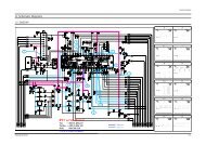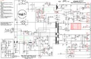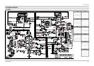
SERVICE MANUAL FOR M35&36; CHASSIS
SERVICE MANUAL FOR M35&36; CHASSIS
SERVICE MANUAL FOR M35&36; CHASSIS

Create successful ePaper yourself
Turn your PDF publications into a flip-book with our unique Google optimized e-Paper software.
TCL<br />
Chassis M35&<strong>36</strong> Service Manual<br />
terminated. The LW latch remains in the reset status.<br />
The LATCHED–OFF PHASE: The VCC capacitor voltage continues to drop. When it reaches 6.5V this<br />
phase is terminated. Its duration is governed by equation 3.<br />
The START–UP PHASE is reinitiated. The high voltage start–up current source (–ICC1 = 9mA) is activated<br />
and the MODE latch is reset. The VCC voltage ramps up according to the equation 1. When it reaches 13V,<br />
the IC enters into the SWITCHING PHASE.<br />
The NEXT SWITCHING PHASE: The high voltage current source is inhibited, the MODE latch (Q=0)<br />
activates the NORMAL mode of operation. Figure 2 shows that no current is injected out pin 2.<br />
The over current sense level corresponds to 1V.<br />
As long as the overload is present, this sequence repeats. The SWITCHING PHASE duty cycle is in the<br />
range of 10%.<br />
3. Transition from Normal to Pulsed Mode<br />
In this sequence the secondary side is reconfigured (refer to the typical application schematic). The high<br />
voltage output value becomes lower than the NORMAL mode regulated value. The TL431 shunt regulator<br />
is fully OFF. In the SMPS stand–by mode all the SMPS outputs are lowered except for the low voltage<br />
output that supply the wake–up circuit located at the isolated side of the power supply. In that mode the<br />
secondary regulation is performed by the zener diode connected in parallel to the TL431.<br />
The secondary reconfiguration status can be detected on the SMPS primary side by measuring the voltage<br />
level present on the auxiliary winding Laux. (Refer to the Demagnetization Section). In the reconfigured<br />
status, the Laux voltage is also reduced. The VCC self–powering is no longer possible thus the SMPS<br />
enters in a hiccup mode similar to the one described under the Overload condition.<br />
In the SMPS stand–by mode the 3 distinct phases are:<br />
The SWITCHING PHASE: Similar to the Overload mode. The current sense clamping level is reduced<br />
according to the equation of the current sense section. The C.S. clamping level depends on the power to<br />
be delivered to the load during the SMPS stand–by mode. Every switching sequence ON/OFF is<br />
terminated by an OC as long as the secondary Zener diode voltage has not been reached. When the<br />
Zener voltage is reached the ON cycle is terminated by a true PWM action. The proper SWITCHING<br />
PHASE termination must correspond to a NOC condition. The LW latch stores this NOC status.<br />
The LATCHED OFF PHASE: The MODE latch is set.<br />
The START–UP PHASE is similar to the Overload Mode. The MODE latch remains in its set status (Q=1).<br />
The SWITCHING PHASE: The Stand–by signal is validated and the 200 A is sourced out of the Current<br />
Sense pin 2.<br />
4. Transition from Stand–by to Normal<br />
The secondary reconfiguration is removed. The regulation on the low voltage secondary rail can no longer<br />
be achieved, thus at the end of the SWITCHING PHASE, no PWM condition can be encountered. The LW<br />
latch is reset.<br />
At the next WORKING PHASE a NORMAL mode status takes place.<br />
In order to become independent of the recovery time SWITCHING PHASE constant on the secondary side<br />
of the SMPS an additional reset input R2 is provided on the MODE latch. The condition Idemag