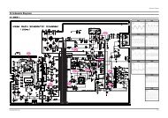
SERVICE MANUAL FOR M35&36; CHASSIS
SERVICE MANUAL FOR M35&36; CHASSIS
SERVICE MANUAL FOR M35&36; CHASSIS

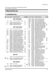
Create successful ePaper yourself
Turn your PDF publications into a flip-book with our unique Google optimized e-Paper software.
TCL<br />
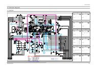
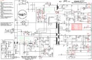
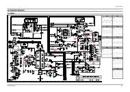
Chassis M35&<strong>36</strong> Service Manual<br />
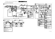
No. Pin Name Pin No. Type<br />
Connection<br />
(if not used)<br />
Short Description<br />
51 AIN1 51 IN GND S Analog Audio 1 Input<br />
52 AOUT2 52 OUT LV Analog Audio 2 Input<br />
53 AOUT1 1 53 OUT LV Analog Audio 2 Input<br />
54 VSUP S 54 SUPPLY X Supply Voltage, Standby<br />
55 GND S 55 SUPPLY X Ground, Standby<br />
56 XTAL1 56 IN X Analog Crystal Input<br />
57 XTAL2 57 OUT X Analog Crystal Output<br />
58 RESQ 58 IN/OUT X Reset Input/Output, Active Low<br />
59 SCL 59 IN/OUT X I 2 C Bus Clock<br />
60 SDA 60 IN/OUT X I 2 C Bus Data<br />
61 P23 61 IN/OUT LV Port2, Bit 3<br />
62 P22 62 IN/OUT LV Port2, Bit 2<br />
63 P21 63 IN/OUT LV Port2, Bit 1<br />
64 P20 64 IN/OUT LV Port2, Bit 0<br />
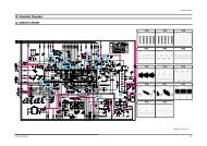
Pin Descriptions<br />
Pin 1,2,5-10, P10.P17 . I/O Port (Fig.1)<br />
These pins provide CPU controlled I/O ports.<br />
voltage. No supply current for the digital stages<br />
should flow through this line.<br />
Pin 3, VSUPP1* . Supply Voltage, Port 1 Driver<br />
This pin is used as supply for the I/O port 1 driver.<br />
Pin 4, GNDP1* . Ground, Port 1 Driver<br />
This is the ground reference for the I/O port 1 driver.<br />
Pin 11, VOUT. Analog Video Output (Fig. 2)<br />
The analog video signal that is selected for the main<br />
(luma, CVBS) adc is output at this pin. An emitter<br />
follower is required at this pin.<br />
Pin 12, VRT . Reference Voltage Top (Fig.3)<br />
Via this pin, the reference voltage for the A/D<br />
converters is decoupled. The pin is connected with<br />
10 ⎧F/47 nF to the Signal Ground Pin.<br />
Pin 13, SGND . Signal GND for Analog Input<br />
This is the high quality ground reference for the<br />
video input signals.<br />
Pin 14, GNDAF* . Ground, Analog Front-end<br />
This pin has to be connected to the analog ground.<br />
No supply current for the digital stages should flow<br />
through this line.<br />
Pin 16,18, CBINCRIN . Analog Chroma Component<br />
Input (Fig. 5)<br />
These pins are used as the chroma component (CB,<br />
CR) inputs required for the analog YUV Interface.<br />
The input signal must be AC-coupled. The CRIN pin<br />
can alternatively be used as the second SVHS<br />
chroma input (CIN2).<br />
Pin 17,18, CIN1CIN2 . Analog Chroma Input (Fig.<br />
4)<br />
These are the analog chroma inputs. A S-VHS<br />
chroma signal is converted using the chroma (Video<br />
2) AD converter. A resistive divider is used to bias<br />
the input signal to the middle of the converter input<br />
range. The input signal must be AC-coupled. The<br />
CIN2 pin can alternatively be used as the chroma<br />
component (CR) input required for the analog YUV<br />
Interface.<br />
Pins 19.22, VIN1–4 . Analog Video Input (Fig. 6)<br />
These are the analog video inputs. A CVBS or<br />
S-VHS luma signal is converted using the luma<br />
(Video 1) AD converter. The input signal must be<br />
AC-coupled.<br />
Pin 15, VSUPAF* . Supply Voltage, Analog Front-end<br />
This pin has to be connected to the analog supply<br />
Pin 23, TEST . Test Input (Fig. 7)<br />
This pin enables factory test modes. For normal<br />
42 03.Mar.2003