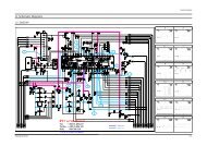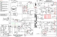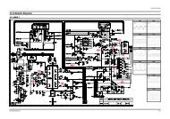
SERVICE MANUAL FOR M35&36; CHASSIS
SERVICE MANUAL FOR M35&36; CHASSIS
SERVICE MANUAL FOR M35&36; CHASSIS

You also want an ePaper? Increase the reach of your titles
YUMPU automatically turns print PDFs into web optimized ePapers that Google loves.
TCL<br />
Pins <strong>36</strong>, AGNDC – Internal Analog Reference Voltage<br />
This pin serves as the internal ground connection for<br />
the analog circuitry (except IF input). It must be connected<br />
to the VREF pins with a 3.3 ⎧F and a 100 nF<br />
capacitor in parallel. This pins shows a DC level of typically<br />
3.73 V.<br />
Pin 37, 38, NC – Pins not connected.<br />
Pins 39, 40, SC2_IN_L/R – SCART2 Inputs<br />
(Fig. 4)<br />
The analog input signal for SCART2 is fed to this pin.<br />
Analog input connection must be AC coupled.<br />
Pins 41, 42, SC1_IN_L/R – SCART1 Inputs<br />
(Fig. 4)<br />
The analog input signal for SCART1 is fed to this pin.<br />
Analog input connection must be AC coupled.<br />
Pin 43, VREFTOP – Reference Voltage IF AD Converter<br />
(Fig. 5)<br />
Via this pin, the reference voltage for the IF AD converter<br />
is decoupled. It must be connected to AVSS<br />
pins with a 10∀F and a 100nF capacitor in parallel.<br />
Traces must be kept short.<br />
Pin 44, MONO_IN – Mono Input (Fig. 4)<br />
The analog mono input signal is fed to this pin. Analog<br />
input connection must be AC coupled.<br />
Pins 45, AVSS* – Ground for Analog Power Supply<br />
Voltage<br />
Ground connection for the analog IF input circuitry of<br />
the MSP.<br />
Pins 46, AVSUP* – Analog Power Supply Voltage P-<br />
ower is supplied via this pin for the analog IF input<br />
circuitry of the MSP. This pin must be connected to the<br />
+5 V supply.<br />
Pin 47, ANA_IN1+ – IF Input 1 (Fig. 5)<br />
The analog sound if signal is supplied to this pin.<br />
Inputs must be AC coupled. This pin is designed as<br />
symmetrical input: ANA_IN1+ is internally connected<br />
to one input of a symmetrical op amp, ANA_IN. to the<br />
other.<br />
Chassis M35&<strong>36</strong> Service Manual<br />
Pin 48, ANA_IN. – IF Common (Fig. 5)<br />
This pin serves as a common reference for ANA_<br />
IN1/2+ inputs.<br />
Pin 49, NC – Pin not connected<br />
Pin 50, TESTEN – Test Enable Pin (Fig. 2)<br />
This pin enables factory test modes. For normal<br />
operation it must be connected to ground.<br />
Pins51, 52, XTAL_INXTAL_OUT – Crystal Input<br />
and Output Pins (Fig. 10)<br />
These pins are connected to an 18.432 MHz crystal<br />
oscillator which is digitally tuned by integrated<br />
shunt capacitances. An external clock can be fed<br />
into XTAL_IN. The audio clock output signal AUD_<br />
CL_OUT is derived form the oscillator. External capacitors<br />
at each crystal pin to ground (AVSS) are<br />
required. It should be verified by layout, that no<br />
supply current for the digital circuitry is flowing<br />
through the ground connection point.<br />
* Application Note:<br />
All ground pins should be connected to one low-<br />
Resistive ground plane. All supply pins should be<br />
connected separately with short and low-resistive<br />
lines to the power supply. Decoupling capacitors<br />
from DVSUP to DVSS, AVSUP to AVSS, and AH-<br />
VSUP to AHVSS are recommended as closely as<br />
possible to these pins. Decoupling of DVSUP and<br />
DVSS is most important. We recommend using<br />
more than one capacitor. By choosing different<br />
values, the frequency range of active decoupling<br />
can be extended. In our application boards we use:<br />
220 pF, 470 pF, 1.5 nF, and 10 ⎧F. The capacitor<br />
with the lowest value should be placed nearest to<br />
the DVSUP and DVSS pins.<br />
34 03.Mar.2003