Manufacturing and Reliability Challenges With QFN - American ...
Manufacturing and Reliability Challenges With QFN - American ...
Manufacturing and Reliability Challenges With QFN - American ...

Create successful ePaper yourself
Turn your PDF publications into a flip-book with our unique Google optimized e-Paper software.
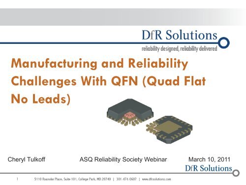
<strong>Manufacturing</strong> <strong>and</strong> <strong>Reliability</strong><br />
<strong>Challenges</strong> <strong>With</strong> <strong>QFN</strong> (Quad Flat<br />
No Leads)<br />
Cheryl Tulkoff<br />
ASQ <strong>Reliability</strong> Society Webinar March 10, 2011<br />
1
Instructor Biography<br />
o<br />
o<br />
o<br />
Cheryl Tulkoff has over 17 years of experience in electronics manufacturing<br />
with an emphasis on failure analysis <strong>and</strong> reliability. She has worked throughout<br />
the electronics manufacturing life cycle beginning with semiconductor fabrication<br />
processes, into printed circuit board fabrication <strong>and</strong> assembly, through<br />
functional <strong>and</strong> reliability testing, <strong>and</strong> culminating in the analysis <strong>and</strong> evaluation<br />
of field returns. She has also managed no clean <strong>and</strong> RoHS-compliant conversion<br />
programs <strong>and</strong> has developed <strong>and</strong> managed comprehensive reliability<br />
programs.<br />
Cheryl earned her Bachelor of Mechanical Engineering degree from Georgia<br />
Tech. She is a published author, experienced public speaker <strong>and</strong> trainer <strong>and</strong> a<br />
Senior member of both ASQ <strong>and</strong> IEEE. She holds leadership positions in the IEEE<br />
Central Texas Chapter, IEEE WIE (Women In Engineering), <strong>and</strong> IEEE ASTR<br />
(Accelerated Stress Testing <strong>and</strong> <strong>Reliability</strong>) sections. She chaired the annual IEEE<br />
ASTR workshop for four years <strong>and</strong> is also an ASQ Certified <strong>Reliability</strong><br />
Engineer.<br />
She has a strong passion for pre-college STEM (Science, Technology,<br />
Engineering, <strong>and</strong> Math) outreach <strong>and</strong> volunteers with several organizations that<br />
specialize in encouraging pre-college students to pursue careers in these fields.<br />
2
DfR Solutions works with companies <strong>and</strong> individuals throughout the life cycle<br />
of a product, lending a guiding h<strong>and</strong> on quality, reliability <strong>and</strong> durability<br />
(QRD) issues that allows your staff to focus on creativity <strong>and</strong> ideas.<br />
Our expertise in the emerging science of Electrical <strong>and</strong> Electronics <strong>Reliability</strong><br />
Physics provides crucial insights <strong>and</strong> solutions early in product design,<br />
development <strong>and</strong> test throughout manufacturing, <strong>and</strong> even into the field.<br />
3
Who is DfR Solutions?<br />
o<br />
We use Physics-of-Failure<br />
(PoF) <strong>and</strong> Best Practices<br />
expertise to provide knowledgebased<br />
strategic quality <strong>and</strong><br />
reliability solutions to the<br />
electronics industry<br />
o<br />
o<br />
o<br />
o<br />
o<br />
Technology Insertion<br />
Design<br />
<strong>Manufacturing</strong> <strong>and</strong> Supplier Selection<br />
Product Validation <strong>and</strong> Accelerated Testing<br />
Root-Cause Failure Analysis & Forensics Engineering<br />
o<br />
Unique combination of expert consultants <strong>and</strong> state-of-the-art laboratory<br />
facilities<br />
4
DfR Clients<br />
o<br />
o<br />
o<br />
o<br />
o<br />
o<br />
o<br />
o<br />
o<br />
o<br />
o<br />
o<br />
o<br />
o<br />
o<br />
o<br />
o<br />
o<br />
o<br />
o<br />
o<br />
o<br />
o<br />
o<br />
o<br />
o<br />
o<br />
o<br />
o<br />
o<br />
o<br />
o<br />
o<br />
o<br />
o<br />
o<br />
Military / Avionics / Space<br />
Rockwell Collins<br />
DRS<br />
Honeywell<br />
Applied Data Systems<br />
Mercury Computers<br />
Digital Receiver Technology<br />
Hamilton Sundstr<strong>and</strong><br />
Kato Engineering<br />
Thales Communications<br />
L-3 Communications<br />
Innovative Concepts<br />
S<strong>and</strong>ia National Labs<br />
Crane (Eldec)<br />
ViaSat<br />
Eaton<br />
Automotive / Commercial Vehicle<br />
General Motors<br />
Caterpillar<br />
Panasonic Automotive<br />
Hella Automotive<br />
LG Electronics<br />
Tyco Electronics<br />
TRW<br />
MicroHeat<br />
Medical<br />
Biotronik<br />
Philips Medical<br />
Abbott Laboratories<br />
Tecan Systems<br />
Neuropace<br />
Inter-Metro<br />
Welch Allyn<br />
Guidant / Boston Scientific<br />
Beckman Coulter<br />
Applied Biosystems<br />
Cardinal Health<br />
Medtronic<br />
Cardiac Science<br />
o<br />
o<br />
o<br />
o<br />
o<br />
o<br />
o<br />
o<br />
o<br />
o<br />
o<br />
o<br />
o<br />
o<br />
o<br />
o<br />
o<br />
o<br />
o<br />
o<br />
o<br />
o<br />
o<br />
o<br />
o<br />
o<br />
o<br />
o<br />
o<br />
o<br />
o<br />
o<br />
o<br />
o<br />
o<br />
o<br />
Server / Telecom<br />
Lucent Technologies<br />
Sun Microsystems<br />
Cisco Systems<br />
Artesyn Communications<br />
Corvis Communications<br />
Huawei (China)<br />
Airgo Networks<br />
Verigy<br />
Antares ATT<br />
Enterasys<br />
True Position<br />
HiFN<br />
Cedar Point<br />
Optics1<br />
Tropos Networks<br />
Consumer / Appliance<br />
Fujitsu (Japan)<br />
Dell Computers<br />
Samsung (Korea)<br />
LG Electronics (Korea)<br />
Tubitak Mam (Turkey)<br />
Insinkerator<br />
White Rodgers<br />
Emerson Appliance Controls<br />
Therm-O-Disc<br />
NMB Technologies<br />
Shure<br />
H<strong>and</strong>i-Quilt<br />
Xerox<br />
Portables<br />
RSA Security<br />
H<strong>and</strong>held<br />
Kyocera<br />
LG Electronics<br />
Contract Manufacturers<br />
Daeduck (Korea)<br />
Gold Circuit Electronics (Taiwan)<br />
Engent<br />
EIT<br />
Industrial / Power<br />
• Schlumberger<br />
• Copel<strong>and</strong><br />
• Tennant<br />
• Rosemount<br />
• Branson<br />
• Computer Process Controls<br />
• ASCO Power<br />
• ASCO Valve<br />
• Astec<br />
• Liebert<br />
• Avansys<br />
• Tyco Electronics<br />
• Rainbird<br />
• MicroMotion<br />
• Siemens<br />
• Barco<br />
• Calex<br />
• Western Geco (Norway)<br />
• General Electric<br />
• Ingersoll R<strong>and</strong><br />
• Fusion UV<br />
• Numatics<br />
• Durotech<br />
• Danaher Motion<br />
• TallyGencom<br />
• Vision Research<br />
• Olympus NDT<br />
Components<br />
• Fairchild Semiconductor<br />
• Maxtek<br />
• Samsung ElectroMechanics (Korea)<br />
• Pulse<br />
• Teradyne<br />
• Amphenol<br />
• AVX<br />
• Anadigics<br />
• Kemet<br />
• NIC<br />
• Graftech<br />
• International Rectifier<br />
5
Selected Publications<br />
o<br />
o<br />
o<br />
o<br />
o<br />
o<br />
o<br />
o<br />
o<br />
o<br />
o<br />
o<br />
o<br />
o<br />
o<br />
Epidemiological Study of SnAgCu Solder: Benchmarking Results from Accelerated Life Testing<br />
What I Don„t Know That I Don„t Know: Things to Worry About with the Pb-Free Transition<br />
Long-term <strong>Reliability</strong> of Pb-free Electronics<br />
Robustness of Ceramic Capacitors Assembled with Pb-Free Solder<br />
Failure Mechanisms in LED <strong>and</strong> Laser Diodes<br />
Microstructure <strong>and</strong> Damage Evolution in Pb-Free Solder Joints<br />
Improved Methodologies for Identifying Root-Cause of Printed Board Failures<br />
<strong>Reliability</strong> of Pressure Sensitive Adhesive Tapes for Heat Sink Attachment<br />
Failure Mechanisms in Electronic Products at High Altitudes<br />
Determining the Lifetime of Conductive Adhesive / Solder Plated Interconnections<br />
Issues in Long-Term Storage of Plastic Encapsulated Microcircuits<br />
Effect of PWB Plating on the Microstructure <strong>and</strong> <strong>Reliability</strong> of SnAgCu Solder Joints<br />
A Demonstration of Virtual Qualification for the Design of Electronic Hardware<br />
Solder Failure Mechanisms in Single-Sided Insertion-Mount Printed Wiring Boards<br />
Finite Element Modeling of Printed Circuit Boards for Structural Analysis<br />
6
DfR Resources <strong>and</strong> Equipment<br />
Electrical<br />
o Oscilloscopes<br />
o<br />
o<br />
o<br />
o<br />
o<br />
o<br />
o<br />
o<br />
Digital<br />
Analog<br />
Curve Tracers<br />
o<br />
o<br />
Digital<br />
Analog<br />
Partial Discharge Detector<br />
Capacitance Meters<br />
Low Resistance Meters<br />
High Resistance Meters<br />
High Voltage Power Supplies (Hi-Pot)<br />
Testing<br />
o HALT<br />
o Temperature Cycling<br />
o Thermal Shock<br />
o Temperature/Humidity<br />
o Vibration<br />
o Mechanical Shock / Drop Tower<br />
o Mixed Flowing Gas<br />
o Salt Spray<br />
o Capacitor Testing (Ripple Current)<br />
Material Analysis<br />
o X-ray<br />
o Acoustic Microscopy<br />
o Infrared Camera<br />
o Metallographic Preparation<br />
o Stereoscope<br />
o Optical Microscope<br />
o Scanning Electron Microscope<br />
o Energy Dispersive Spectroscopy<br />
o Ion Chromatography<br />
o FTIR (Solid / Film / Liquid)<br />
o Thermomechanical Analyzer<br />
o SQUID Microscopy<br />
o Xray Diffraction<br />
o Focused Ion Beam Imaging<br />
o XPS<br />
Other<br />
o Circuit Simulation<br />
o Finite Element Analysis (FEA)<br />
o Computational Fluid Dynamics<br />
o <strong>Reliability</strong> Prediction (Physics of Failure)<br />
7
Knowledge <strong>and</strong> Education (Website)<br />
o<br />
Let your staff learn<br />
all day / every day<br />
o<br />
o<br />
o<br />
o<br />
o<br />
E-LEARNING<br />
Scholarly articles<br />
Technical white papers<br />
Case studies<br />
<strong>Reliability</strong> calculators<br />
Online presentations<br />
8<br />
8
<strong>QFN</strong> as a ‘Next Generation’ Technology<br />
o<br />
o<br />
o<br />
What is „Next Generation‟ Technology?<br />
o<br />
Materials or designs currently<br />
being used, but not widely adopted<br />
(especially among hi-rel manufacturers)<br />
Carbon nanotubes are not<br />
„Next Generation‟<br />
o<br />
Not used in electronic applications<br />
Ball grid array is not<br />
„Next Generation‟<br />
o<br />
Widely adopted<br />
9<br />
9
Introduction (cont.)<br />
o<br />
o<br />
o<br />
Why is knowing about „Next<br />
Generation‟ Technologies important?<br />
These are the technologies that you<br />
or your supply chain will use to<br />
improve your product<br />
o<br />
Cheaper, Faster, Stronger,<br />
„Environmentally-Friendly‟, etc.<br />
And sooner then you think!<br />
10<br />
10
<strong>Reliability</strong> <strong>and</strong> Next Generation Technologies<br />
o<br />
o<br />
o<br />
One of the most common drivers for failure is<br />
inappropriate adoption of new technologies<br />
o<br />
The path from consumer (high volume, short lifetime) to high rel is<br />
not always clear<br />
Obtaining relevant information<br />
can be difficult<br />
o<br />
o<br />
Information is often segmented<br />
Focus on opportunity, not risks<br />
Can be especially true for<br />
component packaging<br />
o<br />
BGA (Ball Grid Array), flip chip, <strong>QFN</strong> (Quad Flat No Lead)<br />
11<br />
11
Component Packaging<br />
o<br />
Most of us have little influence over component packaging<br />
o<br />
Most devices offer only one or two packaging styles<br />
o<br />
Why should you care?<br />
o<br />
o<br />
Poor underst<strong>and</strong>ing of component qualification procedures<br />
Who tests what <strong>and</strong> why?<br />
12<br />
12
Component Testing<br />
o<br />
o<br />
o<br />
<strong>Reliability</strong> testing performed by component manufacturers<br />
is driven by JEDEC<br />
o JESD22 series (A & B)<br />
Focus is almost entirely on die, packaging, <strong>and</strong> 1 st level<br />
interconnections (wire bond, solder bump, etc.)<br />
Only focus on 2 nd level interconnects (solder joints) is<br />
JESD22-B113 Cyclic Bend Test<br />
o<br />
o<br />
Driven by cell phone industry<br />
They have little interest in thermal cycling or vibration!<br />
13<br />
13
2 nd Level Interconnect <strong>Reliability</strong><br />
o<br />
o<br />
o<br />
IPC has attempted to rectify this through<br />
IPC-9701<br />
Two problems<br />
o<br />
o<br />
Adopted by OEMs; not by component manufacturers<br />
Application specific; you have to tell them the application<br />
(your responsibility, not theirs)<br />
The result<br />
o<br />
An increasing incidence of solder wearout in next generation<br />
component packaging<br />
14<br />
14
Solder Wearout in Next Generation Packaging<br />
o<br />
o<br />
o<br />
Performance Needs<br />
Higher frequencies <strong>and</strong> data transfer rates<br />
o<br />
Lower resistance-capacitance (RC) constants<br />
Higher densities<br />
o<br />
More inside less plastic<br />
Lower voltage, but higher current<br />
o<br />
Joule heating is I 2 R<br />
o<br />
Has resulted in less robust package designs<br />
15<br />
15
Solder Wearout (cont.)<br />
o<br />
Elimination of leaded devices<br />
o<br />
o<br />
Provides lower resistance-capacitance (RC) <strong>and</strong> higher package<br />
densities<br />
Reduces compliance<br />
Cycles to failure<br />
-40 to 125C<br />
QFP: >10,000 BGA: 3,000 to 8,000<br />
CSP / Flip Chip:
Solder Wearout (cont.)<br />
o<br />
o<br />
Design change: More silicon, less plastic<br />
Increases mismatch in coefficient of thermal expansion<br />
(CTE)<br />
BOARD LEVEL ASSEMBLY AND RELIABILITY<br />
CONSIDERATIONS FOR <strong>QFN</strong> TYPE PACKAGES,<br />
Ahmer Syed <strong>and</strong> WonJoon Kang, Amkor Technology.<br />
17<br />
17
Characteristic Life (Cycles to Failure)<br />
Solder Wearout (cont.)<br />
o<br />
Hotter devices<br />
o<br />
Increases change in temperature (DT)<br />
10000<br />
t f = DT n<br />
9000<br />
8000<br />
7000<br />
n = 2 (SnPb)<br />
n = 2.3 (SnNiCu)<br />
n = 2.7 (SnAgCu)<br />
6000<br />
5000<br />
4000<br />
3000<br />
2000<br />
1000<br />
0<br />
0 50 100 150 200<br />
Change in Temperature ( o C)<br />
18<br />
18
Industry Response to SJ Wearout?<br />
o<br />
o<br />
JEDEC<br />
o<br />
Specification body for component manufacturers<br />
JEDEC JESD47<br />
o<br />
o<br />
o<br />
Guidelines for new component qualification<br />
Requires 2300 cycles of 0 to 100C<br />
Testing is often done on thin boards<br />
o<br />
IPC<br />
o<br />
o IPC 9701<br />
o<br />
o<br />
Specification body for electronic OEMs<br />
Recommends 6000 cycles of 0 to 100C<br />
Test boards should be similar thickness as<br />
actual design<br />
19<br />
19
BIG PROBLEM<br />
o<br />
o<br />
JEDEC requirements are 60% less than IPC<br />
Testing on a thin board can extend lifetimes by 2X to 4X<br />
o<br />
What does this mean?<br />
o<br />
The components you buy may only survive<br />
500 cycles of 0 to 100C<br />
o<br />
What must you do?<br />
o<br />
Components at risk must be subjected to PoF-based (Physics of<br />
Failure) reliability analysis<br />
20<br />
20
Quad Flat Pack No Leads or<br />
Quad Flat No Leads<br />
(<strong>QFN</strong>)<br />
21<br />
21
<strong>QFN</strong>: What is it?<br />
o<br />
o<br />
Quad Flat Pack No Lead or Quad Flat Non-Leaded<br />
o „The poor man‟s ball grid array‟<br />
o Also known as<br />
o<br />
o<br />
o<br />
Leadframe Chip Scale Package (LF-CSP)<br />
MicroLeadFrame (MLF)<br />
Others (MLP, LPCC, QLP, HV<strong>QFN</strong>, etc.)<br />
Overmolded leadframe with bond pads exposed on the bottom <strong>and</strong><br />
arranged along<br />
the periphery of the package<br />
o Developed in the early to<br />
mid-1990‟s by Motorola,<br />
Toshiba, Amkor, etc.<br />
o St<strong>and</strong>ardized by JEDEC/EIAJ in<br />
late-1990‟s<br />
o Fastest growing package type<br />
22<br />
22
<strong>QFN</strong> Advantages: Size <strong>and</strong> Cost<br />
o<br />
o<br />
Smaller, lighter <strong>and</strong> thinner than comparable leaded<br />
packages<br />
o<br />
Allows for greater functionality per volume<br />
Reduces cost<br />
o<br />
o<br />
Component manufacturers: More ICs per frame<br />
OEMs: Reduced board size<br />
o<br />
Attempts to limit the footprint of lower I/O devices have<br />
previously been stymied for cost reasons<br />
o<br />
BGA materials <strong>and</strong> process too expensive<br />
23<br />
23
Advantages: Manufacturability<br />
o<br />
o<br />
Small package without placement <strong>and</strong> solder printing<br />
constraints of fine pitch leaded devices<br />
o<br />
o<br />
o<br />
o<br />
No special h<strong>and</strong>ling/trays to avoid bent or non planar pins<br />
Easier to place correctly on PCB pads than fine pitch QFPs,<br />
TSOPs, etc.<br />
Larger pad geometry makes for simpler solder paste printing<br />
Less prone to bridging defects when proper pad design <strong>and</strong><br />
stencil apertures are used.<br />
Reduced popcorning moisture sensitivity issues – smaller<br />
package<br />
24<br />
24
Advantages: Thermal Performance<br />
o<br />
o<br />
More direct thermal path with larger area<br />
o<br />
Die Die Attach Thermal Pad <br />
Solder Board Bond Pad<br />
qJa for the <strong>QFN</strong> is about half of a<br />
leaded counterpart (as per JESD-51)<br />
o<br />
Allows for 2X increase in power dissipation<br />
25<br />
25
Advantages: Inductance<br />
o<br />
o<br />
At higher operating frequencies, inductance of the gold<br />
wire <strong>and</strong> long lead-frame traces will affect performance<br />
Inductance of <strong>QFN</strong> is half its leaded counterpart because<br />
it eliminates gullwing leads <strong>and</strong> shortens wire lengths<br />
Popular for<br />
RF Designs<br />
http://ap.pennnet.com/display_article/153955/36/ARTCL/none/none/1/The-back-end-process:-Step-9-<strong>QFN</strong>-Singulation/<br />
26<br />
26
<strong>QFN</strong>: Why Not?<br />
o<br />
o<br />
<strong>QFN</strong> is a „next generation‟ technology for non-consumer<br />
electronic OEMs due to concerns with<br />
o<br />
o<br />
o<br />
Manufacturability<br />
Compatibility with other OEM processes<br />
<strong>Reliability</strong><br />
Acceptance of this package, especially in long-life, severe<br />
environment, high-rel applications, is currently limited as a<br />
result<br />
27<br />
27
<strong>QFN</strong> Manufacturability: Bond Pads<br />
o<br />
o<br />
o<br />
Non Solder Mask Defined Pads Preferred (NSMD)<br />
o<br />
o<br />
Copper etch process has tighter process control than solder mask process<br />
Makes for more consistent, strong solder joints since solder bonds to both tops <strong>and</strong> sides of pads<br />
Use solder mask defined pads (SMD) with care<br />
o<br />
o<br />
Can be used to avoid bridging between pads, especially between thermal <strong>and</strong> signal pads.<br />
Pads can grow in size quite a bit based on PCB mfg capabilities<br />
Can lose solder volume <strong>and</strong> st<strong>and</strong>off height through vias in thermal pads<br />
o<br />
o<br />
o<br />
o<br />
o<br />
o<br />
o<br />
May need to tent, plug, or cap vias to keep sufficient paste volume<br />
Reduced st<strong>and</strong>off weight reduces cleanability <strong>and</strong> pathways for flux outgassing<br />
o Increased potential for contamination related failures<br />
Tenting <strong>and</strong> plugging vias is often not well controlled <strong>and</strong> can lead to placement <strong>and</strong> chemical<br />
entrapment issues<br />
Exercise care with devices placed on opposing side of <strong>QFN</strong><br />
Can create placement issues if solder “bumps” are created in vias<br />
Can create solder short conditions on the opposing device<br />
Capping is a more robust, more expensive process that eliminates these concerns<br />
28<br />
28
o<br />
Increase component st<strong>and</strong>off through PCB design<br />
One option: Soldermask Lift<br />
29
Bond Pads (cont.)<br />
o<br />
Extend bond pad 0.2 – 0.3 mm beyond<br />
package footprint<br />
o<br />
o<br />
May or may not solder to cut edge<br />
Allows for better visual inspection<br />
o<br />
Really need X-ray for best results<br />
o<br />
o<br />
Allows for verification of bridging,<br />
adequate solder coverage <strong>and</strong><br />
void percentage<br />
Note: Lacking in good criteria<br />
for acceptable voiding<br />
30<br />
30
Manufacturability: Stencil Design<br />
o<br />
o<br />
o<br />
Stencil thickness <strong>and</strong> aperture design can be crucial for<br />
manufacturability<br />
o Excessive amount of paste can induce<br />
float, lifting the <strong>QFN</strong> off the board<br />
o Excessive voiding can also be induced<br />
through inappropriate stencil design<br />
Follow manufacturer‟s guidelines<br />
o Goal is 2-3 mils of solder thickness<br />
Rules of thumb (thermal pad)<br />
o Ratio of aperture/pad ~0.5:1<br />
o Consider multiple, smaller apertures<br />
(avoid large bricks of solder paste)<br />
o Reduces propensity for solder balling<br />
31<br />
31
Manufacturability: Stencil Design<br />
Datasheet says solder paste coverage should be 40-80%<br />
Drawing supplied in same datasheet is for 26% coverage<br />
32<br />
32
Manufacturability: Reflow & Moisture<br />
o<br />
o<br />
o<br />
o<br />
<strong>QFN</strong> solder joints are more susceptible to dimensional changes<br />
Case Study: Military supplier experienced solder separation under <strong>QFN</strong><br />
<strong>QFN</strong> supplier admitted that the package was more susceptible to moisture<br />
absorption that initially expected<br />
o Resulted in transient swelling during reflow soldering<br />
o Induced vertical lift, causing solder separation<br />
Was not popcorning<br />
o No evidence of cracking or delamination in component package<br />
33<br />
33
Corrective Actions: <strong>Manufacturing</strong><br />
Verify good MSL h<strong>and</strong>ling/procedures<br />
Spec <strong>and</strong> confirm - Reflow<br />
Room temperature to preheat (max 2-3 o C/sec)<br />
Preheat to at least 150 o C<br />
Preheat to maximum temperature (max 4-5 o C/sec)<br />
Cooling (max 2-3 o C/sec)<br />
In conflict with profile from J-STD-020C (6 o C/sec)<br />
Make sure assembly is less than 60 o C before cleaning<br />
34<br />
34
Manufacturability: <strong>QFN</strong> Joint Inspection<br />
35<br />
35
Manufacturability: <strong>QFN</strong> Joint Inspection<br />
36<br />
36
Manufacturability: <strong>QFN</strong> Joint Inspection<br />
Convex or absence of fillet highly likely<br />
•Etching of leadframe can prevent<br />
pad from reaching edge of package<br />
•Edge of bond pad is not plated for<br />
solderability<br />
37<br />
37
Manufacturability: <strong>QFN</strong> Joint Inspection<br />
o<br />
A large convex fillet is often an indication of issues<br />
o<br />
o<br />
o<br />
Poor wetting under the <strong>QFN</strong><br />
Tilting due to excessive solder paste under the thermal pad<br />
Elevated solder surface tension, from insufficient solder paste<br />
under the thermal pad, pulling the package down<br />
38<br />
38
Manufacturability: Rework<br />
o<br />
o<br />
o<br />
Can be difficult to replace a package <strong>and</strong> get adequate<br />
soldering of thermal / internal pads.<br />
o<br />
Mini-stencils, preforms, or rebump techniques can be used to get<br />
sufficient solder volume<br />
Not directly accessible with soldering iron <strong>and</strong> wire<br />
o<br />
Portable preheaters used in conjunction with soldering iron can<br />
simplify small scale repair processes<br />
Close proximity with capacitors often requires adjacent<br />
components to be resoldered / replaced as well<br />
39<br />
39
Manufacturability: Board Flexure<br />
o<br />
Area array devices are known to have board flexure<br />
limitations<br />
o<br />
For SAC attachment, maximum microstrain can be as low as<br />
500 ue<br />
o<br />
<strong>QFN</strong> has an even lower level of compliance<br />
o<br />
o<br />
o<br />
Limited quantifiable knowledge in this area<br />
Must be conservative during board build<br />
IPC is working on a specification similar to BGAs<br />
40<br />
40
Pad Cratering<br />
• Cracking initiating within the laminate during a dynamic mechanical event<br />
<br />
In circuit testing (ICT), board depanelization, connector insertion, shock <strong>and</strong><br />
vibration, etc.<br />
G. Shade, Intel (2006)<br />
41<br />
41<br />
41
Pad Cratering<br />
Intel (2006)<br />
o<br />
Drivers<br />
o<br />
o<br />
o<br />
o<br />
Finer pitch components<br />
More brittle laminates<br />
Stiffer solders (SAC vs. SnPb)<br />
Presence of a large heat sink<br />
o<br />
Difficult to detect using<br />
st<strong>and</strong>ard procedures<br />
o<br />
X-ray, dye-n-pry, ball shear, <strong>and</strong><br />
ball pull<br />
42<br />
42<br />
42
Solutions to Pad Cratering<br />
o<br />
Board Redesign<br />
o<br />
Solder mask defined vs. non-solder mask defined<br />
o<br />
o<br />
o<br />
o<br />
Limitations on board flexure<br />
o<br />
750 to 500 microstrain, Component dependent<br />
More compliant solder<br />
o<br />
SAC305 is relatively rigid, SAC105 <strong>and</strong> SNC are possible<br />
alternatives<br />
New acceptance criteria for laminate materials<br />
o<br />
o<br />
Intel-led industry effort<br />
Attempting to characterize laminate material using high-speed<br />
ball pull <strong>and</strong> shear testing, Results inconclusive to-date<br />
Alternative approach<br />
o<br />
Require reporting of fracture toughness <strong>and</strong> elastic modulus<br />
43<br />
43<br />
43
<strong>Reliability</strong>: Thermal Cycling<br />
o<br />
Order of magnitude reduction in time to<br />
failure from QFP<br />
o<br />
3X reduction from BGA<br />
QFP: >10,000<br />
o<br />
Driven by die / package ratio<br />
o 40% die; tf = 8K cycles (-40 / 125C)<br />
o 75% die; tf = 800 cycles (-40 / 125C)<br />
o<br />
Driven by size <strong>and</strong> I/O#<br />
o 44 I/O; tf = 1500 cycles (-40 / 125C)<br />
o 56 I/O; tf = 1000 cycles (-40 / 125C)<br />
BGA: 3,000 to 8,000<br />
o<br />
Very dependent upon solder bond with<br />
thermal pad<br />
<strong>QFN</strong>: 1,000 to 3,000<br />
44<br />
44
Thermal Cycling: Conformal Coating<br />
o<br />
Care must be taken when using conformal coating over <strong>QFN</strong><br />
o<br />
o<br />
Coating can infiltrate under the <strong>QFN</strong><br />
Small st<strong>and</strong>off height allows coating to cause lift<br />
o Hamilton Sundstr<strong>and</strong> found a significant reduction in time to failure (-<br />
55 / 125C)<br />
o<br />
o<br />
o<br />
Uncoated: 2000 to 2500 cycles<br />
Coated: 300 to 700 cycles<br />
Also driven by solder joint<br />
sensitivity to tensile stresses<br />
o<br />
Damage evolution is far<br />
higher than for shear stresses<br />
Wrightson, SMTA Pan Pac 2007<br />
45<br />
45
<strong>Reliability</strong>: Bend Cycling<br />
o<br />
Low degree of compliance<br />
<strong>and</strong> large footprint can<br />
also result in issues during<br />
cyclic flexure events<br />
o<br />
Example: IR tested a<br />
5 x 6mm <strong>QFN</strong> to<br />
JEDEC JESD22-B113<br />
o Very low beta (~1)<br />
o<br />
Suggests brittle fracture, possible along the interface<br />
46<br />
46
<strong>Reliability</strong>: Dendritic Growth / Electrochemical Migration<br />
o<br />
o<br />
o<br />
Large area, multi-I/O <strong>and</strong> low st<strong>and</strong>off can trap flux<br />
under the <strong>QFN</strong><br />
Processes using no-clean flux should be requalified<br />
o<br />
Particular configuration could result in weak organic acid<br />
concentrations above maximum (150 – 200 ug/in 2 )<br />
Those processes not using no-clean flux will likely<br />
experience dendritic growth without modification of<br />
cleaning process<br />
o<br />
o<br />
o<br />
Changes in water temperature<br />
Changes in saponifier<br />
Changes to impingement jets<br />
47<br />
47
Dendritic Growth (cont.)<br />
o<br />
o<br />
o<br />
o<br />
The electric field strength between adjacent conductors is a strong<br />
driver for dendritic growth<br />
o Voltage / distance<br />
Digital technology typically has a maximum field strength of<br />
0.5 V/mil<br />
o TSSOP80 with 3.3VDC power <strong>and</strong> 16 mil pitch<br />
Previous generation analog / power technology had a maximum field<br />
strength of 1.6 V/mil<br />
o SOT23 with 50VDC power <strong>and</strong> 50 mil pitch<br />
Introduction of <strong>QFN</strong> has resulted in electric fields as high as<br />
3.5 V/mil<br />
o 24VDC <strong>and</strong> 16 mil pitch<br />
48<br />
48
Dendritic Growth (cont.)<br />
o<br />
Component manufacturers are increasingly aware of this<br />
issue <strong>and</strong> separate power <strong>and</strong> ground<br />
o<br />
o<br />
Linear Technologies (left) has strong separation power <strong>and</strong><br />
ground<br />
Intersil (right) has power <strong>and</strong> ground on adjacent pins<br />
49<br />
49
Electro-Chemical Migration: Details<br />
o<br />
Insidious failure mechanism<br />
o Self-healing: leads to large number<br />
of no-trouble-found (NTF)<br />
o Can occur at nominal voltages (5 V)<br />
<strong>and</strong> room conditions (25C, 60%RH)<br />
elapsed time<br />
12 sec.<br />
o<br />
o<br />
Due to the presence of contaminants<br />
on the surface of the board<br />
o Strongest drivers are halides (chlorides <strong>and</strong> bromides)<br />
o Weak organic acids (WOAs) <strong>and</strong> polyglycols can also lead to drops in the<br />
surface insulation resistance<br />
Primarily controlled through controls on cleanliness<br />
o Minimal differentiation between existing Pb-free solders, SAC <strong>and</strong> SnCu,<br />
<strong>and</strong> SnPb<br />
o Other Pb-free alloys may be more susceptible (e.g., SnZn)<br />
50<br />
50<br />
50
Cleanliness Recommendations<br />
Ion Control Maximum<br />
Fluoride N/A 1 mg/in 2<br />
Chloride 2 mg/in 2 4.5 mg/in 2<br />
Bromide 10 mg/in 2 15 mg/in 2<br />
Nitrates, Sulfates 2 – 4 mg/in 2 6 – 12 mg/in 2<br />
WOAs 150 mg/in 2 250 mg/in 2<br />
51<br />
51
<strong>QFN</strong>: Risk Mitigation<br />
o<br />
o<br />
Assess manufacturability<br />
o<br />
o<br />
o<br />
o<br />
o<br />
DOE on stencil design<br />
Degree of reflow profiling<br />
Control of board flexure<br />
Dual row <strong>QFN</strong> is especially difficult<br />
Cleanliness is critical<br />
Assess reliability<br />
o<br />
o<br />
o<br />
Ownership of 2 nd level interconnect<br />
is often lacking<br />
Extrapolate to needed field reliability<br />
Some companies have reballed <strong>QFN</strong><br />
to deal with concerns<br />
52<br />
52
Thank you!<br />
Any Questions?<br />
Contact me:<br />
ctulkoff@dfrsolutions.com<br />
www.dfrsolutions.com<br />
53
Disclaimer & Confidentiality<br />
o<br />
o<br />
o<br />
ANALYSIS INFORMATION<br />
This report may include results obtained through analysis performed by DfR Solutions‟<br />
Sherlock software. This comprehensive tool is capable of identifying design flaws <strong>and</strong><br />
predicting product performance. For more information, please contact<br />
DfRSales@dfrsolutions.com.<br />
DISCLAIMER<br />
DfR represents that a reasonable effort has been made to ensure the accuracy <strong>and</strong><br />
reliability of the information within this report. However, DfR Solutions makes no<br />
warranty, both express <strong>and</strong> implied, concerning the content of this report, including, but<br />
not limited to the existence of any latent or patent defects, merchantability, <strong>and</strong>/or<br />
fitness for a particular use. DfR will not be liable for loss of use, revenue, profit, or any<br />
special, incidental, or consequential damages arising out of, connected with, or<br />
resulting from, the information presented within this report.<br />
CONFIDENTIALITY<br />
The information contained in this document is considered to be proprietary to DfR<br />
Solutions <strong>and</strong> the appropriate recipient. Dissemination of this information, in whole or<br />
in part, without the prior written authorization of DfR Solutions, is strictly prohibited.<br />
From all of us at DfR Solutions, we would like to thank you for choosing us as your<br />
partner in quality <strong>and</strong> reliability assurance. We encourage you to visit our website for<br />
information on a wide variety of topics.<br />
Best Regards,<br />
Dr. Craig Hillman, CEO<br />
54