A Miniature UWB Planar Monopole Antenna with 5 - Microwave and ...
A Miniature UWB Planar Monopole Antenna with 5 - Microwave and ...
A Miniature UWB Planar Monopole Antenna with 5 - Microwave and ...

Create successful ePaper yourself
Turn your PDF publications into a flip-book with our unique Google optimized e-Paper software.
A <strong>Miniature</strong> <strong>UWB</strong> <strong>Planar</strong> <strong>Monopole</strong> <strong>Antenna</strong> <strong>with</strong> 5<br />
GHz B<strong>and</strong>-Rejection Filter<br />
Young Jun Cho 1 , Ki Hak Kim 1 , Soon Ho Hwang 1 , <strong>and</strong> Seong-Ook Park 1<br />
1 Information <strong>and</strong> Communications University, School of Engineering,<br />
119, Munjiro, Yuseong-gu, Daejeon, 305-714, Korea, +82-42-866-6202<br />
Abstract — A noble planar monopole antenna <strong>with</strong> a<br />
staircase shape <strong>and</strong> very small volume ( 25 × 26 × 1 mm 3 ) is<br />
proposed in this paper. With the use of a half-bowtie<br />
radiation element, the staircase-shape, <strong>and</strong> a modified<br />
ground plane structure, the proposed antenna has a very<br />
wide impedance b<strong>and</strong>width measured at about 11.6 GHz<br />
(2.9 GHz ~ 14.5 GHz, b<strong>and</strong>width ratio about 1:5) below<br />
VSWR 2 including the WLAN b<strong>and</strong> notched in the vicinity<br />
of 5 GHz. An omni-directional radiation pattern is obtained.<br />
The electrical <strong>and</strong> physical characteristics of the proposed<br />
antenna make it attractive for use in ultrawide b<strong>and</strong><br />
systems.<br />
I. INTRODUCTION<br />
Recently, the development of Ultra Wideb<strong>and</strong> (<strong>UWB</strong>)<br />
antennas enabling high data transmission rates <strong>and</strong> low<br />
power consumption, <strong>and</strong> simple hardware configuration<br />
in communication applications such RFID devices,<br />
sensor networks, radar, <strong>and</strong> location tracking, have been<br />
in the spotlighted [1]-[3]. The <strong>UWB</strong> antennas of such<br />
systems are required for small size, non-dispersive <strong>and</strong><br />
wideb<strong>and</strong> properties. Its commercial usages of frequency<br />
b<strong>and</strong>, from 3.1 GHz to 10.6 GHz, were approved by the<br />
Federal Communications Commission (FCC) in 2002 [4].<br />
<strong>UWB</strong> antennas are also necessary for the rejection of an<br />
interference <strong>with</strong> existing wireless networking<br />
technologies such as IEEE 802.11a in the US ( 5.15 GHz<br />
- 5.35 GHz, 5.725 GHz - 5.825 GHz ) <strong>and</strong> HIPERLAN/2<br />
in Europe ( 5.15 GHz - 5.35 GHz, 5.47 GHz - 5.725<br />
GHz ) [5]. This is due to the fact that <strong>UWB</strong> transmitters<br />
should not cause any electro-magnetic interference on<br />
nearby communication system such as Wireless LAN<br />
(WLAN) applications. Therefore, <strong>UWB</strong> antennas <strong>with</strong><br />
notched characteristics in WLAN frequency b<strong>and</strong> are<br />
desired. The various types of <strong>UWB</strong> antennas, such as the<br />
planar volcano-smoke slot antenna, bowtie patch antenna,<br />
<strong>and</strong> the modified bowtie antenna <strong>with</strong> a triangular shape,<br />
have been developed for <strong>UWB</strong> systems. In particular, the<br />
planar patch antenna is extensively used in wireless<br />
communications because of its light weight, low cost,<br />
<strong>and</strong> ease of fabrication. It is well known, however, that<br />
its b<strong>and</strong>width is inherently narrow. Thus, many<br />
researches have been attempted to widen the b<strong>and</strong>width<br />
of the conventional printed antennas. Although the<br />
bowtie antenna is one of the promising techniques for<br />
<strong>UWB</strong> antenna systems [8], it is not sufficient to cover the<br />
<strong>UWB</strong> frequency b<strong>and</strong>. Thus, various structures have<br />
been proposed to overcome the narrow b<strong>and</strong>width.<br />
Parasitic elements around the antenna bring about broad<br />
b<strong>and</strong>width operation, but increase the size of the antenna<br />
[7], [8]. Broadb<strong>and</strong> performance can be obtained by<br />
using a monopole antenna <strong>with</strong> a modified bowtie shape.<br />
In this paper, we propose a modified triangular (or<br />
half-bowtie shape) ultrawide b<strong>and</strong> monopole antenna<br />
etched on a thin substrate <strong>with</strong> a staircase shape to<br />
achieve wide b<strong>and</strong>width. The bowtie antenna is modified<br />
to apply to <strong>UWB</strong> systems. One of the two opposite-sided<br />
triangles is cut <strong>and</strong> the edge of the remaining one is fed<br />
by a microstrip-line. This antenna is also applied to the<br />
impedance matching method which utilizes two slits near<br />
the feeding region <strong>and</strong> an extended ground plane on the<br />
bottom side of the antenna [9]. By utilizing the b<strong>and</strong>rejection<br />
filter <strong>with</strong> a U-shape in the radiation element, it<br />
eliminates the additional b<strong>and</strong> pass filter in the system<br />
module <strong>and</strong> also prevents interference <strong>with</strong> WLAN<br />
systems.<br />
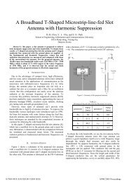
II. ANTENNA DESIGN AND PERFORMANCES<br />
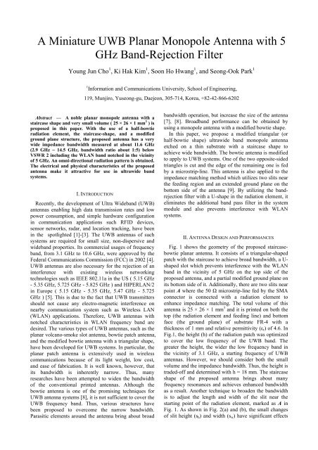
Fig. 1 shows the geometry of the proposed staircasebowtie<br />
planar antenna. It consists of a triangular-shaped<br />
patch <strong>with</strong> the staircase to achieve broad b<strong>and</strong>width, a U-<br />
shaped slot which prevents interference <strong>with</strong> the WLAN<br />
b<strong>and</strong> in the vicinity of 5 GHz on the top side of the<br />
proposed antenna, <strong>and</strong> a partial modified ground plane on<br />
its bottom side of it. Additionally, there are two slits near<br />
point A where the 50 microstrip-line fed by the SMA<br />
connector is connected <strong>with</strong> a radiation element to<br />
enhance impedance matching. The total volume of this<br />
antenna is 25 × 26 × 1 mm 3 <strong>and</strong> it is printed on both the<br />
top (the radiation element <strong>and</strong> feeding line) <strong>and</strong> bottom<br />
face (the ground plane) of substrate FR-4 <strong>with</strong> a<br />
thickness of 1 mm <strong>and</strong> relative permittivity ( r ) of 4.6. In<br />
Fig.1, the height (h) of the radiation patch was optimized<br />
to cover the low frequency of the <strong>UWB</strong> b<strong>and</strong>. The<br />
greater the height, the wider the low frequency b<strong>and</strong> in<br />
the vicinity of 3.1 GHz, a starting frequency of <strong>UWB</strong><br />
antennas. However, we should consider both the small<br />
volume <strong>and</strong> the impedance b<strong>and</strong>width. Thus, the height is<br />
traded-off <strong>and</strong> determined <strong>with</strong> h = 18 mm. The staircase<br />
shape of the proposed antenna brings about many<br />
frequency resonances <strong>and</strong> achieves enhanced b<strong>and</strong>width<br />
as a result. Another technique to broaden the b<strong>and</strong>width<br />
is to adjust the length <strong>and</strong> width of the slit near the<br />
starting point of the radiation element, marked as A in<br />
Fig. 1. As shown in Fig. 2(a) <strong>and</strong> (b), the small changes<br />
of slit height (s h ) <strong>and</strong> width (s w ) have significant effects
(a)<br />
Fig. 1. Geometry of the proposed antenna<br />
(a) Top view (b) Side view (c) Bottom view<br />
on the b<strong>and</strong>width of the proposed antenna. This is<br />
because stronger current distributions – more than any<br />
other region of the radiation element – exist in the<br />
vicinity of point A on the radiation element. Therefore,<br />
that region plays an important role in impedance<br />
matching. In other word, it is a sensitive part of the<br />
tuning region. The optimized value of s h is selected as 2.2<br />
mm, as shown in Fig. 2(a). On the other h<strong>and</strong>, the<br />
b<strong>and</strong>width is further widened when the slit width (s w ) is<br />
narrower, as shown in Fig. 2(b). Nevertheless, the slit<br />
width of s w is determined at 0.2 mm due to the<br />
manufacturing tolerance. In Fig. 1(c), the modified<br />
ground plane is shown on the bottom side of the substrate.<br />
Both side edges of the ground plane were constructed in<br />
a circular shape which consists of a quadrant <strong>with</strong> a<br />
radius of 7 mm in order to reduce the beam tilting <strong>and</strong> to<br />
obtain wide b<strong>and</strong>width [10],[11]. The radiation pattern of<br />
the monopole antenna is not the same as that of the<br />
dipole antenna because it does not an infinite ground<br />
plane. The size of ground plane is finite in actual usage.<br />
The direction of maximum radiation tilts somewhat<br />
upwards from the horizontal plane due to the finite<br />
ground plane. To reduce this beam tilting, the ground<br />
plane of the proposed antenna is designed to have a<br />
circular shape rather than a rectangular shape. To achieve<br />
wider b<strong>and</strong>width, some upper part of the ground plane is<br />
extended [9]. As shown in Fig. 3(a), the small changes in<br />
(b)<br />
Fig. 2. Simulated VSWR as a result of the parameters of each<br />
slit<br />
(a) Variations of s h <strong>with</strong> a fixed value of s w = 0.2 mm<br />
(b) Variations of s w <strong>with</strong> a fixed value of s h = 2.2 mm<br />
the height of the extended ground plane (g h ) has an effect<br />
on the b<strong>and</strong>width of the proposed antenna. But the width<br />
changes have a negligible influence, as shown in Fig.<br />
3(b). The reason is that the extended ground plane is<br />
located in the opposite side of the sensitive point where<br />
the current distribution is the strongest. As in the<br />
preceding explanation, the changes of height (g h ) of the<br />
extended ground plane have significant effects on<br />
impedance matching. Additionally, the extended ground<br />
plane reinforces capacitance. The reinforced capacitance<br />
that results from the extended ground plane cancels the<br />
inductance of the antenna [9]. However, the width<br />
variation of the extended ground plane does not affect the<br />
b<strong>and</strong>width quiet as much because although the width is<br />
wider, the geometry of its sensitive area is almost<br />
constant. The values of g h <strong>and</strong> g w are optimized at 8 mm<br />
<strong>and</strong> 11 mm, respectively. Fig. 4 shows that the U-shaped<br />
slot plays a role in the b<strong>and</strong>-rejection filter. It is<br />
necessary to notch out portions of the b<strong>and</strong> to avoid<br />
interference <strong>with</strong> existing wireless networking<br />
technologies such as IEEE 802.11a. The ability to<br />
provide this function in the antenna can relax the<br />
requirements imposed upon the filtering electronics<br />
<strong>with</strong>in the wireless device. In Fig. 4 (a) <strong>and</strong> (b), there are<br />
similar variations of in each graph. This means that the<br />
resonant frequency of a notched b<strong>and</strong> is determined by
(a)<br />
(a)<br />
(b)<br />
Fig. 3. Simulated VSWR as a result of the parameters of each<br />
extended ground plane<br />
(a) Variations of g h <strong>with</strong> a fixed value of g w = 11 mm<br />
(b) Variations of g w <strong>with</strong> a fixed value of g h = 8 mm<br />
the total length of the slot, not the geometry. The shorter<br />
the total length of the U-shaped slot, the higher the<br />
resonant frequency. The optimized values of f h <strong>and</strong> f w are<br />
6.5 mm <strong>and</strong> 7 mm, respectively. To underst<strong>and</strong> the<br />
behavior of the antenna model <strong>and</strong> obtain the optimum<br />
parameters, simulations were performed <strong>with</strong> the CST<br />
MWS (<strong>Microwave</strong> Studio) based on the Finite<br />
Integration Method. The optimized values of each<br />
physical dimension of the proposed antenna are shown in<br />
Fig. 1 <strong>and</strong> Table I.<br />
III. RESULT<br />
The measured <strong>and</strong> simulated VSWR values in terms of<br />
frequency are compared in Fig. 5. The measured<br />
impedance b<strong>and</strong>width (VSWR 2) is about 11.6 GHz<br />
starting from 2.9 GHz to 14.5 GHz including the notched<br />
b<strong>and</strong>s of the IEEE 802.11a in the US <strong>and</strong> the<br />
HIPERLAN/2 in Europe, <strong>and</strong> its b<strong>and</strong>width ratio is about<br />
1:5. Fig. 5 also shows the measured value <strong>with</strong>out the U-<br />
shaped slot filter. When the slot is omitted, the notched<br />
b<strong>and</strong> is removed. The notched b<strong>and</strong>width of a measured<br />
value is 860 MHz from 5 GHz to 5.86 GHz. The<br />
measured <strong>and</strong> simulated radiation patterns of the<br />
proposed antenna at 7 GHz are plotted in Fig. 6. The<br />
(b)<br />
Fig. 4. Simulated VSWR as a result of the parameters of each<br />
inserted b<strong>and</strong>-notched filter<br />
(a) Variations of f h <strong>with</strong> a fixed value of f w = 7 mm<br />
(b) Variations of f w <strong>with</strong> a fixed value of f h = 6.5 mm<br />
proposed antenna has an acceptable omni-directional<br />
radiation pattern. This shows that the measured <strong>and</strong><br />
simulated results agree well <strong>with</strong> each other. Fig. 7<br />
shows the measured maximum gain of the proposed<br />
antenna <strong>with</strong> <strong>and</strong> <strong>with</strong>out a U-shaped slot filter. A sharp<br />
decrease of maximum antenna gain in the notched<br />
frequency b<strong>and</strong> at 5.5GHz is shown. For other<br />
frequencies outside the notched frequency b<strong>and</strong>, the<br />
antenna gain <strong>with</strong> a filter is similar to those <strong>with</strong>out it.<br />
All measured results are performed <strong>with</strong> an Agilent<br />
8510C network analyzer.<br />
h 18<br />
s h 2.2<br />
s w 0.2<br />
g h 8<br />
g w 11<br />
f h 6.5<br />
f w 7<br />
Unit: mm<br />
TABLE I<br />
OPTIMIZED VALUE OF EACH PARAMETER
Fig. 5. Measured <strong>and</strong> simulated results of VSWR<br />
IV. CONCLUSION<br />
A planar monopole triangular (or half-bowtie shape)<br />
antenna <strong>with</strong> a staircase shape <strong>and</strong> a b<strong>and</strong>-rejection filter<br />
is proposed. In this paper, we investigated the tuning<br />
parameters affected by antenna performances. The area<br />
near point A where current distributions are strong is a<br />
sensitive part of the tuning point. Capacitance <strong>and</strong><br />
inductance can be easily controlled by the extended<br />
ground plane <strong>and</strong> two slits in the vicinity of point A,<br />
respectively. By adjusting them, a wide impedance<br />
b<strong>and</strong>width can be achieved. Additionally, the staircase<br />
shape also helps to enhance impedance b<strong>and</strong>width. The<br />
total length of the U-shaped filter determines the center<br />
frequency of the notched WLAN b<strong>and</strong>. The proposed<br />
antenna has attractive features such as very small volume,<br />
wide impedance b<strong>and</strong>width, WLAN b<strong>and</strong> rejection,<br />
omni-directional radiation pattern, <strong>and</strong> reasonable gain.<br />
Fig. 6. Measured <strong>and</strong> simulated radiation patterns for the<br />
proposed antenna at 7 GHz.<br />
(a) x-y plane. (b) x-z plane. (c) y-z plane.<br />
Fig. 7. Measured gains of the antennas <strong>with</strong> <strong>and</strong> <strong>with</strong>out the U-<br />
shaped slot filter<br />
ACKNOWLEDGEMENT<br />
This work was supported by the National Research<br />
Lab. (NRL) of Ministry of Science <strong>and</strong> Technology,<br />
Korea, under contract no. M1-0203-0015.<br />
REFERENCES<br />
[1] Schantz H.G., “Bottom fed planar elliptical <strong>UWB</strong><br />
antennas”, Proc. IEEE Conf. on Ultra Wideb<strong>and</strong> Systems<br />
<strong>and</strong> Technologies, Reston, VA, USA, 2003<br />
[2] Chen Z.N. <strong>and</strong> Chia M.Y.W., “Impedance characteristics<br />
of trapezoidal planar monopole antenna”, Microw. Opt.<br />
Technol. Lett., 2000, 36, (13), pp. 120–122<br />
[3] Ammann M.J., “The pentagonal planar monopole for<br />
digital mobile terminals; b<strong>and</strong>width considerations <strong>and</strong><br />
modeling”. Proc. IEEE <strong>Antenna</strong>s Propagation Society Int<br />
Symp. Dig., Boston, MA, USA, 2001, Vol. 1, pp. 170–173<br />
[4] FCC 1st Report <strong>and</strong> Order on Ultra-Wideb<strong>and</strong> Technology,<br />
Feb. 2002.<br />
[5] A. Kerkhoff <strong>and</strong> H.Ling, “Design of a <strong>Planar</strong> <strong>Monopole</strong><br />
<strong>Antenna</strong> for Use <strong>with</strong> Ultra-Wideb<strong>and</strong> (<strong>UWB</strong>) Having a<br />
B<strong>and</strong>-Notched Characteristic”, IEEE In17 Symposium on<br />
<strong>Antenna</strong>s <strong>and</strong> Propagation, Columbus, OH, vol. I, pp. 830-<br />
833, June, 2003.<br />
[6] C.A. Balanis, <strong>Antenna</strong> theory: Analysis <strong>and</strong> design. Wiley,<br />
New York, 1997, 441–449<br />
[7] .M. Ali, M. Okoniewki, M.A. Stuchly, <strong>and</strong> S.S. Stuchly,<br />
“Dual-frequency strip-sleeve monopole for laptop<br />
computers”, IEEE Trans <strong>Antenna</strong>s Propagat, 47 (1999),<br />
317–323.<br />
[8] S.D. Rogers <strong>and</strong> C.M. Butler, “The sleeve-cage monopole<br />
<strong>and</strong> helix for wideb<strong>and</strong> operation”, <strong>Antenna</strong>s <strong>and</strong><br />
Propagation Society, IEEE International Symposium, 1999,<br />
Vol. 2, pp. 1308–1311.<br />
[9] Jong-Pil Lee, Seong-Ook Park, <strong>and</strong> Sang-Keun Lee, “Bowtie<br />
Wide-b<strong>and</strong> <strong>Monopole</strong> <strong>Antenna</strong> <strong>with</strong> the novel<br />
Impedance-matching Technique”, Microw. Opt. Technol.<br />
Lett., 2002, 33, (6), pp. 448–452<br />
[10] Hahn, R. F. <strong>and</strong> J. G. Fikioris, "Impedance <strong>and</strong> radiation<br />
pattern of antennas above flat discs.",IEEE Trans.<br />
<strong>Antenna</strong>s <strong>and</strong> propagation, vol. Ap-21, no. 1, pp. 97-100,<br />
Jan. 1973.<br />
[11] H.K Yoon, H. R Kim, K. H. Chang, Y. J. Yoon <strong>and</strong> Y. H.<br />
Kim, "A Study on the <strong>UWB</strong> <strong>Antenna</strong> <strong>with</strong> B<strong>and</strong>-rejection<br />
Characteristic", IEEE, <strong>Antenna</strong>s <strong>and</strong> Propagation Society<br />
Symposium, June 2004 Page(s):1784 - 1787 Vol.2