Design and Analysis of Ultrasonic NDT Instrumentation ... - IJME
Design and Analysis of Ultrasonic NDT Instrumentation ... - IJME
Design and Analysis of Ultrasonic NDT Instrumentation ... - IJME

You also want an ePaper? Increase the reach of your titles
YUMPU automatically turns print PDFs into web optimized ePapers that Google loves.
DESIGN AND ANALYSIS OF ULTRASONIC <strong>NDT</strong><br />
INSTRUMENTATION THROUGH SYSTEM MODELING<br />
——————————————————————————————————————————————–————<br />
T. Parthipan, Brunel University; P. Mudge, TWI Ltd.; R. Nilavalan, Brunel University; W. Balach<strong>and</strong>ran, Brunel University<br />
Abstract<br />
System modeling techniques were used to perform a power<br />
analysis <strong>of</strong> a battery-operated non-destructive testing system<br />
to reliably predict the required power source for the<br />
system. Topology-specific <strong>and</strong> equivalent circuit models<br />
written in SPICE were employed for modeling this multiengineering<br />
discipline system. Crucial system constraints<br />
such as power consumption <strong>and</strong> power dissipation were<br />
simulated <strong>and</strong> evaluated. Presented here is the modeling<br />
work carried out on the electromechanical load, excitationcircuits<br />
<strong>and</strong> high-voltage power supply. Simulation schematics<br />
were translated into hardware schematics <strong>and</strong> prototyped.<br />
Measurements on prototyped hardware are also presented<br />
for comparison with simulation results <strong>and</strong> model<br />
evaluation. Close mapping <strong>of</strong> simulation results to real hardware<br />
was obtained for topology-specific models; agreement<br />
within 20% was achieved for equivalent circuit models. The<br />
system model developed in this study is currently being<br />
used as a virtual test platform for verifying various design<br />
methodologies <strong>and</strong> foreseeing uncertainties.<br />
such as defects <strong>and</strong> reflect back to the same transducer that<br />
captures the echo signal [2].<br />
To date, the most common application <strong>of</strong> LRUT is in the<br />
in-situ inspection <strong>of</strong> industrial pipelines [1], [2]. The effectiveness<br />
<strong>and</strong> the economic viability <strong>of</strong> the LRUT method led<br />
industry to broaden its applications to include condition<br />
monitoring <strong>of</strong> large remote structures or those with limited<br />
access for maintenance such as <strong>of</strong>fshore wind-farm turbine<br />
towers, tanks <strong>and</strong> floating production storage <strong>and</strong> <strong>of</strong>floading<br />
vessels (FPSOs). These applications require remotely<br />
installed, distributed-sensor networks based on the LRUT<br />
technique.<br />
Introduction<br />
Structures which are installed <strong>and</strong> operate in harsh environments<br />
in extreme conditions are likely to fail prematurely.<br />
Reliable structural monitoring instrumentation is crucial<br />
for monitoring the condition <strong>of</strong> these structures. Long<br />
Range <strong>Ultrasonic</strong> Testing (LRUT) is a novel nondestructive<br />
testing (<strong>NDT</strong>) method used in the detection <strong>of</strong><br />
volumetric defects such as gross corrosion [1].<br />
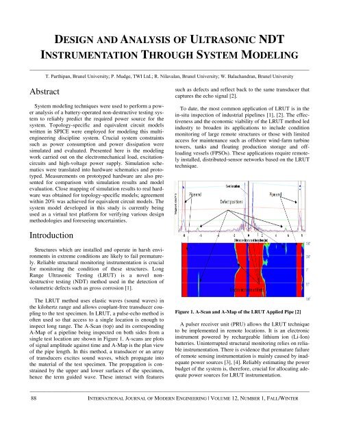
The LRUT method uses elastic waves (sound waves) in<br />
the kilohertz range <strong>and</strong> allows couplant-free transducer coupling<br />
to the test specimen. In LRUT, a pulse-echo method is<br />
<strong>of</strong>ten used so that access to a single location is enough to<br />
inspect long range. The A-Scan (top) <strong>and</strong> its corresponding<br />
A-Map <strong>of</strong> a pipeline being inspected on both sides from a<br />
single test location are shown in Figure 1. A-scans are plots<br />
<strong>of</strong> signal amplitude against time <strong>and</strong> A-Map is the plan view<br />
<strong>of</strong> the pipe length. In this method, a transducer or an array<br />
<strong>of</strong> transducers excites sound waves, which propagate into<br />
the material <strong>of</strong> the test specimen. The propagation is constrained<br />
by the upper <strong>and</strong> lower surfaces <strong>of</strong> the specimen,<br />
hence the term guided wave. These interact with features<br />
Figure 1. A-Scan <strong>and</strong> A-Map <strong>of</strong> the LRUT Applied Pipe [2]<br />
A pulser receiver unit (PRU) allows the LRUT technique<br />
to be implemented in remote locations. It is an electronic<br />
instrument powered by rechargeable lithium ion (Li-Ion)<br />
batteries. Uninterrupted structural monitoring relies on reliable<br />
instrumentation. There is evidence that premature failure<br />
<strong>of</strong> remote sensing instrumentation is mainly caused by inadequate<br />
power sources [3], [4]. Reliably estimating the power<br />
budget <strong>of</strong> the system is, therefore, crucial for allocating adequate<br />
power sources for LRUT instrumentation.<br />
——————————————————————————————————————————————–————<br />
88 INTERNATIONAL JOURNAL OF MODERN ENGINEERING | VOLUME 12, NUMBER 1, FALL/WINTER
——————————————————————————————————————————————–————<br />
Power consumption can vary for different functions <strong>and</strong><br />
scenarios. Power analysis on LRUT hardware for various<br />
scenarios <strong>and</strong> functionalities can enable one to specify an<br />
adequate power source for the instrumentation that would<br />
last for the scheduled inspection period. However, practical<br />
experimentation using hardware is not always possible at<br />
early stages <strong>of</strong> the project, nor is it feasible to run such experiments<br />
for all scenarios. Computer system modeling <strong>of</strong><br />
the LRUT system forms a virtual test platform that can be<br />
used for power analysis <strong>and</strong> optimization without the need<br />
for any hardware.<br />
System Modeling Concept<br />
Accurately modeling the inter-coupling nature between<br />
different engineering disciplines <strong>and</strong> simultaneously simulating<br />
the constructs on a single platform is crucial for underst<strong>and</strong>ing<br />
the system. There are high-end tools such as<br />
Saber <strong>and</strong> System-Vision from Cadence <strong>and</strong> Mentor<br />
graphics, respectively, which allow multi-engineering discipline<br />
systems to be modeled <strong>and</strong> simulated on a single platform,<br />
but they require specialized knowledge in all relevant<br />
engineering disciplines. The cost <strong>of</strong> licensing these tools is<br />
also high <strong>and</strong> disproportionate to most project costs. Computing<br />
power requirement is also intense.<br />
The LRUT System Model<br />
The simplified version <strong>of</strong> the LRUT system model using<br />
LTSpice is shown in Figure 2. It includes several constructs<br />
such as transmit circuit, transmit/receive transducer array<br />
(PZT_Array), test specimen (Pipeline) <strong>and</strong> receive circuit<br />
(Preamp). The system model represents a pulse-echo mode<br />
<strong>of</strong> operation. The pipeline was modeled using a lossy transmission<br />
line model. It has an integrated feature (e.g. defectweld<br />
– acoustic impedance mismatch) <strong>and</strong> the pipe end is<br />
terminated at an acoustic impedance equivalent to air. Each<br />
transducer in the transducer array is damped with a stainless<br />
steel backing block; more details are given in the load characterization<br />
section. This LRUT system model not only<br />
allows for analysis <strong>of</strong> the power performance <strong>of</strong> the system,<br />
but also allows port dynamics to be analyzed for signal<br />
strength.<br />
<strong>Ultrasonic</strong> piezoelectric transducers (lead-zirconatetitanate<br />
- PZT) are <strong>of</strong>ten used as transmit <strong>and</strong> receive sensors<br />
in LRUT techniques. The capacitive nature <strong>of</strong> these<br />
PZTs requires a high-voltage stress (excitation voltage) to<br />
force them into oscillation <strong>and</strong> to achieve a high signal-tonoise<br />
ratio. This high excitation voltage signal needs to be<br />
short (broadb<strong>and</strong>) in order to achieve better resolution [7-9].<br />
SPICE is a computer modeling language, which allows<br />
equivalent circuit models <strong>of</strong> different engineering disciplines<br />
to be modeled in the electronic domain. LTSpice is a<br />
free SPICE-based simulation tool developed by power product<br />
company Linear-Technology. It allows models to be<br />
inputted with their relevant parameters <strong>and</strong> simulated simultaneously<br />
on a single simulation platform. This method requires<br />
minimal knowledge <strong>of</strong> other secondary engineering<br />
disciplines, <strong>and</strong> simulation time <strong>and</strong> computing power are<br />
affordable, due to the simplistic algorithms <strong>and</strong> relaxed parameters.<br />
The LRUT system consists <strong>of</strong> multi-engineeringdiscipline<br />
constructs such as electrochemical (battery model),<br />
electromechanical (transducers - load) <strong>and</strong> analogdigital<br />
mixed-signal electrical components. SPICE-language<br />
-based equivalent circuit models have been developed for<br />
simulating foreign domain constructs in SPICE-based simulation<br />
tools [5], [6]. However, there is a trade <strong>of</strong>f in the accuracy<br />
<strong>of</strong> equivalent circuit model simulation results compared<br />
with the real system. Topology-specific models have<br />
been used in modeling work for power <strong>and</strong> functionally<br />
sensitive constructs. Presented here is the modeling <strong>and</strong><br />
related practical work carried out on the load, transmitcircuit<br />
<strong>and</strong> the high-voltage power supply in the associated<br />
system that has significant influence on power performance.<br />
Figure 2. Simplified LRUT System Model Constructed in<br />
LTSpice<br />
——————————————————————————————————————————————————-<br />
DESIGN AND ANALYSIS OF ULTRASONIC <strong>NDT</strong> INSTRUMENTATION THROUGH SYSTEM MODELING 89
——————————————————————————————————————————————–————<br />
The LRUT application uses a 240V pk-pk electrical signal in<br />
the frequency range <strong>of</strong> 20kHz to 100kHz. The technique<br />
requires a number <strong>of</strong> excitations (<strong>and</strong> data collection) at a<br />
repetitive rate (rep-rate) <strong>of</strong> 0.1s for data manipulation. The<br />
main circuits involved are the transmit-circuit (TX), receive<br />
-circuit (RX), high-voltage power supply (CCPS) <strong>and</strong> the<br />
digital logic control circuits (DSP). The TX circuit produces<br />
a high-voltage, high-current electrical signal that excites the<br />
transducer array (load) that in turn produces the sound<br />
waves. The receive-circuit allows reception <strong>and</strong> signal processing<br />
<strong>of</strong> the echo signals from features. CCPS is a fast<br />
capacitor-charging power supply that produces +/-150V on<br />
dem<strong>and</strong>, which provides voltage to the TX. The DSP h<strong>and</strong>les<br />
system control, signal processing, storage <strong>and</strong> communication.<br />
Load characterization<br />
Load charecterisation is required for specifying the PRU’s<br />
port dynamics <strong>and</strong> power performance. Load for the PRU is<br />
an array <strong>of</strong> PZT transducers <strong>of</strong> the type EBL#2 [10] that are<br />
pre-engineererd with damping blocks <strong>and</strong> faceplates. A<br />
number <strong>of</strong> equivalent circuit models for PZT transducers are<br />
discussed in the literatue [5]. This work employed a singledimensional-thickness<br />
mode Krimholtz, Leedom <strong>and</strong><br />
Matthaei (KLM) model, as the KLM model allows<br />
additional layers such as face plates <strong>and</strong> matching layers to<br />
be easily added on to the model. Faceplates <strong>and</strong> matching<br />
layers can be modelled using the lossy transmission-line<br />
model. The derivation <strong>of</strong> parameters used in the KLM model<br />
for the PZT transducer requires three basic parameters<br />
that can only be obtained using practical measurements or<br />
by using equations [11]. They are free capacitance (C T ),<br />
resonant frequency (f p ) <strong>and</strong> anti-resonant frequency (f a ) <strong>of</strong><br />
the transducer. A Solartron SI1260 impedance analyzer was<br />
used for the practical impedance analysis. The measured<br />
free capacitance was approximately 1100pF at an excitation<br />
frequency <strong>of</strong> 1kHz. The resonant frequency (f p ) <strong>and</strong> antiresonant<br />
frequency (f a ) were measured as 1.7MHz <strong>and</strong><br />
2.4MHz, respectively. Another study claimed that for transducers<br />
having a thickness very much smaller than the other<br />
dimensions, the vibrations in directions other than thickness<br />
are insignificant for modeling purposes [12]. Hence, this<br />
single-dimensional model is adequate for the modeling process<br />
considered here.<br />
Practical input-impedance analysis results were compared<br />
with the simulation results across the frequency range <strong>of</strong><br />
interest. Figure 3 compares the simulation <strong>and</strong> practical<br />
results obtained for a single PZT. Impedance <strong>and</strong> phase<br />
graphs are set to show 20% <strong>and</strong> 2% error bars, respectively.<br />
A good agreement within 20% was obtained between the<br />
simulation <strong>and</strong> practical results.<br />
Impedance (Ω)<br />
1.00E+04<br />
9.00E+03<br />
8.00E+03<br />
7.00E+03<br />
6.00E+03<br />
5.00E+03<br />
4.00E+03<br />
3.00E+03<br />
2.00E+03<br />
1.00E+03<br />
0.00E+00<br />
1.00E+04<br />
2.00E+04<br />
3.00E+04<br />
Input impedance analysis<br />
(Single ELB#2 transducer)<br />
4.00E+04<br />
5.00E+04<br />
6.00E+04<br />
1.000E+05,<br />
1.699E+03<br />
1.065E+05,<br />
1.369E+03<br />
Figure 3. Input Impedance <strong>Analysis</strong> <strong>of</strong> a Single Domain PZT<br />
7.00E+04<br />
In LRUT applications, PZT elements are mounted to<br />
stainless steel backing blocks for damping <strong>and</strong> mounting<br />
purposes. This transducer fabrication also includes a faceplate<br />
for acoustic impedance matching <strong>and</strong> durability. The<br />
PZT transducer with backing block <strong>and</strong> faceplate is called<br />
an LRUT transducer. Each output port in the PRU system is<br />
specified to drive an array <strong>of</strong> LRUT transducers. The array<br />
size can be as big as 13 LRUT transducers connected in<br />
parallel.<br />
The total input impedance analysis for an array <strong>of</strong> 13<br />
LRUT transducers was also carried out practically <strong>and</strong><br />
through computer simulations. Faceplates were modeled<br />
using a transmission-line model. The stainless steel dampers<br />
were modeled with resisters, whose values were calculated<br />
using the acoustic impedance formula, R =ρAu p , where ρ, A<br />
<strong>and</strong> u p were the density <strong>of</strong> stainless steel, cross sectional<br />
area <strong>and</strong> phase velocity, respectively [13]. The practical <strong>and</strong><br />
simulated results are shown in Figure 4. Discrepancies within<br />
30% were observed between practical <strong>and</strong> simulation<br />
results. As the operating region <strong>of</strong> the LRUT application<br />
was well below the series resonance frequency <strong>of</strong> the PZTs,<br />
the load held capacitive properties as expected [11]. This<br />
can be seen in Figure 3, where the phase angles are around<br />
negative 90 degrees (-90°).<br />
A maximum <strong>of</strong> 40% variation in input capacitance was<br />
observed when practical tests were carried out on two batches<br />
<strong>of</strong> 77 transducers (within <strong>and</strong> between the batches).<br />
Hence, the 30% discrepancy observed in Figure 4 was acceptable.<br />
It was concluded from the modeling work that the<br />
minimum value <strong>of</strong> load impedance was 115Ω±30%<br />
(80.5Ω), which was confirmed through practical results.<br />
8.00E+04<br />
Excitation frequency (kHz)<br />
Impedance - Practical<br />
Phase - Practical<br />
9.00E+04<br />
1.00E+05<br />
1.10E+05<br />
-82<br />
-88<br />
-94<br />
-100<br />
Phase (°)<br />
Impedance - Simulation<br />
Phase - Simulation<br />
——————————————————————————————————————————————–————<br />
90 INTERNATIONAL JOURNAL OF MODERN ENGINEERING | VOLUME 12, NUMBER 1, FALL/WINTER 2011
——————————————————————————————————————————————–————<br />
Impedance (Ω)<br />
Input impedance analysis<br />
(Array <strong>of</strong> 13 LRUT transducers clamped <strong>and</strong> unclamped to medium)<br />
8.E+02<br />
6.E+02<br />
4.E+02<br />
2.E+02<br />
1.E+01<br />
0.E+00<br />
1.E+04<br />
2.E+04<br />
3.E+04<br />
4.E+04<br />
Figure 4. Input Impedance <strong>Analysis</strong> <strong>of</strong> an Array <strong>of</strong> 13 PZT<br />
5.E+04<br />
6.E+04<br />
7.E+04<br />
Excitation frequency (kHz)<br />
Impedance_Unclamped - Practical impedance_Clamped - Practical<br />
Impedance_Unclamped - Simulation Impedance_Clamped - Simulation<br />
8.E+04<br />
9.E+04<br />
1.E+05<br />
A complementary MOSFET arrangement, as shown in<br />
Figure 5, can provide the required high slew rate, highvoltage<br />
excitation waveform <strong>and</strong> load current dem<strong>and</strong>. The<br />
circuit arrangement consists <strong>of</strong> a single, high-voltage power<br />
amplifier (PA) <strong>and</strong> high-voltage N-type <strong>and</strong> P-type metaloxide<br />
semiconductor field-effect transistors (MOSFET).<br />
The complementary MOSFET arrangement acts as a current<br />
source <strong>and</strong> provides the required load current that the highvoltage<br />
PA cannot provide alone. Steele <strong>and</strong> Eddlemon [16]<br />
provide a detailed operation <strong>of</strong> the circuit. Resistor R gs was<br />
chosen to guarantee the maximum required V gs (obtained<br />
from MOSFETs datasheets) for the MOSFETs with the PA<br />
output current limit [15]. The added auxiliary circuits provide<br />
circuit <strong>and</strong> load protection. The combination <strong>of</strong> U2-Q1-<br />
Rcl+ <strong>and</strong> U3-Q2-Rcl- provides the current limit protection<br />
in the event that the load current exceeds the maximum load<br />
current <strong>of</strong> 1.5A. R6 is a high-value resistor, which provides<br />
additional protection for the PA (limits the PA output current),<br />
should the MOSFETs open. D1 <strong>and</strong> D2 are zener diodes<br />
that limit the V gs to the maximum specified V gs .<br />
0<br />
R4<br />
V1 - +<br />
NMOS<br />
Transmit Circuit<br />
A transmit circuit capable <strong>of</strong> exciting a capacitive load<br />
with an equivalent impedance <strong>of</strong> 80.5Ω (70% <strong>of</strong> the 115Ω<br />
for the minimum stated above) was modeled, simulated <strong>and</strong><br />
prototyped. Using the TX circuit specifications shown in<br />
Table 1, design constraints such as slew rate, peak load current<br />
<strong>and</strong> the instantaneous power consumption <strong>of</strong> the circuit<br />
were calculated as 75.3V/µs, 1.5A <strong>and</strong> 178W, respectively<br />
[14], [15].<br />
VIN<br />
C1<br />
R8<br />
R7<br />
PowerAmp<br />
5 7<br />
1<br />
V-CL<br />
10<br />
-<br />
OUT<br />
2<br />
9<br />
+<br />
8<br />
U1 V+<br />
CMP2<br />
6<br />
CMP1<br />
Rcl+<br />
D1 D2<br />
Rgs<br />
Rcl-<br />
Q1<br />
2 1<br />
5 4<br />
TO LOAD<br />
R6<br />
0<br />
U2<br />
Table 1. Transmit Circuit Specification<br />
Parameter Symbol Range<br />
Tx Supply Voltage +Vs <strong>and</strong> -Vs ±150Vdc<br />
Excitation signal frequency F exc<br />
20kHz-<br />
100kHz<br />
Load Value Z total 115Ω±30%<br />
Excitation Voltage V exc ±120Vpk<br />
Input signal Vin 1Vpk-pk<br />
Inverting fixed gain G 150(43dB)<br />
Number <strong>of</strong> sine waves per<br />
transmit envelop<br />
N cycle Max 20<br />
Min 10<br />
Figure 5. Transmit Circuit<br />
0<br />
V2 + -<br />
PMOS<br />
A number <strong>of</strong> simulations were carried out on this circuit<br />
to evaluate stability, SR <strong>and</strong>, most importantly, power consumption<br />
<strong>and</strong> dissipation at the component level. Simulation<br />
results showed that approximately 10% <strong>of</strong> the supply voltage<br />
drops across the MOSFETs <strong>and</strong> the PA during excitation,<br />
generating heat, thus requiring heat sinks. Figure 6<br />
shows the power performance <strong>of</strong> the circuit for the heaviest<br />
load (80.5Ω). It can be seen that the peak instantaneous<br />
power consumption <strong>of</strong> the transmit circuit is about 200W at<br />
the excitation frequency <strong>of</strong> 100kHz for the aforementioned<br />
——————————————————————————————————————————————————-<br />
DESIGN AND ANALYSIS OF ULTRASONIC <strong>NDT</strong> INSTRUMENTATION THROUGH SYSTEM MODELING 91<br />
0<br />
R5<br />
Q2<br />
2 1<br />
5 4<br />
U3
——————————————————————————————————————————————–————<br />
load characteristics. High current <strong>and</strong> voltage spikes at the<br />
rising edge <strong>of</strong> the waveforms are due to the short-circuit<br />
behavior <strong>of</strong> the capacitive load at the initial stage (before<br />
charging). The quiescent current <strong>of</strong> the PA was about 10mA<br />
[15]; for the applied potential <strong>of</strong> 300V pk-pk , the quiescent<br />
power consumption <strong>of</strong> the circuit was about 3W. This is<br />
also noticeable in Figure 6. The simulation results for power<br />
consumption were higher than the calculated value (177W)<br />
as the calculation steps did not account for power consumption<br />
<strong>and</strong> losses in the auxiliary components. The results presented<br />
in Figure 6 also show that the load current was 1.5A<br />
at a frequency <strong>of</strong> 100kHz.<br />
Power Consumption (W)<br />
1000<br />
100<br />
10<br />
1<br />
0.00E+00<br />
Transmit Circuit Performance<br />
Power consumption <strong>and</strong> Load current at 100kHz<br />
2.00E-05<br />
4.00E-05<br />
6.00E-05<br />
Excitation frequency (kHz)<br />
8.00E-05<br />
1.00E-04<br />
1.5<br />
1.0<br />
0.5<br />
0.0<br />
-0.5<br />
-1.0<br />
-1.5<br />
Load current (A)<br />
High Voltage Power Supply<br />
Normally, power to this type <strong>of</strong> pulsed load is provided<br />
using bulk capacitor banks. In this scenario, energy is stored<br />
in capacitors <strong>and</strong> discharged to the load upon dem<strong>and</strong>. Topping<br />
<strong>of</strong>f the capacitor bank is required in order to maintain<br />
the voltage between repetitive load pulses. A typical PRU<br />
requires separate capacitor banks for +150V <strong>and</strong> -150V rails<br />
with 1,600µF, totaling 3,200µF.<br />
Push-pull converter topology <strong>and</strong> flyback topology are<br />
commonly used in rapid capacitor-charging processes. Push<br />
-pull topology is generally used in applications where power<br />
requirements are above 200W. A flyback topology was selected<br />
for this application due to its simplicity, size, low<br />
cost <strong>and</strong> its widespread use in power applications requiring<br />
power levels below 200W [17]. A single-stage flyback<br />
CCPS was modeled for meeting the specification <strong>of</strong> charging<br />
a 2x1600 µF capacitor bank within 2s <strong>of</strong> initial dem<strong>and</strong><br />
<strong>and</strong> keeping the +/-150 V supply regulation within 4% <strong>of</strong><br />
target.<br />
The operation <strong>of</strong> flyback power supply is explained in a<br />
report by Basso [17]. The only difference between that work<br />
<strong>and</strong> this study is the split power-supply design. This was<br />
achieved using a center-tap transformer. Figure 7 depicts the<br />
simplified schematic diagram <strong>of</strong> the dual–rail, single-stage<br />
flyback converter circuit. In flyback topology, transformer<br />
T1 is used for maximum energy storage purposes. Hence, it<br />
is built with air gaps in the core to trap the energy in them.<br />
Total Power consumption - 100kHz<br />
Load current - 100kHz<br />
Figure 6. Transmit Circuit Performance<br />
The transmit envelope maximum duration was calculated as<br />
1ms using Equation (1), the values for which are given in<br />
Table 1.<br />
TX = N<br />
duration<br />
cycle<br />
F<br />
exc _min<br />
(1)<br />
The implication <strong>of</strong> Equation (1) is that the energy utilized<br />
by the transmit circuit per transmit cycle is 200mJ (200W x<br />
1ms). A typical PRU can support 24 <strong>of</strong> these loads, hence<br />
24x 200mJ is consumed immediately. A steady power supply<br />
is, therefore, required to provide 200mJ, while maintaining<br />
the power rails at +/-150V (low ripple) for each transmit<br />
cycle.<br />
Figure 7. CCPS based on Flyback Topology<br />
——————————————————————————————————————————————–————<br />
92 INTERNATIONAL JOURNAL OF MODERN ENGINEERING | VOLUME 12, NUMBER 1, FALL/WINTER 2011
——————————————————————————————————————————————–————<br />
When switch Q1 is turned on, the current in the primary<br />
inductor (L 1 ) ramps up with the flux storing magnetic energy.<br />
A voltage is induced across the secondary winding (L2,<br />
L3) <strong>of</strong> a polarity such that D1 <strong>and</strong> D4 are reverse-biased.<br />
Hence, no current flows in the secondary circuit. When Q1<br />
is turned <strong>of</strong>f, the primary current drops to zero <strong>and</strong> the voltage<br />
across secondary windings L1 <strong>and</strong> L2 reverses, allowing<br />
D1 <strong>and</strong> D4 to conduct current that, in turn, charges capacitor<br />
banks C1 <strong>and</strong> C2.<br />
Flyback topology can be used in either discontinuous current<br />
mode (DCM) or continuous current mode (CCM). In<br />
general, low–voltage, high-current applications use CCM<br />
<strong>and</strong> high-voltage applications use DCM. As this is a highvoltage<br />
circuit (transmit current is only drawn from the capacitor<br />
banks), DCM is appropriate, but this method is less<br />
efficient <strong>and</strong> tends to heat up the magnetics <strong>and</strong> the switching<br />
device [17]. Boundary mode (BM) operation is also<br />
appropriate for this application. In BM, the switching current<br />
drops to zero as soon as the switch opens, which make<br />
the CCPS very efficient.<br />
There are a number <strong>of</strong> components which need to be selected<br />
before carrying out topology-specific modeling <strong>and</strong><br />
simulation <strong>of</strong> this CCPS. They were calculated <strong>and</strong> listed in<br />
Table 2 [18]. A correct selection is important in order to<br />
achieve the specified performance.<br />
Simulation results that demonstrate the model fitness <strong>of</strong><br />
the CCPS are presented in this section. Figure 8 shows the<br />
V ds (drain-source voltage) across the switching device, Q1,<br />
where I d is the drain current switching through Q1 when Q1<br />
is turned on. It is clear that the drain <strong>of</strong> the MOSFET is experiencing<br />
an approximate 60V spike due to stray inductance<br />
<strong>and</strong> high di/dt at turn <strong>of</strong>f. The selected MOSFET was<br />
rated at 150V, 5A (pulsed current). The drain current, I d ,<br />
passing through Q1 when switched on was limited to 4A in<br />
the calculation, though the simulation showed that I d could<br />
reach a peak value <strong>of</strong> 4.2A.<br />
Figure 8. Simulated Switching Device Performance<br />
Figure 9 shows the current passing through the output<br />
diode (D1). Average <strong>and</strong> peak diode current values <strong>of</strong><br />
64mA <strong>and</strong> 240mA were observed. This was expected as<br />
calculations indicated that the peak diode current is approximately<br />
I PK /2N, or 200mA. The diodes selected for this application<br />
can h<strong>and</strong>le 1A peak current. A fast Fourier transform<br />
(FFT) <strong>of</strong> the Q1 switching signal was also probed during<br />
simulation to find the maximum switching frequency.<br />
Table 2. Component Rating for CCPS<br />
Component<br />
Transformer inductor<br />
Switching device N-Type<br />
MOSFET<br />
Output diodes – Rectifiers<br />
Peak Primary current (I PRI )<br />
Constrains<br />
Primary Inductance 11µH;<br />
turns ratio 1:10<br />
V BR > 32V; I d-average > 0.94A<br />
V RRM = 320V or better; I F(AV)<br />
> 200mA<br />
The power-source protection circuits in the PRU are specified<br />
to h<strong>and</strong>le the maximum <strong>of</strong> 10A. The PRU has other<br />
circuits that require considerable amounts <strong>of</strong> current while<br />
the capacitor bank is charging. Hence, the primary peak<br />
current (I PRI ) that the CCPS would use during initial charge<br />
up was limited to 4A using R4 in Figure 7.<br />
4A<br />
Figure 9. Simulated Rectifier Diode Current<br />
The results are presented in Figure 10 <strong>and</strong> show Q1 as<br />
being switched on at a maximum switching frequency <strong>of</strong><br />
150kHz. This value was also used to specify the flyback<br />
transformer. For a 20W design, the switching frequency can<br />
be between 100kHz <strong>and</strong> 200kHz [18].<br />
Figure 10. FFT <strong>of</strong> Switching Signal: Q1 Gate Drive Signal<br />
——————————————————————————————————————————————————-<br />
DESIGN AND ANALYSIS OF ULTRASONIC <strong>NDT</strong> INSTRUMENTATION THROUGH SYSTEM MODELING 93
——————————————————————————————————————————————–————<br />
The amount <strong>of</strong> electromagnetic interference (EMI) this<br />
switch-mode power-supply circuit introduces to the PRU<br />
can affect the ultrasonic performance <strong>of</strong> the system. It is<br />
necessary, then, that any EMI within the frequency spectrum<br />
from 20kHz to 100kHz would need to be kept below a<br />
noise value <strong>of</strong> -72dB. Differential-mode (DM) <strong>and</strong> common<br />
-mode (CM) noise were evaluated in the simulation using a<br />
line impedance stabilization network (LISN) at the input<br />
<strong>and</strong> output (not shown). Differential-mode noise is generally<br />
generated due to high di/dt (fast switching) effects on<br />
stray inductance. Common-mode noise is generally due to<br />
dv/dt effects. This can propagate through the PCB tracks.<br />
Localized filtering <strong>and</strong> careful PCB layout are necessary for<br />
noise suppression. Figure 11 depicts the FFT <strong>of</strong> DM (green<br />
trace, top) <strong>and</strong> CM (blue trace, bottom) noise level at the<br />
LISNs inserted at the input stage. Similar work was carried<br />
out on the output stage as well (before the capacitor bank).<br />
Appropriate filtering was included to prevent EMI spreading<br />
to sensitive TX <strong>and</strong> RX circuits.<br />
carried out. Some experimental results are presented to<br />
show the validity <strong>of</strong> the model developed here.<br />
Figure 12. Simulated Boundary Mode Operation <strong>of</strong> CCPS<br />
Figure 13 depicts the practical measurement taken on the<br />
prototyped CCPS for Q1, drain current I d (CH1/R4), output<br />
voltages +150V (CH3), -150V (CH4) <strong>and</strong> the switching<br />
signal (CH2). I d was measured as high as 18A initially <strong>and</strong><br />
then dropped to 4A during charging as set by R4 in Figure<br />
7. The initial 18A surge was <strong>of</strong> short duration <strong>and</strong> can be<br />
tolerated by Q1. In simulation, initial I d values were seen as<br />
high as 26A (not shown in this paper). Maximum switching<br />
frequency was measured as high as 179kHz, as shown in<br />
Figure 14.<br />
Figure 11. FFT <strong>of</strong> Differential <strong>and</strong> Common Mode Noise<br />
Figure 12 highlights the BM-mode operation <strong>of</strong> the efficient<br />
flyback topology. As can be seen, the drain current <strong>of</strong><br />
Q1 (I d ) drops to zero with the Q1 switching signal (V<br />
(n012)), i.e., in BM the primary inductor current (I PRI ) drops<br />
to zero as soon as the switch (Q1) opens, allowing efficient<br />
transfer <strong>of</strong> energy. The efficiency <strong>of</strong> the CCPS circuit was<br />
analyzed through simulation for varying input voltages<br />
(battery voltage) from 13V to 16.8V in 1V steps. Consistent<br />
efficiency <strong>of</strong> 87% was observed for both light <strong>and</strong> heavy<br />
loads.<br />
Practical Validation<br />
Practical results for evaluating the load model were discussed<br />
in the load-characterization section. A prototype <strong>of</strong><br />
the modeled CCPS was produced <strong>and</strong> practical tests were<br />
Figure 13. Performance <strong>of</strong> CCPS - Measured<br />
The voltage stress that the switching device, Q1, experienced<br />
(V ds ) during switching <strong>of</strong>f <strong>and</strong> the mode <strong>of</strong> operation<br />
<strong>of</strong> the CCPS were probed <strong>and</strong> are portrayed in Figure 15. As<br />
can be seen (CH4), the drain voltage, V ds , peaks at 60V<br />
when Q1 switches <strong>of</strong>f. The simulation results depicted in<br />
Figure 8 also predicted similar values for V ds . The choice <strong>of</strong><br />
a 150V breakdown voltage for the MOSFET (Q1) was because<br />
it could h<strong>and</strong>le this voltage stress. The need for a<br />
snubber circuit <strong>and</strong> the unnecessary power dissipation in the<br />
snubber resistor can be avoided by carefully selecting the<br />
——————————————————————————————————————————————–————<br />
94 INTERNATIONAL JOURNAL OF MODERN ENGINEERING | VOLUME 12, NUMBER 1, FALL/WINTER 2011
——————————————————————————————————————————————–————<br />
device <strong>and</strong> keeping the PCB tracks short. BM operation is<br />
maintained as the drain current <strong>of</strong> Q1 (CH1) drops down to<br />
zero when Q1 is turned <strong>of</strong>f (switching signal - CH2). Other<br />
CCPS-related practical results validating the model were<br />
obtained, but are not included here.<br />
Figure 16. Transmit Circuit Output - Measured<br />
Power Budgeting<br />
Figure 14. Maximum Switching Frequency <strong>of</strong> Q1<br />
A typical power-consumption pr<strong>of</strong>ile for the modelled<br />
LRUT system for one complete inspection cycle (test) was<br />
predicted using simulation. A SPICE-based equivalent circuit<br />
model <strong>of</strong> a Li-Ion battery pack was used as a power<br />
source for the simulation [6]. The simulation data was used<br />
to obtain the adequate power-source capacity value. For<br />
both simulation <strong>and</strong> live measurements, Figure 17 shows<br />
how the power source (battery) terminal voltage drops according<br />
to the number <strong>of</strong> tests. The cut-<strong>of</strong>f terminal voltage<br />
<strong>of</strong> a series-connected 4-cell 3.3V (nominal volts) Li-Ion<br />
battery pack is about 12V, meaning that the maximum number<br />
<strong>of</strong> complete tests that can be carried out before the likelihood<br />
<strong>of</strong> system failure due to lack <strong>of</strong> power is 12.<br />
Hardware Realization<br />
Figure 15. Performance <strong>of</strong> Q1 <strong>and</strong> BM Operation<br />
The transmit circuit excitation signal <strong>of</strong> voltage +/-140V<br />
at 50kHz is shown in Figure 16, revealing no cross distortion<br />
or slew rate limitation. A voltage drop <strong>of</strong> 20V across<br />
the PA <strong>and</strong> the MOSFETs <strong>of</strong> the transmit circuit (Figure 5)<br />
was noticed when a +/-150V excitation pulse was dem<strong>and</strong>ed<br />
at the transmit circuit output, thereby causing voltage clipping<br />
at +/-140V.<br />
A commercial product was manufactured based on the<br />
modeling <strong>and</strong> the prototype <strong>and</strong> launched at the American<br />
Society for Nondestructive Testing (ASNT) spring conference<br />
in March 2011 (in Houston, Texas). The production<br />
version <strong>of</strong> the PRU <strong>and</strong> the model <strong>of</strong> the internal layout—<br />
showing the integrated rechargeable Li-Ion battery—are<br />
portrayed in Figures 18(a) <strong>and</strong> 18(b), respectively. Practical<br />
tests carried out on the manufactured PRU revealed that a<br />
fully charged power source allowed 20 complete inspection<br />
cycles. This satisfied the predicted performance <strong>of</strong> 12 inspection<br />
cycles stated above (an extra 50% battery capacity<br />
was added in the production version as a conservative measure<br />
to allow an extra 8 inspection cycles for a total <strong>of</strong> 20).<br />
——————————————————————————————————————————————————-<br />
DESIGN AND ANALYSIS OF ULTRASONIC <strong>NDT</strong> INSTRUMENTATION THROUGH SYSTEM MODELING 95
——————————————————————————————————————————————–————<br />
Figure 17. Battery Terminal Voltage versus Number <strong>of</strong> Tests<br />
Figure 18. Picture <strong>of</strong> PRU Product Launched<br />
Discussion<br />
A systematic approach to system modeling allowed rapid<br />
prototyping <strong>of</strong> this industrial application product. It also<br />
allowed the developers to avoid over engineering <strong>and</strong> respinning<br />
<strong>of</strong> the design concept. Close mapping <strong>of</strong> the simulation<br />
results to the hardware results provided a reliable,<br />
virtual test platform that industry can use for further enhancement<br />
<strong>of</strong> the product family <strong>and</strong> foreseeing uncertainties.<br />
This research <strong>and</strong> engineering application work differs<br />
from previous work as the system model developed here<br />
allows all relevant constructs, regardless <strong>of</strong> their engineering<br />
disciplines, to be integrated <strong>and</strong> simulated in a single<br />
electrical domain simulation platform providing a unique<br />
contribution to knowledge.<br />
References<br />
[1] Mudge, P. & Catton, P. (2006). Monitoring <strong>of</strong> engineering<br />
assets using ultrasonic guided waves. Proceedings<br />
<strong>of</strong> the 9th European Conference on Non-<br />
Destructive Testing. Berlin, Germany.<br />
[2] Catton, P. (2009). Long range ultrasonic guided<br />
waves for the quantitative inspection <strong>of</strong> pipelines.<br />
Doctor <strong>of</strong> Engineering thesis, School <strong>of</strong> Engineering,<br />
Brunel University, London.<br />
[3] Akyildiz, F., Weilian, S., Sankarasubramaniam, Y. &<br />
Cayirci, E. (2002). A survey on sensor networks.<br />
IEEE communications magazine, 40(8), 102-114.<br />
[4] Wei, A. (2007). The expected energy efficiency consumption<br />
<strong>of</strong> wireless distributed sensor network<br />
based on node r<strong>and</strong>om failures. Proceedings <strong>of</strong> the<br />
communications <strong>and</strong> networking conference, CHI-<br />
NACOM’07, China.<br />
[5] Sherrit, S., Leary, S. P., Dolgin, B. P. & Bar-Cohen,<br />
Y. (1999). Comparison <strong>of</strong> the mason <strong>and</strong> KLM<br />
equivalent circuits for piezoelectric resonators in the<br />
thickness mode. Proceedings <strong>of</strong> the IEEE <strong>Ultrasonic</strong>s<br />
Symposium, 2, (pp. 921–926).<br />
[6] Gold, S. (1997). A pspice macromodel for Lithium-<br />
Ion batteries. 12th battery conference on application<br />
<strong>and</strong> advances, Long beach, CA.<br />
[7] Schroder, A., Ho<strong>of</strong>, C. & Henning, B. (2009). <strong>Ultrasonic</strong><br />
transducer interface-circuit for simultaneous<br />
transmitting <strong>and</strong> receiving. Proceedings <strong>of</strong> the ICEMI<br />
conference.<br />
[8] Silva, J. J., Wanzeller, M. G., Farias, P. A. & Neto, J.<br />
S. (2008). Development <strong>of</strong> circuits for excitation <strong>and</strong><br />
reception in ultrasonic transducers for generation <strong>of</strong><br />
guided waves in hollow cylinders for fouling detection.<br />
IEEE transactions on <strong>Instrumentation</strong> <strong>and</strong><br />
Measurement, 57(6,), 1149-1153.<br />
[9] Paul, H. (1989). The Art <strong>of</strong> Electronics. (2 nd ed.).<br />
Cambridge: Cambridge University Press.<br />
[10] Product datasheet for Piezoelectric Precision. (2010).<br />
Retrieved November 29, 2010 from http://<br />
www.eblproducts.com/leadzirc.htm<br />
[11] Piezoelectric properties <strong>of</strong> ceramic materials <strong>and</strong><br />
components - part 2, BS EN 50324-2, 2002.<br />
[12] Arnau, A. (Ed.). (2004). Piezoelectric Transducers<br />
<strong>and</strong> Applications. Germany: Springer.<br />
[13] Marshall, W. (1994). Controlled-source analogous<br />
circuits <strong>and</strong> spice models for piezoelectric transducers.<br />
IEEE transactions on ultrasonics, ferroelectrics<br />
<strong>and</strong> frequency control. 41(1), 60-66.<br />
[14] Driving Capacitive Loads APEX-AN25. Retrieved<br />
November 29, 2010, from http://www.cirrus.com/en/<br />
pubs/appNote/Apex_AN25U_F.pdf.<br />
[15] High voltage power operational amplifiers. Retrieved<br />
November 29, 2010, from http://www.cirrus.com/en/<br />
pubs/proDatasheet/PA90U_K.pd.<br />
[16] Steele, J. & Eddlemon, D. (1993, June). Use highvoltage<br />
op amps to drive power MOSFETs. Electronic<br />
design - Analog Applications.<br />
——————————————————————————————————————————————–————<br />
96 INTERNATIONAL JOURNAL OF MODERN ENGINEERING | VOLUME 12, NUMBER 1, FALL/WINTER 2011
——————————————————————————————————————————————–————<br />
[17] Basso, C. P. (2008). Switch-Mode Power Supplies.<br />
New York: McGraw-Hill.<br />
[18] High voltage capacitor charger controller with regulation.<br />
Retrieved November 29, 2010, from http://<br />
cds.linear.com/docs/Datasheet/3751fb.pdf.<br />
Biographies<br />
T. PARTHIPAN is an Engineering Doctorate (EngD)<br />
student in Environmental Technology in the School <strong>of</strong> Engineering<br />
<strong>Design</strong> at Brunel University in London. He received<br />
his BEng (Hons.) degree in Electronic <strong>and</strong> Electrical Engineering<br />
from the University <strong>of</strong> Surrey <strong>and</strong> MSc degree in<br />
wireless communications from Oxford Brookes University.<br />
His interests involve analog <strong>and</strong> power electronics. He may<br />
be reached at billy.parthipan@twi.co.uk<br />
P. MUDGE has been involved in R&D for <strong>NDT</strong> since<br />
1976 <strong>and</strong> is currently Technology Fellow in the <strong>NDT</strong> Technology<br />
Group at TWI Ltd, Cambridge UK. He is a Fellow<br />
<strong>and</strong> past-President <strong>of</strong> the British Institute <strong>of</strong> <strong>NDT</strong> <strong>and</strong> is a<br />
Fellow <strong>of</strong> the Institute <strong>of</strong> Materials, Minerals, <strong>and</strong> Mining.<br />
He also holds the post <strong>of</strong> Technical Director <strong>of</strong> Plant Integrity<br />
Ltd <strong>and</strong> is a Pr<strong>of</strong>essor Associate in the School <strong>of</strong> Engineering<br />
<strong>and</strong> <strong>Design</strong> at Brunel University. He may be<br />
reached at peter.mudge@twi.co.uk<br />
R. NILAVALAN is a senior lecturer <strong>and</strong> course director<br />
<strong>of</strong> wireless communications at Brunel University in London.<br />
He received his PhD from Bristol University in 2001.<br />
His main research interests include antennas <strong>and</strong> propagation,<br />
microwave circuit designs, numerical electromagnetic<br />
modeling <strong>and</strong> electronic circuit designs. He has published<br />
over 80 papers <strong>and</strong> articles in international conferences <strong>and</strong><br />
journals in his research area. He may be reached at Rajagopal.Nilavalan@brunel.ac.uk<br />
W. BALACHANDRAN is Pr<strong>of</strong>essor <strong>of</strong> Electronics Systems<br />
<strong>and</strong> Director <strong>of</strong> the Centre for Electronic Systems Research<br />
in the School <strong>of</strong> Engineering & <strong>Design</strong> at Brunel<br />
University, UK. He is a Fellow <strong>of</strong> IEEE, IET, InstPhy, InstMC<br />
<strong>and</strong> RSA. Pr<strong>of</strong>essor Balach<strong>and</strong>ran received his BSc<br />
degree from the University <strong>of</strong> Ceylon, Sri Lanka in 1970,<br />
<strong>and</strong> the MSc <strong>and</strong> PhD degrees from the University <strong>of</strong> Bradford,<br />
UK in 1975 <strong>and</strong> 1979 respectively. He may be reached<br />
at Wamadeva.Balach<strong>and</strong>ran@brunel.ac.uk<br />
——————————————————————————————————————————————————-<br />
DESIGN AND ANALYSIS OF ULTRASONIC <strong>NDT</strong> INSTRUMENTATION THROUGH SYSTEM MODELING 97