Design and Analysis of Ultrasonic NDT Instrumentation ... - IJME
Design and Analysis of Ultrasonic NDT Instrumentation ... - IJME
Design and Analysis of Ultrasonic NDT Instrumentation ... - IJME

Create successful ePaper yourself
Turn your PDF publications into a flip-book with our unique Google optimized e-Paper software.
——————————————————————————————————————————————–————<br />
Impedance (Ω)<br />
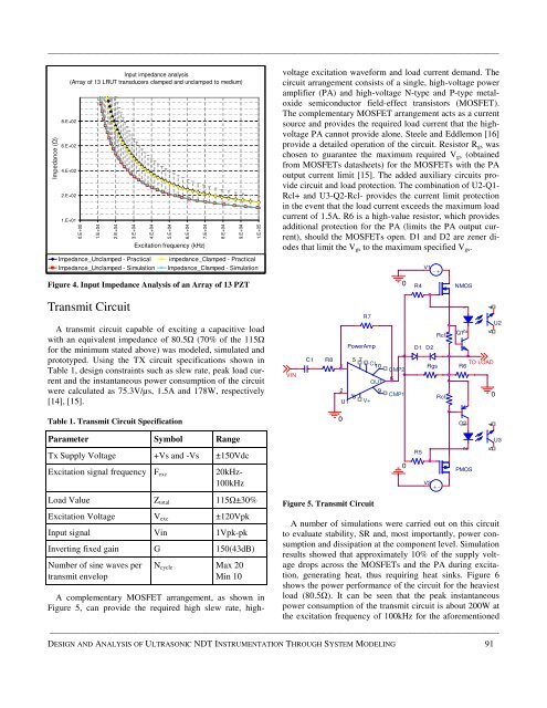
Input impedance analysis<br />
(Array <strong>of</strong> 13 LRUT transducers clamped <strong>and</strong> unclamped to medium)<br />
8.E+02<br />
6.E+02<br />
4.E+02<br />
2.E+02<br />
1.E+01<br />
0.E+00<br />
1.E+04<br />
2.E+04<br />
3.E+04<br />
4.E+04<br />
Figure 4. Input Impedance <strong>Analysis</strong> <strong>of</strong> an Array <strong>of</strong> 13 PZT<br />
5.E+04<br />
6.E+04<br />
7.E+04<br />
Excitation frequency (kHz)<br />
Impedance_Unclamped - Practical impedance_Clamped - Practical<br />
Impedance_Unclamped - Simulation Impedance_Clamped - Simulation<br />
8.E+04<br />
9.E+04<br />
1.E+05<br />
A complementary MOSFET arrangement, as shown in<br />
Figure 5, can provide the required high slew rate, highvoltage<br />
excitation waveform <strong>and</strong> load current dem<strong>and</strong>. The<br />
circuit arrangement consists <strong>of</strong> a single, high-voltage power<br />
amplifier (PA) <strong>and</strong> high-voltage N-type <strong>and</strong> P-type metaloxide<br />
semiconductor field-effect transistors (MOSFET).<br />
The complementary MOSFET arrangement acts as a current<br />
source <strong>and</strong> provides the required load current that the highvoltage<br />
PA cannot provide alone. Steele <strong>and</strong> Eddlemon [16]<br />
provide a detailed operation <strong>of</strong> the circuit. Resistor R gs was<br />
chosen to guarantee the maximum required V gs (obtained<br />
from MOSFETs datasheets) for the MOSFETs with the PA<br />
output current limit [15]. The added auxiliary circuits provide<br />
circuit <strong>and</strong> load protection. The combination <strong>of</strong> U2-Q1-<br />
Rcl+ <strong>and</strong> U3-Q2-Rcl- provides the current limit protection<br />
in the event that the load current exceeds the maximum load<br />
current <strong>of</strong> 1.5A. R6 is a high-value resistor, which provides<br />
additional protection for the PA (limits the PA output current),<br />
should the MOSFETs open. D1 <strong>and</strong> D2 are zener diodes<br />
that limit the V gs to the maximum specified V gs .<br />
0<br />
R4<br />
V1 - +<br />
NMOS<br />
Transmit Circuit<br />
A transmit circuit capable <strong>of</strong> exciting a capacitive load<br />
with an equivalent impedance <strong>of</strong> 80.5Ω (70% <strong>of</strong> the 115Ω<br />
for the minimum stated above) was modeled, simulated <strong>and</strong><br />
prototyped. Using the TX circuit specifications shown in<br />
Table 1, design constraints such as slew rate, peak load current<br />
<strong>and</strong> the instantaneous power consumption <strong>of</strong> the circuit<br />
were calculated as 75.3V/µs, 1.5A <strong>and</strong> 178W, respectively<br />
[14], [15].<br />
VIN<br />
C1<br />
R8<br />
R7<br />
PowerAmp<br />
5 7<br />
1<br />
V-CL<br />
10<br />
-<br />
OUT<br />
2<br />
9<br />
+<br />
8<br />
U1 V+<br />
CMP2<br />
6<br />
CMP1<br />
Rcl+<br />
D1 D2<br />
Rgs<br />
Rcl-<br />
Q1<br />
2 1<br />
5 4<br />
TO LOAD<br />
R6<br />
0<br />
U2<br />
Table 1. Transmit Circuit Specification<br />
Parameter Symbol Range<br />
Tx Supply Voltage +Vs <strong>and</strong> -Vs ±150Vdc<br />
Excitation signal frequency F exc<br />
20kHz-<br />
100kHz<br />
Load Value Z total 115Ω±30%<br />
Excitation Voltage V exc ±120Vpk<br />
Input signal Vin 1Vpk-pk<br />
Inverting fixed gain G 150(43dB)<br />
Number <strong>of</strong> sine waves per<br />
transmit envelop<br />
N cycle Max 20<br />
Min 10<br />
Figure 5. Transmit Circuit<br />
0<br />
V2 + -<br />
PMOS<br />
A number <strong>of</strong> simulations were carried out on this circuit<br />
to evaluate stability, SR <strong>and</strong>, most importantly, power consumption<br />
<strong>and</strong> dissipation at the component level. Simulation<br />
results showed that approximately 10% <strong>of</strong> the supply voltage<br />
drops across the MOSFETs <strong>and</strong> the PA during excitation,<br />
generating heat, thus requiring heat sinks. Figure 6<br />
shows the power performance <strong>of</strong> the circuit for the heaviest<br />
load (80.5Ω). It can be seen that the peak instantaneous<br />
power consumption <strong>of</strong> the transmit circuit is about 200W at<br />
the excitation frequency <strong>of</strong> 100kHz for the aforementioned<br />
——————————————————————————————————————————————————-<br />
DESIGN AND ANALYSIS OF ULTRASONIC <strong>NDT</strong> INSTRUMENTATION THROUGH SYSTEM MODELING 91<br />
0<br />
R5<br />
Q2<br />
2 1<br />
5 4<br />
U3