Design and Analysis of Ultrasonic NDT Instrumentation ... - IJME
Design and Analysis of Ultrasonic NDT Instrumentation ... - IJME
Design and Analysis of Ultrasonic NDT Instrumentation ... - IJME

Create successful ePaper yourself
Turn your PDF publications into a flip-book with our unique Google optimized e-Paper software.
——————————————————————————————————————————————–————<br />
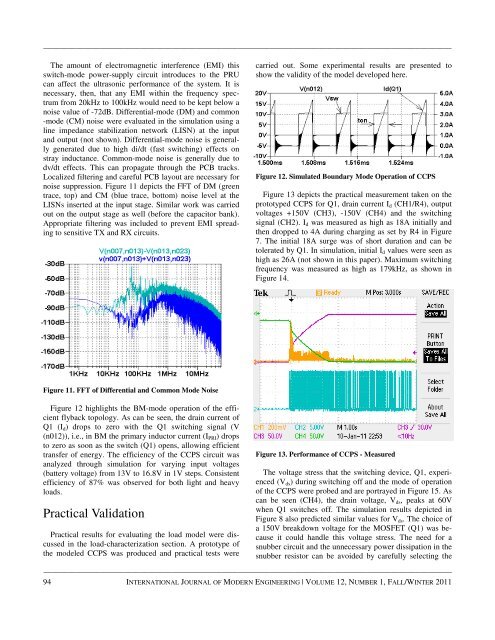
The amount <strong>of</strong> electromagnetic interference (EMI) this<br />
switch-mode power-supply circuit introduces to the PRU<br />
can affect the ultrasonic performance <strong>of</strong> the system. It is<br />
necessary, then, that any EMI within the frequency spectrum<br />
from 20kHz to 100kHz would need to be kept below a<br />
noise value <strong>of</strong> -72dB. Differential-mode (DM) <strong>and</strong> common<br />
-mode (CM) noise were evaluated in the simulation using a<br />
line impedance stabilization network (LISN) at the input<br />
<strong>and</strong> output (not shown). Differential-mode noise is generally<br />
generated due to high di/dt (fast switching) effects on<br />
stray inductance. Common-mode noise is generally due to<br />
dv/dt effects. This can propagate through the PCB tracks.<br />
Localized filtering <strong>and</strong> careful PCB layout are necessary for<br />
noise suppression. Figure 11 depicts the FFT <strong>of</strong> DM (green<br />
trace, top) <strong>and</strong> CM (blue trace, bottom) noise level at the<br />
LISNs inserted at the input stage. Similar work was carried<br />
out on the output stage as well (before the capacitor bank).<br />
Appropriate filtering was included to prevent EMI spreading<br />
to sensitive TX <strong>and</strong> RX circuits.<br />
carried out. Some experimental results are presented to<br />
show the validity <strong>of</strong> the model developed here.<br />
Figure 12. Simulated Boundary Mode Operation <strong>of</strong> CCPS<br />
Figure 13 depicts the practical measurement taken on the<br />
prototyped CCPS for Q1, drain current I d (CH1/R4), output<br />
voltages +150V (CH3), -150V (CH4) <strong>and</strong> the switching<br />
signal (CH2). I d was measured as high as 18A initially <strong>and</strong><br />
then dropped to 4A during charging as set by R4 in Figure<br />
7. The initial 18A surge was <strong>of</strong> short duration <strong>and</strong> can be<br />
tolerated by Q1. In simulation, initial I d values were seen as<br />
high as 26A (not shown in this paper). Maximum switching<br />
frequency was measured as high as 179kHz, as shown in<br />
Figure 14.<br />
Figure 11. FFT <strong>of</strong> Differential <strong>and</strong> Common Mode Noise<br />
Figure 12 highlights the BM-mode operation <strong>of</strong> the efficient<br />
flyback topology. As can be seen, the drain current <strong>of</strong><br />
Q1 (I d ) drops to zero with the Q1 switching signal (V<br />
(n012)), i.e., in BM the primary inductor current (I PRI ) drops<br />
to zero as soon as the switch (Q1) opens, allowing efficient<br />
transfer <strong>of</strong> energy. The efficiency <strong>of</strong> the CCPS circuit was<br />
analyzed through simulation for varying input voltages<br />
(battery voltage) from 13V to 16.8V in 1V steps. Consistent<br />
efficiency <strong>of</strong> 87% was observed for both light <strong>and</strong> heavy<br />
loads.<br />
Practical Validation<br />
Practical results for evaluating the load model were discussed<br />
in the load-characterization section. A prototype <strong>of</strong><br />
the modeled CCPS was produced <strong>and</strong> practical tests were<br />
Figure 13. Performance <strong>of</strong> CCPS - Measured<br />
The voltage stress that the switching device, Q1, experienced<br />
(V ds ) during switching <strong>of</strong>f <strong>and</strong> the mode <strong>of</strong> operation<br />
<strong>of</strong> the CCPS were probed <strong>and</strong> are portrayed in Figure 15. As<br />
can be seen (CH4), the drain voltage, V ds , peaks at 60V<br />
when Q1 switches <strong>of</strong>f. The simulation results depicted in<br />
Figure 8 also predicted similar values for V ds . The choice <strong>of</strong><br />
a 150V breakdown voltage for the MOSFET (Q1) was because<br />
it could h<strong>and</strong>le this voltage stress. The need for a<br />
snubber circuit <strong>and</strong> the unnecessary power dissipation in the<br />
snubber resistor can be avoided by carefully selecting the<br />
——————————————————————————————————————————————–————<br />
94 INTERNATIONAL JOURNAL OF MODERN ENGINEERING | VOLUME 12, NUMBER 1, FALL/WINTER 2011