Design and Analysis of Ultrasonic NDT Instrumentation ... - IJME
Design and Analysis of Ultrasonic NDT Instrumentation ... - IJME
Design and Analysis of Ultrasonic NDT Instrumentation ... - IJME

Create successful ePaper yourself
Turn your PDF publications into a flip-book with our unique Google optimized e-Paper software.
——————————————————————————————————————————————–————<br />
When switch Q1 is turned on, the current in the primary<br />
inductor (L 1 ) ramps up with the flux storing magnetic energy.<br />
A voltage is induced across the secondary winding (L2,<br />
L3) <strong>of</strong> a polarity such that D1 <strong>and</strong> D4 are reverse-biased.<br />
Hence, no current flows in the secondary circuit. When Q1<br />
is turned <strong>of</strong>f, the primary current drops to zero <strong>and</strong> the voltage<br />
across secondary windings L1 <strong>and</strong> L2 reverses, allowing<br />
D1 <strong>and</strong> D4 to conduct current that, in turn, charges capacitor<br />
banks C1 <strong>and</strong> C2.<br />
Flyback topology can be used in either discontinuous current<br />
mode (DCM) or continuous current mode (CCM). In<br />
general, low–voltage, high-current applications use CCM<br />
<strong>and</strong> high-voltage applications use DCM. As this is a highvoltage<br />
circuit (transmit current is only drawn from the capacitor<br />
banks), DCM is appropriate, but this method is less<br />
efficient <strong>and</strong> tends to heat up the magnetics <strong>and</strong> the switching<br />
device [17]. Boundary mode (BM) operation is also<br />
appropriate for this application. In BM, the switching current<br />
drops to zero as soon as the switch opens, which make<br />
the CCPS very efficient.<br />
There are a number <strong>of</strong> components which need to be selected<br />
before carrying out topology-specific modeling <strong>and</strong><br />
simulation <strong>of</strong> this CCPS. They were calculated <strong>and</strong> listed in<br />
Table 2 [18]. A correct selection is important in order to<br />
achieve the specified performance.<br />
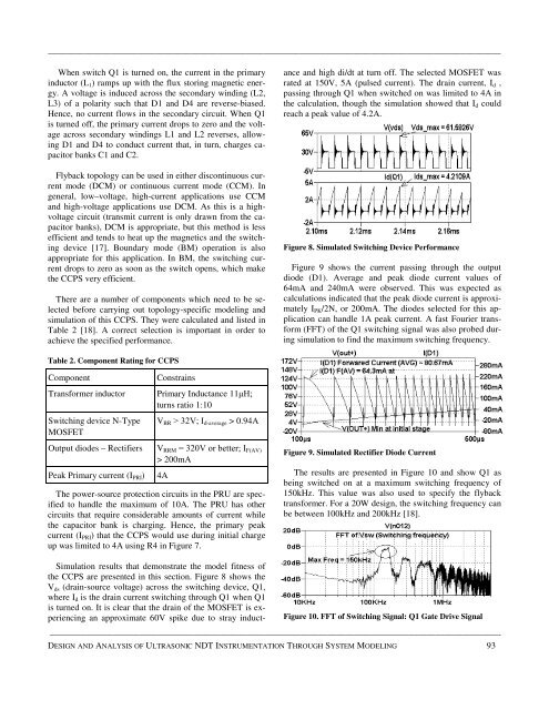
Simulation results that demonstrate the model fitness <strong>of</strong><br />
the CCPS are presented in this section. Figure 8 shows the<br />
V ds (drain-source voltage) across the switching device, Q1,<br />
where I d is the drain current switching through Q1 when Q1<br />
is turned on. It is clear that the drain <strong>of</strong> the MOSFET is experiencing<br />
an approximate 60V spike due to stray inductance<br />
<strong>and</strong> high di/dt at turn <strong>of</strong>f. The selected MOSFET was<br />
rated at 150V, 5A (pulsed current). The drain current, I d ,<br />
passing through Q1 when switched on was limited to 4A in<br />
the calculation, though the simulation showed that I d could<br />
reach a peak value <strong>of</strong> 4.2A.<br />
Figure 8. Simulated Switching Device Performance<br />
Figure 9 shows the current passing through the output<br />
diode (D1). Average <strong>and</strong> peak diode current values <strong>of</strong><br />
64mA <strong>and</strong> 240mA were observed. This was expected as<br />
calculations indicated that the peak diode current is approximately<br />
I PK /2N, or 200mA. The diodes selected for this application<br />
can h<strong>and</strong>le 1A peak current. A fast Fourier transform<br />
(FFT) <strong>of</strong> the Q1 switching signal was also probed during<br />
simulation to find the maximum switching frequency.<br />
Table 2. Component Rating for CCPS<br />
Component<br />
Transformer inductor<br />
Switching device N-Type<br />
MOSFET<br />
Output diodes – Rectifiers<br />
Peak Primary current (I PRI )<br />
Constrains<br />
Primary Inductance 11µH;<br />
turns ratio 1:10<br />
V BR > 32V; I d-average > 0.94A<br />
V RRM = 320V or better; I F(AV)<br />
> 200mA<br />
The power-source protection circuits in the PRU are specified<br />
to h<strong>and</strong>le the maximum <strong>of</strong> 10A. The PRU has other<br />
circuits that require considerable amounts <strong>of</strong> current while<br />
the capacitor bank is charging. Hence, the primary peak<br />
current (I PRI ) that the CCPS would use during initial charge<br />
up was limited to 4A using R4 in Figure 7.<br />
4A<br />
Figure 9. Simulated Rectifier Diode Current<br />
The results are presented in Figure 10 <strong>and</strong> show Q1 as<br />
being switched on at a maximum switching frequency <strong>of</strong><br />
150kHz. This value was also used to specify the flyback<br />
transformer. For a 20W design, the switching frequency can<br />
be between 100kHz <strong>and</strong> 200kHz [18].<br />
Figure 10. FFT <strong>of</strong> Switching Signal: Q1 Gate Drive Signal<br />
——————————————————————————————————————————————————-<br />
DESIGN AND ANALYSIS OF ULTRASONIC <strong>NDT</strong> INSTRUMENTATION THROUGH SYSTEM MODELING 93