Design and Analysis of Ultrasonic NDT Instrumentation ... - IJME
Design and Analysis of Ultrasonic NDT Instrumentation ... - IJME
Design and Analysis of Ultrasonic NDT Instrumentation ... - IJME

Create successful ePaper yourself
Turn your PDF publications into a flip-book with our unique Google optimized e-Paper software.
——————————————————————————————————————————————–————<br />
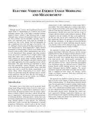
load characteristics. High current <strong>and</strong> voltage spikes at the<br />
rising edge <strong>of</strong> the waveforms are due to the short-circuit<br />
behavior <strong>of</strong> the capacitive load at the initial stage (before<br />
charging). The quiescent current <strong>of</strong> the PA was about 10mA<br />
[15]; for the applied potential <strong>of</strong> 300V pk-pk , the quiescent<br />
power consumption <strong>of</strong> the circuit was about 3W. This is<br />
also noticeable in Figure 6. The simulation results for power<br />
consumption were higher than the calculated value (177W)<br />
as the calculation steps did not account for power consumption<br />
<strong>and</strong> losses in the auxiliary components. The results presented<br />
in Figure 6 also show that the load current was 1.5A<br />
at a frequency <strong>of</strong> 100kHz.<br />
Power Consumption (W)<br />
1000<br />
100<br />
10<br />
1<br />
0.00E+00<br />
Transmit Circuit Performance<br />
Power consumption <strong>and</strong> Load current at 100kHz<br />
2.00E-05<br />
4.00E-05<br />
6.00E-05<br />
Excitation frequency (kHz)<br />
8.00E-05<br />
1.00E-04<br />
1.5<br />
1.0<br />
0.5<br />
0.0<br />
-0.5<br />
-1.0<br />
-1.5<br />
Load current (A)<br />
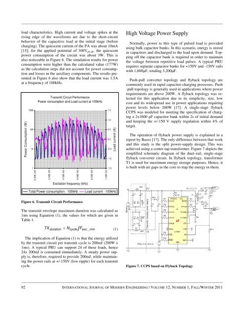
High Voltage Power Supply<br />
Normally, power to this type <strong>of</strong> pulsed load is provided<br />
using bulk capacitor banks. In this scenario, energy is stored<br />
in capacitors <strong>and</strong> discharged to the load upon dem<strong>and</strong>. Topping<br />
<strong>of</strong>f the capacitor bank is required in order to maintain<br />
the voltage between repetitive load pulses. A typical PRU<br />
requires separate capacitor banks for +150V <strong>and</strong> -150V rails<br />
with 1,600µF, totaling 3,200µF.<br />
Push-pull converter topology <strong>and</strong> flyback topology are<br />
commonly used in rapid capacitor-charging processes. Push<br />
-pull topology is generally used in applications where power<br />
requirements are above 200W. A flyback topology was selected<br />
for this application due to its simplicity, size, low<br />
cost <strong>and</strong> its widespread use in power applications requiring<br />
power levels below 200W [17]. A single-stage flyback<br />
CCPS was modeled for meeting the specification <strong>of</strong> charging<br />
a 2x1600 µF capacitor bank within 2s <strong>of</strong> initial dem<strong>and</strong><br />
<strong>and</strong> keeping the +/-150 V supply regulation within 4% <strong>of</strong><br />
target.<br />
The operation <strong>of</strong> flyback power supply is explained in a<br />
report by Basso [17]. The only difference between that work<br />
<strong>and</strong> this study is the split power-supply design. This was<br />
achieved using a center-tap transformer. Figure 7 depicts the<br />
simplified schematic diagram <strong>of</strong> the dual–rail, single-stage<br />
flyback converter circuit. In flyback topology, transformer<br />
T1 is used for maximum energy storage purposes. Hence, it<br />
is built with air gaps in the core to trap the energy in them.<br />
Total Power consumption - 100kHz<br />
Load current - 100kHz<br />
Figure 6. Transmit Circuit Performance<br />
The transmit envelope maximum duration was calculated as<br />
1ms using Equation (1), the values for which are given in<br />
Table 1.<br />
TX = N<br />
duration<br />
cycle<br />
F<br />
exc _min<br />
(1)<br />
The implication <strong>of</strong> Equation (1) is that the energy utilized<br />
by the transmit circuit per transmit cycle is 200mJ (200W x<br />
1ms). A typical PRU can support 24 <strong>of</strong> these loads, hence<br />
24x 200mJ is consumed immediately. A steady power supply<br />
is, therefore, required to provide 200mJ, while maintaining<br />
the power rails at +/-150V (low ripple) for each transmit<br />
cycle.<br />
Figure 7. CCPS based on Flyback Topology<br />
——————————————————————————————————————————————–————<br />
92 INTERNATIONAL JOURNAL OF MODERN ENGINEERING | VOLUME 12, NUMBER 1, FALL/WINTER 2011