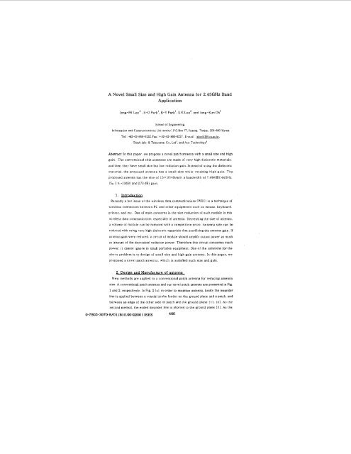
A novel small size and high gain antenna for 2.45GHz band ...
A novel small size and high gain antenna for 2.45GHz band ...
A novel small size and high gain antenna for 2.45GHz band ...

Create successful ePaper yourself
Turn your PDF publications into a flip-book with our unique Google optimized e-Paper software.
A Novel Small Size <strong>and</strong> High Gain Antenna <strong>for</strong> <strong>2.45GHz</strong> B<strong>and</strong><br />
Application<br />
Jong-Pi1 Lee''. S-0 Park', K-Y Park', S.K.Lee2. <strong>and</strong> Jung-Kun Oh3<br />
School of Engineering.<br />
In<strong>for</strong>mation <strong>and</strong> Communications University'. P 0 Box 77, Yusong, Taeion, 305-603 Korea<br />
Tel : 182-42-866-6132, Fax : + 82-12-866-5227, E-mail Iplre93@icn.ac kr,<br />
ShinA info & Telecomm Co., Ltd'. <strong>and</strong> Ace Technolog?<br />
Abstract: In this paper. we propose a <strong>novel</strong> patch <strong>antenna</strong> with a <strong>small</strong> <strong>size</strong> <strong>and</strong> <strong>high</strong><br />
<strong>gain</strong>. The conventional chip <strong>antenna</strong>s are made of very <strong>high</strong> dielectric materials,<br />
<strong>and</strong> then they have <strong>small</strong> <strong>size</strong> but low radiation <strong>gain</strong>. Instead of using the dielectric<br />
material. the proposed <strong>antenna</strong> has a <strong>small</strong> <strong>size</strong> while retaining <strong>high</strong> <strong>gain</strong>. The<br />
proposed <strong>antenna</strong> has the <strong>size</strong> of 15xl0xMmm). a b<strong>and</strong>width of 7.4%(@2.44GHz.<br />
ISii I i -10dB) <strong>and</strong> 2.73 dBi <strong>gain</strong>.<br />
1. Introduction<br />
Recently a hot issue 01 the wireless data communications (WDC) is a technique ol<br />
wireless connection between PC <strong>and</strong> other equipments such as mouse. keyboard.<br />
printer. <strong>and</strong> etc.. One 01 main concerns is the <strong>size</strong> reduction of each module in this<br />
wireless data communication. especially of <strong>antenna</strong>. Decreasing the <strong>size</strong> 01 <strong>antenna</strong>,<br />
a volume of module can be reduced with a competitive price. Antenna <strong>size</strong> can be<br />
reduced with using very <strong>high</strong> dielectric materials that sacrificing the <strong>antenna</strong> <strong>gain</strong>. If<br />
<strong>antenna</strong> <strong>gain</strong> were reduced. a circuit of module should amplify output power as mush<br />
as amount of the decreased radiation power. There<strong>for</strong>e this circuit consumes much<br />
power. it cannot ignore in <strong>small</strong> portable equipment. One of the solutions <strong>for</strong> the<br />
above problem is to design of <strong>small</strong> <strong>size</strong> <strong>and</strong> <strong>high</strong> <strong>gain</strong> <strong>antenna</strong>. In this paper, we<br />
proposed a <strong>novel</strong> patch <strong>antenna</strong>, which is satisfied such <strong>size</strong> <strong>and</strong> <strong>gain</strong><br />
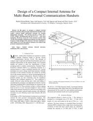
2. Design <strong>and</strong> Manufacture of <strong>antenna</strong><br />
New methods are applied to a conventional patch <strong>antenna</strong> <strong>for</strong> reducing <strong>antenna</strong><br />
<strong>size</strong>. A conventional patch <strong>antenna</strong> <strong>and</strong> our <strong>novel</strong> patch <strong>antenna</strong> are presented in Fig.<br />
1 <strong>and</strong> 2. respectively. In Fig. 2 (a). in order to minimize <strong>antenna</strong>. firstly the me<strong>and</strong>er<br />
line is applied between a coaxial probe feeder on the ground plane <strong>and</strong> a patch. <strong>and</strong><br />
between an edge of the other side of patch <strong>and</strong> the ground plane [ll, [21. As the<br />
second method. the ended me<strong>and</strong>er line IS shorted to the ground plane [31. As the<br />
o-m03-707o-a/oi /$io.oo 02001 IEEE 466
third method. both skirts (length 53 are added to both edges of patch into downward.<br />
A5 the fourth method, the patch has the offset slot (length r) at the connection part<br />
(betbeen me<strong>and</strong>er line <strong>and</strong> patch1 with maintaining the same width of me<strong>and</strong>er line<br />
The abovementioned methods have an effect on dropping the resonant frequency of<br />
<strong>antenna</strong> Since <strong>antenna</strong> material 1s just a copperplate. the proposed has an advantage<br />
or IOW COS!<br />
3. Experimental results<br />
The experimental results include the return loss (RLI. radiation pattern. <strong>and</strong><br />
<strong>antenna</strong> gam An HP8722D network analyzer <strong>and</strong> an HP5510C <strong>antenna</strong> measurement<br />
system are used <strong>for</strong> the measurement. Fig. 3 (a) shows the measured RL a<strong>gain</strong>st<br />
frequency <strong>for</strong> a conventional <strong>and</strong> proposed <strong>antenna</strong> at the same <strong>size</strong> (15xIOx6mm).<br />
The measured <strong>and</strong> computed results (using HFSS Ansoft) of the RL <strong>for</strong> the abovementioned<br />
<strong>antenna</strong> are shown in Fig 3 (al. Fig. 3 (bl <strong>and</strong> (c) show the measured<br />
results that vary with parameter S (skirt's length) <strong>and</strong> T (slot's length) In that case.<br />
all other parameters are fixed (folloumg L = 15. H= 10. W = 0.9. B = 6. G = 0.5 unit'<br />
mm) It can be seen that the resonant frequency decreases nith increasing S or T<br />
parameters. The measured <strong>and</strong> simulated results of the xy <strong>and</strong> xz-plane radiation<br />
partern are shoun in Fig. 4 that is the proposed 41h <strong>antenna</strong> model at 2.44GHz. There<br />
IS 3 good agreement wirh each other The resonant frequency of this <strong>antenna</strong> can be<br />
reduced by 50 B when compared with the conventional patch <strong>antenna</strong> (Fig. 11 The<br />
proposed <strong>antenna</strong> has useful application tor the ISM-B<strong>and</strong> (2.4-2 4835 GHd.<br />
4. Conclusions<br />
The proposed <strong>antenna</strong> has a <strong>small</strong> <strong>size</strong> <strong>and</strong> <strong>high</strong> <strong>gain</strong> that was verified with<br />
measurement <strong>and</strong> simulation. According to Fig. 3 (a). the resonant frequency of our<br />
model can be reduced by 50 % compared to the conventional patch. And resonant<br />
frequency can be controlled with varying skirt <strong>and</strong> slot's length without increasing<br />
the length height. <strong>and</strong> width of <strong>antenna</strong> The measured <strong>antenna</strong> <strong>gain</strong> has 2.73 dBi. as<br />
seen in Fig 4. Although the <strong>size</strong> of proposed <strong>antenna</strong> IS similar to that of chip<br />
<strong>antenna</strong> a <strong>gain</strong> of <strong>antenna</strong> is <strong>high</strong>er than that of chip <strong>antenna</strong> 141.<br />
References<br />
I1 1 41 Ali. <strong>and</strong> S. S. Stuchly, "A Me<strong>and</strong>er -Line Bow -Tie Antenna". Antennas <strong>and</strong><br />
Propagation Society In[. Symp.. 1996. Vo1.3. pp: 1566-1569.<br />
LEI 41. All. S. S. Stuchly. <strong>and</strong> K Caputa. .'A Wideb<strong>and</strong> Dual Me<strong>and</strong>er Sleeve Antenna"<br />
.4ntennas <strong>and</strong> Propagation Society Int. Symp.. 1996. Vol.3. pp 1598-1601.<br />
[31 R Chair. K.M. Luk. <strong>and</strong> K.F Lee. "Miniature Multilayer Shorted Patch Antenna':<br />
Electron. Lett. 2000. VoI.36. PP. 3-4.<br />
467
[41 Yuiiro Dakeya. Tsuyosi Suesada. Kenii Asakura. Norio Nakaiima <strong>and</strong> Haruhumi<br />
M<strong>and</strong>ai. “Chip Multilayer Antenna lor <strong>2.45GHz</strong>-B<strong>and</strong> Application Using LTCC<br />
Technology”, IEEE MTT-S International. 2MM Vo1.3. pp: 1693 -1696.<br />
Figure 1. Conventional patch <strong>antenna</strong><br />
(b)<br />
(C)<br />
Figure 2. The proposed model (a! unlolded (b! lolded (c) photograph<br />
468
(C)<br />
Figure 3. (a) RL of experiment <strong>and</strong> computation (b) experimental RL <strong>for</strong> different S<br />
(c) measured RL ior different T<br />
(a)<br />
(b)<br />
Figure 4. Radiation pattern<br />
(a) xy-plane (at e=90) (b) xz-plane (at @ =O)<br />
(computed: dotted. experimental: solid)<br />
469