SYSTEMS ELECTRONICS GROUP SYSTEMS ... - Sea-Seg.com
SYSTEMS ELECTRONICS GROUP SYSTEMS ... - Sea-Seg.com
SYSTEMS ELECTRONICS GROUP SYSTEMS ... - Sea-Seg.com

You also want an ePaper? Increase the reach of your titles
YUMPU automatically turns print PDFs into web optimized ePapers that Google loves.
<strong>SYSTEMS</strong> <strong>ELECTRONICS</strong> <strong>GROUP</strong><br />
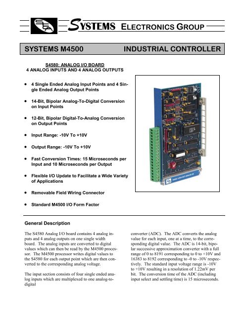
<strong>SYSTEMS</strong> M4500<br />
INDUSTRIAL CONTROLLER<br />
S4580: ANALOG I/O BOARD<br />
4 ANALOG INPUTS AND 4 ANALOG OUTPUTS<br />
• 4 Single Ended Analog Input Points and 4 Single<br />
Ended Analog Output Points<br />
• 14-Bit, Bipolar Analog-To-Digital Conversion<br />
on Input Points<br />
• 12-Bit, Bipolar Digital-To-Analog Conversion<br />
on Output Points<br />
• Input Range: -10V To +10V<br />
• Output Range: -10V To +10V<br />
• Fast Conversion Times: 15 Microseconds per<br />
Input and 10 Microseconds per Output<br />
• Flexible I/O Update to Facilitate a Wide Variety<br />
of Applications<br />
• Removable Field Wiring Connector<br />
• Standard M4500 I/O Form Factor<br />
General Description<br />
The S4580 Analog I/O board contains 4 analog inputs<br />
and 4 analog outputs on one single width<br />
board. The analog inputs are converted to digital<br />
values which can then be read by the M4500 processor.<br />
The M4500 processor writes digital values to<br />
the S4580 for each output point which are then converted<br />
to the corresponding analog voltage.<br />
The input section consists of four single ended analog<br />
inputs which are multiplexed to one analog-todigital<br />
converter (ADC). The ADC converts the analog<br />
value for each input, one at a time, to the corresponding<br />
digital value. The ADC is 14-bit, bipolar<br />
successive approximation converter with a full<br />
range of 0 to 8191 corresponding to 0 to +10V and<br />
16383 to 8192 corresponding to -0 to -10V respectively.<br />
The standard input voltage range is -10V<br />
to +10V resulting in a resolution of 1.22mV per<br />
bit. The conversion time of the ADC (including<br />
input select and settling time) is 15 microseconds.
General Description (cont’d)<br />
The output section consists of four single ended<br />
analog outputs, each equipped with it’s own digital-to-analog<br />
converter (DAC). Each DAC converts<br />
the corresponding digital value for the output<br />
to an analog voltage representing the digital value.<br />
The DACs are 12-bit, bipolar digital-to-analog<br />
converters with a full range of 800H to fffH corresponding<br />
to 0 to +10V and 0H to 7ffH corresponding<br />
to -10V to -0V respectively. The standard<br />
output voltage range is -10V to +10V resulting<br />
in a resolution of 4.88mV per bit. The conversion<br />
time of the DACs is 10 microseconds.<br />
Power for the analog section (+/-12V) is supplied via<br />
the backplane on M4510, M4512, and M4513 chassis.<br />
For all other M4500 modules/chassis, +/-12V power<br />
must be supplied via the removable field wiring connector.<br />
Refer to figure 2 for typical I/O field wiring<br />
connections and +/-12V power wiring.<br />
Program Interface<br />
As with other M4500 I/O boards, the I/O update<br />
of the S4580 is not done automatically by the<br />
M4500 processor. This provides maximum flexibility<br />
for I/O update by allowing the user to implement<br />
the I/O update as necessary (in the main program,<br />
timed interrupt, or input interrupt, etc. as<br />
required by the application). The S4580 I/O update<br />
is more <strong>com</strong>plicated than standard I/O update<br />
since the user is now directly interfacing with the<br />
ADC and DACs and thus has to perform functions<br />
such as selecting the desired analog input, initiate<br />
the conversion, wait for the conversion, read the<br />
input data, etc..<br />
The S4580 contains a “Device Select” register<br />
which is used to select the device (ADC, DAC,<br />
Analog select, etc.) that will be accessed. This<br />
register must always be set prior to accessing the<br />
desired device, otherwise erroneous results will<br />
occur. The “Device Select” register is write only<br />
and is written by setting PORT2.7 to a “1” and<br />
then writing the select <strong>com</strong>mand to byte 0 of the<br />
S4580 slot address.<br />
The following <strong>com</strong>mand codes select the respective devices<br />
on the S4580:<br />
Command Code<br />
00H<br />
01H<br />
02H<br />
03H<br />
04H<br />
Device Selected<br />
Analog Input Select<br />
ADC Select<br />
Conversion Initiate<br />
DAC0/1 Select<br />
DAC2/3 Select<br />
In addition to the above device select codes, the control<br />
bit PORT2.7 is used to select either the “Device Select”<br />
register or to actually access the respective device<br />
specified in the “Device Select” register. When<br />
PORT2.7 is “1”, the “Device Select” register is accessed.<br />
When PORT2.7 is “0”, the respective device<br />
specified in the “Device Select” register is accessed.<br />
Refer to the following example program for details on<br />
reading the analog inputs and writing the analog outputs.<br />
Program Example<br />
The following is an example of both reading analog inputs and writing analog outputs. This program uses two<br />
user functions: ufunc02() to read a specified analog input and ufunc04() to write all the analog outputs. These<br />
two user functions are called from the main program, thus the analog I/O update would occur in the main program<br />
scan.<br />
<strong>SYSTEMS</strong> Electronics Group, Arvada, CO - (303) 421-0484 - FAX (303) 421-8108 www.sea-seg.<strong>com</strong><br />
2
Main Program:<br />
******************************************************************************************************************************<br />
block: 1 - High level<br />
W104 = 7424; /* S4520 slot address (S4580 located in slot 0-0 */<br />
B102 = 0; /* Analog Input to read */<br />
ufunc02(); /* read Analog Input0 */<br />
B102 = 1; /* Analog Input to read */<br />
ufunc02(); /* read Analog Input 1 */<br />
ufunc04(); /* write all Analog Outputs */<br />
User function 2:<br />
******************************************************************************************************************************<br />
block: 1 - Assembly<br />
; This user function reads one analog input as selected by “ASEL”. Prior to calling this user function,<br />
; “ASEL” must be loaded with the analog input to be read (either 0,1,2, or 3) and “BADDR” must be<br />
; loaded with the byte 0 slot address the S4580 is in (i.e. 7424 for slot 0-0, 7488 for slot 0-1, etc.).<br />
; The user function will return with the analog value in “AIN” (W100) [0-8191 corresponds to 0 to +10V,<br />
; 16383-8192 corresponds to -0 to -10V respectively].<br />
.equ<br />
.equ<br />
.equ<br />
.equ<br />
.equ<br />
AINL,B100<br />
AINH,B101<br />
ASEL,B102<br />
ADVCE,B103<br />
BADDR,W104<br />
; select Analog Input<br />
orb PORT2,#80h ;set “Device Select”<br />
ldb ADVCE,ZERO_REG ;select “AIN Select”<br />
stb ADVCE,[BADDR] ;write to “Device Select” register on S4580<br />
andb PORT2,#7fh ;reset “Device Select”<br />
stb ASEL,[BADDR] ;select Analog Input to read<br />
; initiate ADC Conversion<br />
orb PORT2,#80h ;set “Device Select”<br />
ldb ADVCE,#02h ;select “Conversion Initiate”<br />
stb ADVCE,[BADDR] ;write to “Device Select” register on S4580<br />
andb PORT2,#7fh ;reset “Device select”<br />
stb ADVCE,[BADDR] ;start ADC conversion<br />
; read ADC<br />
orb PORT2,#80h ;set “Device Select”<br />
ldb ADVCE,#01h ;select ADC<br />
stb ADVCE,[BADDR] ;write to “Device Select” register on S4580<br />
andb PORT2,#7fh ;reset “Device Select”<br />
ld R0,BADDR ;pointer to ADC low byte<br />
ld R1,BADDR ;pointer to ADC high byte<br />
inc R1<br />
ldb R2,#02h ;wait for conversion to <strong>com</strong>plete<br />
AdcWait: djnz R2,AdcWait<br />
ldb AINL,[R0] ;read ADC low byte<br />
ldb AINH,[R1] ;read ADC high byte<br />
; B100 ( AINL ) Analog Input (low)<br />
; B101 ( AINH ) Analog Input (High)<br />
; B102 ( ASEL ) Select Analog Input<br />
; B103 (ADVCE) Analog Device Select<br />
; W104 (BADDR) S4580 Slot Address<br />
<strong>SYSTEMS</strong> Electronics Group, Arvada, CO - (303) 421-0484 - FAX (303) 421-8108 www.sea-seg.<strong>com</strong><br />
3
User function 4:<br />
********************************************************************************************************************************<br />
block: 1 - Assembly<br />
; This user function writes all analog output values to the S4580. Prior to calling this user function,<br />
; “BADDR” must be loaded with the byte 0 slot address the S4580 is in (i.e. 7424 for slot 0-0, 7488 for<br />
; slot 0-1, etc.). The values loaded into the AOUT0 thru AOUT3 analog output image registers must be<br />
; in the range of 0 to fffH where 0 corresponds to -10V out, 800H corresponds to 0V out, and fffH corresponds<br />
; to +10V out.<br />
;<br />
.equ ADVCE, B103<br />
.equ BADDR,W104<br />
.equ AOUT0,W120<br />
.equ AOUT1,W122<br />
.equ AOUT2,W124<br />
.equ AOUT3,W126<br />
; write AOUT0 and AOUT1 data<br />
orb PORT2,#80h ;set “Device Select”<br />
ldb ADVCE,#04h ;select “DAC0/1”<br />
stb ADVCE,[BADDR] ;write to “Device Select” register on S4580<br />
andb PORT2,#7fh ;reset “Device Select”<br />
ld R0,BADDR ;temporary pointer to S4580<br />
stb AOUT0,[R0]+ ;write AOUT0L to DAC0<br />
stb AOUT0+1,[R0]+ ;write AOUT0H to DAC0<br />
stb AOUT1,[R0]+ ;write AOUT1L to DAC1<br />
stb AOUT1+1,[R0] ;write AOUT1H to DAC1<br />
; write AOUT2 and AOUT3 data<br />
orb PORT2,#80h ;set “Device Select”<br />
ldb ADVCE,#05h ;select “DAC2/3”<br />
stb ADVCE,[BADDR] ;write to “Device Select” register on S4560<br />
andb PORT2,#7fh ;reset “Device Select”<br />
ld R0,BADDR ;temporary pointer to S4580<br />
stb AOUT2,[R0]+ ;write AOUT2L to DAC2<br />
stb AOUT2+1,[R0]+ ;write AOUT2H to DAC2<br />
stb AOUT3,[R0]+ ;write AOUT3L to DAC3<br />
stb AOUT3+1,[R0] ;write AOUT3H to DAC3<br />
; load (update) DACs<br />
orb PORT2,#80h ;set “Device Select”<br />
ldb ADVCE,#02h ;select “Conversion Start”<br />
stb ADVCE,[BADDR] ;write to “Device Select” on S4580<br />
andb PORT2,#7fh ;reset “Device Select”<br />
ld R0,BADDR ;point to “Load DAC” register on S4580<br />
inc R0<br />
stb ADVCE,[R0] ;update analog outputs (Load DACs)<br />
; B103 (ADVCE) Analog Device Select<br />
; W104 (BADDR) S4520 Slot Address<br />
; W120 (AOUT0) Analog Output0 value<br />
; W122 (AOUT1) Analog Output1 value<br />
; W124 (AOUT2) Analog Output2 value<br />
; W126 (AOUT3) Analog Output3 value<br />
<strong>SYSTEMS</strong> Electronics Group, Arvada, CO - (303) 421-0484 - FAX (303) 421-8108 www.sea-seg.<strong>com</strong><br />
4
Installation<br />
Prior to installing the S4580, the I/O slot addressing<br />
dip switch on the board must be set for the slot the<br />
board will be addressed as.<br />
Note: Geographical addressing is not used in the<br />
M4500. The slot the S4580 is addressed as is solely<br />
defined by the dip switch settings on the S4580 itself<br />
not by the slot in the M4500 chassis that the board is<br />
placed in. Two poles on the dip switch of the board<br />
set the binary slot address of the board as follows:<br />
S4580 SW1 Dip Switch Slot Addressing<br />
2 1 Slot Address<br />
off off 0<br />
off on 1<br />
on off 2<br />
on on 3<br />
The SW1 Slot address dip switch is located in the<br />
upper left hand corner of the <strong>com</strong>ponent side of the<br />
S4580. The respective switch pole is "on" when in<br />
either the "on" or "close" position and "off" when<br />
either in the "off" or "open" position depending on<br />
the type of dip switch used.<br />
To install the S4580 in the M4500 chassis, turn<br />
power to the M4500 "off" and remove the cover<br />
plate of the M4500 by loosening the captive screws<br />
that retain it. Install the S4580 in the respective slot<br />
of the M4500, making sure the DIN connector on<br />
the S4580 fully mates with the DIN connector in the<br />
M4500 motherboard and that the top of the S4580 is<br />
seated correctly in the card guides at the top of the<br />
M4500. Install the M4500 cover back onto the<br />
M4500 making sure the field wiring connector protrudes<br />
through the respective opening in the cover.<br />
The M4500 cover will retain the S4580 both from<br />
the top and the front, holding the S4580 in place<br />
during normal operation. Tighten the captive screws<br />
that retain the cover on the M4500. Install the female<br />
field wiring connector to the corresponding<br />
male connector on the S4580. The S4580 is now installed<br />
and ready to run. To remove the S4580, simply<br />
perform the previous steps in reverse.<br />
Specifications<br />
Board Size:<br />
Length: 6.50”<br />
Height: 4.25”<br />
Width: 0.80”<br />
Power Requirements (P4500):<br />
+5VDC:<br />
+12VDC:<br />
-12VDC:<br />
Temperature Ranges:<br />
Storage:<br />
Operating:<br />
100 milliamps<br />
50 milliamps<br />
50 milliamps<br />
0 to 85 degrees C<br />
0 to 60 degrees C<br />
Relative Humidity: 5 to 95%<br />
Input Section:<br />
Number of Analog Inputs: 4<br />
Input Range: -10V to +10V<br />
DC Input Resistance:<br />
1M ohms or greater<br />
Maximum Input Voltage: -30V to +30V<br />
Accuracy: 0.5%<br />
Repeatability: 0.1%<br />
Analog-to-Digital Conversion Method:<br />
Analog-to-Digital Conversion Time:<br />
Resolution:<br />
Successive Approximation<br />
15 microseconds<br />
14-bit<br />
<strong>SYSTEMS</strong> Electronics Group, Arvada, CO - (303) 421-0484 - FAX (303) 421-8108 www.sea-seg.<strong>com</strong><br />
5
Specifications (cont’d)<br />
Output Section:<br />
Number of Analog Outputs: 4<br />
Output Range: -10V to +10V<br />
Load Resistance:<br />
2K ohms or greater<br />
Accuracy: 0.5%<br />
Repeatability: 0.75%<br />
Digital-to-Analog Conversion time:<br />
Resolution:<br />
Short Circuit Duration:<br />
10 microseconds<br />
12-bit<br />
continuous<br />
Figure 1<br />
Typical User Wiring<br />
Figure 2<br />
Board Outline<br />
<strong>SYSTEMS</strong> Electronics Group, Arvada, CO - (303) 421-0484 - FAX (303) 421-8108 www.sea-seg.<strong>com</strong><br />
6