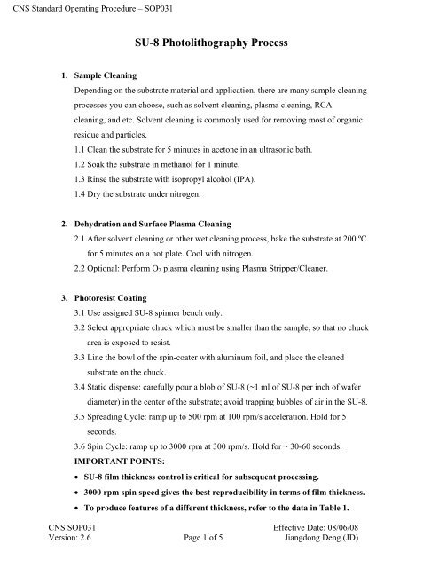
SU-8 Photolithography Process
SU-8 Photolithography Process
SU-8 Photolithography Process

Create successful ePaper yourself
Turn your PDF publications into a flip-book with our unique Google optimized e-Paper software.
CNS Standard Operating Procedure – SOP031<br />
<strong>SU</strong>-8 <strong>Photolithography</strong> <strong>Process</strong><br />
1. Sample Cleaning<br />
Depending on the substrate material and application, there are many sample cleaning<br />
processes you can choose, such as solvent cleaning, plasma cleaning, RCA<br />
cleaning, and etc. Solvent cleaning is commonly used for removing most of organic<br />
residue and particles.<br />
1.1 Clean the substrate for 5 minutes in acetone in an ultrasonic bath.<br />
1.2 Soak the substrate in methanol for 1 minute.<br />
1.3 Rinse the substrate with isopropyl alcohol (IPA).<br />
1.4 Dry the substrate under nitrogen.<br />
2. Dehydration and Surface Plasma Cleaning<br />
2.1 After solvent cleaning or other wet cleaning process, bake the substrate at 200 ºC<br />
for 5 minutes on a hot plate. Cool with nitrogen.<br />
2.2 Optional: Perform O 2 plasma cleaning using Plasma Stripper/Cleaner.<br />
3. Photoresist Coating<br />
3.1 Use assigned <strong>SU</strong>-8 spinner bench only.<br />
3.2 Select appropriate chuck which must be smaller than the sample, so that no chuck<br />
area is exposed to resist.<br />
3.3 Line the bowl of the spin-coater with aluminum foil, and place the cleaned<br />
substrate on the chuck.<br />
3.4 Static dispense: carefully pour a blob of <strong>SU</strong>-8 (~1 ml of <strong>SU</strong>-8 per inch of wafer<br />
diameter) in the center of the substrate; avoid trapping bubbles of air in the <strong>SU</strong>-8.<br />
3.5 Spreading Cycle: ramp up to 500 rpm at 100 rpm/s acceleration. Hold for 5<br />
seconds.<br />
3.6 Spin Cycle: ramp up to 3000 rpm at 300 rpm/s. Hold for ~ 30-60 seconds.<br />
IMPORTANT POINTS:<br />
• <strong>SU</strong>-8 film thickness control is critical for subsequent processing.<br />
• 3000 rpm spin speed gives the best reproducibility in terms of film thickness.<br />
• To produce features of a different thickness, refer to the data in Table 1.<br />
CNS SOP031 Effective Date: 08/06/08<br />
Version: 2.6 Page 1 of 5 Jiangdong Deng (JD)
CNS Standard Operating Procedure – SOP031<br />
4. Soft Baking<br />
4.1 Right after photoresist coating, pre-bake the substrate at 65 °C on a hot plate. The<br />
pre-bake times for different thicknesses are shown in Table 1.<br />
4.2 Ramp the hot plate to 95 °C for soft-baking. Refer to Table 1 for the soft-bake<br />
time.<br />
4.3 After soft bake complete, turn off the hot plate and let the substrates cool slowly to<br />
room temperature.<br />
NOTES<br />
• The hot plate needs to be leveled carefully so that the layer of <strong>SU</strong>-8 is of uniform<br />
thickness.<br />
• Any air bubbles can be removed during the bake at 95 °C by gently tapping the air<br />
bubbles with a 24-gauge needle.<br />
5. Edge Bead Removal (EBR) (optional)<br />
NOTE: For thicker <strong>SU</strong>-8 (>20um) or high aspect ratio feature (height size:feaure<br />
size > 2:1) process, it is strongly recommended to remove the edge bead in order<br />
to get better contact between the photomask and the photoresist layer.<br />
5.1 Place the substrate back on the chuck of the spin coater. Ramp up to 500 rpm at<br />
100 rpm/s acceleration. Hold for 20-30 seconds.<br />
5.2 While the substrate is spinning at 500 rpm, inject about 3-5 ml of PGMEA<br />
(Propylene Glycol Monomethyl Ether Acetate) or <strong>SU</strong>-8 Developer in a steady<br />
stream through a 24-gauge needle to the outer rim of the substrate in order to<br />
dissolve the edge bead.<br />
5.3 Ramp up to 1000 rpm at 300 rpm/s. Hold for 20 seconds.<br />
5.4 Bake the substrate at 65 °C on a hot plate for 2 minutes to dry off the residual<br />
solvent (developer).<br />
CNS SOP031 Effective Date: 08/06/08<br />
Version: 2.6 Page 2 of 5 Jiangdong Deng (JD)
CNS Standard Operating Procedure – SOP031<br />
Table1. <strong>Process</strong> Conditions for <strong>SU</strong>-8 photolithography<br />
Required<br />
<strong>SU</strong>8<br />
Thickness<br />
(um)<br />
<strong>SU</strong>-8 type (*1) Sp in Prebakinbaking<br />
Soft-<br />
Exposure (*2) Suggest (*3) Suggest Post-Exp<br />
speed<br />
Energy Exposure Exposure Baking 1<br />
(rpm)/ramp-<br />
time (65C, time (95C, (mJ/cm^2) Energy time (AB- PEB1<br />
time/hold-<br />
time<br />
min) min)<br />
(mJ/cm^2)<br />
(+/-10%)<br />
M) (sec) (65C,min)<br />
Post-Exp<br />
Baking 2<br />
PEB2<br />
(95C,min)<br />
1.5 2 3000/ 8s /60s 1 1 70-100 85 3.5 1 1 1<br />
PGMEA<br />
Develop<br />
time<br />
(min)<br />
Comment<br />
(*4)<br />
Verified<br />
Thickness<br />
(um) -CR1<br />
(*5)<br />
2 2002 3000/ 8s /60s 1 2 70-100 85 3.5 1 1 1 CNS<br />
5 2005 3000/ 8s /60s 1 2 80-120 100 4.2 1 1 1<br />
5 5 3000/ 8s /60s 1 3 80--110 100 4.2 1 1 1<br />
7 2007 3000/ 8s /60s 1 2 90-140 115 4.5 1 1.5 1<br />
10 2010 3000/ 8s /60s 1 2 110-170 140 5.5 1 2.5 2 CNS<br />
10 10 3000/ 8s /60s 2 5 100-170 140 5.5 1 2.5 2<br />
15 2015 3000 / 8s /60s 1 2 120-190 160 6.5 1 2+1 3 CNS 14 (+/-0.5)<br />
20 2015 2000 / 5s /60s 1 3 140-230 190 7.4 1 2+1 3 CNS<br />
25 2025 3000 / 8s /60s 1 3 150--250 200 8 1 3+1 4 CNS 24 (+/-1)<br />
35 2035 3000 / 8s /60s 2 5 180-300 240 9.5 1 3+1 5<br />
40 50 3000 / 8s /60s 5 15 250-300 280 11 1 4+1 6 CNS<br />
50 2050 3000 / 8s /45s 3 6 230-380 310 12 1 7+1 6 CNS 56 (+/- 4)<br />
75 2075 3000 / 8s /45s 3 9 280-470 380 15 1 7+1 7<br />
100 2100 3000 / 8s /45s 5 20 320--540 430 17.5 1 10+1 10 CNS<br />
3000 rpm of spin speed is recommended for the better repeabability of film thickness<br />
Suggest exposure energy is given under follwing conditions: Plastic film pattern mask, a 360nm LP filter to hold the mask and Si substrate<br />
Suggest exposure time is based on the intensity of AB-M at 365nm ~25mW/cm^2<br />
Some of <strong>SU</strong>8 are provided by CNS, as marked in the Comment column,<br />
3 types of <strong>SU</strong>-8 (2015,2025, 2050) have been verified in LISE clean-room of CNS (<strong>SU</strong>-8 banch, rightside spinner, which are highlighted.<br />
6. Exposure<br />
6.1 Two mask aligners in CNS can be used for <strong>SU</strong>-8 exposure: AB-M mask aligner<br />
and <strong>SU</strong>SS MJB4 mask aligner.<br />
6.2 To operate the mask aligner, follow the standard operating procedure for AB-M<br />
aligner (CNS SOP017) or <strong>SU</strong>SS MJB4 (CNS SOP0XX).<br />
6.3 Set the exposure time as recommended in Table 1 and perform the exposure.<br />
Important Note for <strong>SU</strong>-8 UV Exposure:<br />
• For a film (transparency) photomask: place the photomask on top of the<br />
substrate with the printed side of the mask facing the photoresist layer on the<br />
substrate. Mount a blank glass plate on the mask holder.<br />
• Place a 360nm long-pass (LP) filter on the glass plate (or the chrome mask) to<br />
reduce the short wavelength effect and improve the feature profile. Add 20%-<br />
40% more exposure time to compensate for the intensity loss due to the filter.<br />
CNS SOP031 Effective Date: 08/06/08<br />
Version: 2.6 Page 3 of 5 Jiangdong Deng (JD)
CNS Standard Operating Procedure – SOP031<br />
7. Post Expose Bake (PEB)<br />
7.1 Place the substrate on a hot plate and post exposure bake (PEB) at 65 °C. The<br />
recommended baking times (PEB 1) are outlined in Table 1 for different <strong>SU</strong>-8<br />
thicknesses.<br />
7.2 Ramp the hot plate to 95 °C for the second step post exposure bake (PEB 2).<br />
Refer to Table 1 for the baking time for PEB 2.<br />
7.3 Let the hot plate and substrates cool slowly to room temperature.<br />
Note: Rapidly cooling the substrate may cause thermal stress built in the <strong>SU</strong>-8<br />
film, and results in film crack.<br />
8. Development<br />
8.1 Immerse the substrate in a bath of PGMEA or <strong>SU</strong>-8 Developer and gently rock the<br />
dish for agitation. Refer to Table 1 for the developing time for features of <strong>SU</strong>-8 of<br />
varying thickness.<br />
8.2 Soak the substrate in an IPA bath for ~30 seconds.<br />
Note: A whitish residue on the surface of the substrate is an indication of underdevelopment.<br />
Repeat the previous step 1-2 minutes at a time until no whitish<br />
residue is observed in the IPA bath,<br />
8.3 Dry the front and back of the substrate under a stream of N 2 .<br />
9. Pattern Characterization<br />
9.1 Observe the substrate under the microscope with the red filter in place to determine<br />
the quality of the developed features.<br />
9.2 Use the Veeco Dektak 6M profilometer to measure the height of the features.<br />
Refer to the standard operating procedure of Dektak 6M.<br />
Version History<br />
Revision Date Author Changes<br />
2.0 03/18/08 JD Initial draft<br />
2.1 05/28/08 EM Minor clerical updates.<br />
2.2 05/30/08 FK Minor changes, content additions, and comments.<br />
2.3 08/05/08 EM Merged comments from FK, LX.<br />
2.4 08/06/08 FK Minor corrections.<br />
2.5 08/07/08 JD Modify the process table 1, modify the process<br />
steps and conditions.<br />
2.6 08/18/08 LX, JD Minor changes<br />
CNS SOP031 Effective Date: 08/06/08<br />
Version: 2.6 Page 4 of 5 Jiangdong Deng (JD)
CNS Standard Operating Procedure – SOP031<br />
--------------------------- End of Document ---------------------------<br />
CNS SOP031 Effective Date: 08/06/08<br />
Version: 2.6 Page 5 of 5 Jiangdong Deng (JD)