Millenium Science Complex - Center for Nanoscale Systems
Millenium Science Complex - Center for Nanoscale Systems
Millenium Science Complex - Center for Nanoscale Systems

Create successful ePaper yourself
Turn your PDF publications into a flip-book with our unique Google optimized e-Paper software.
<strong>Millenium</strong> <strong>Science</strong> <strong>Complex</strong><br />
New clean room: 10,000 sq. ft. class 100/1000<br />
Support space : 6,500 sq. ft
Savannah_200<br />
• Al 2 O 3 (1.1Å GPC @200°C)<br />
• HfO 2 (1Å GPC @110 °C)<br />
• Ta 2 O 5<br />
• TiO 2 (0.457ÅGPC @150 o C)<br />
Titanium isopropoxide Ti(OiPr)4<br />
Tetrakis(dimethylamino)titanium (TDMAT)<br />
• ZrO 2<br />
• ZnO 2 (stopped due to cross contamination)<br />
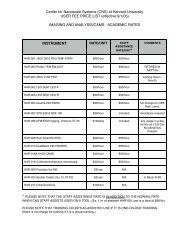
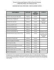
Usage:08-present<br />
• ~2,000 hrs per year ~23% based on 24/7<br />
• $50 per use <strong>for</strong> academic $100 <strong>for</strong> industry be<strong>for</strong>e 3/1/12<br />
$75 per use <strong>for</strong> academic $150 <strong>for</strong> industry after 3/1/12<br />
• $1 per 1nm<br />
• $20,000 per year
High con<strong>for</strong>mity of ALD coating<br />
Cross-sectional FESEM view of 20 nm HfO 2
Comparison between seeded and unseeded ALD<br />
deposition on graphene by AFM<br />
J. Robinson The Electro-Optics <strong>Center</strong>, Department of Materials <strong>Science</strong> and Engineering, Materials Research Institute,<br />
The Pennsylvania State University
Cross-sectional TEM characterization<br />
TiO 2<br />
graphene<br />
1.5 nm<br />
SiC<br />
TiO 2 on Ti-seeded graphene @250°C<br />
HfO 2<br />
1.5 nm<br />
graphene<br />
SiC<br />
HfO 2 on graphene @110°C<br />
X. Weng, J. Robinson The Electro-Optics <strong>Center</strong>, Department of Materials <strong>Science</strong> and Engineering, Materials Research<br />
Institute, The Pennsylvania State University
Cross-sectional TEM characterization<br />
Al 2 O 3<br />
1.5 nm<br />
graphene<br />
SiC<br />
Al 2 O 3 on Al-seeded graphene @300°C<br />
Ta 2 O 5<br />
1.5 nm<br />
defective carbon region<br />
graphene<br />
SiC<br />
Ta 2 O 5 on Ta-seeded graphene @150°C<br />
X. Weng, J. Robinson The Electro-Optics <strong>Center</strong>, Department of Materials <strong>Science</strong> and Engineering, Materials Research<br />
Institute, The Pennsylvania State University
Electrical test of Al 2 O 3 using MOSCAP<br />
Dielectric constant : ~ 8<br />
k=7.75<br />
k=8.37<br />
thinnest electrical oxide<br />
thickness (EOT) achieved till<br />
date is 12 A (1.2 nm)<br />
Prof. Suman Datta’s group, Department of Electrical Engineering, Materials Research Institute The Pennsylvania State University
Si MOSCAP with alumina<br />
- Leakage<br />
I leakage<br />
[A/cm 2 ]<br />
10 1<br />
10 0 Be<strong>for</strong>e FGA Alumina on Si (25cycle)<br />
10 -1<br />
Alumina on Si (50cycle)<br />
Alumina on Si (75cycle)<br />
10 -2<br />
10 -3<br />
10 -4<br />
10 -5<br />
10 -6<br />
10 -7<br />
10 -8<br />
10 -9<br />
10 -10<br />
10 -11<br />
10 -12<br />
-2 -1 0 1 2<br />
V G<br />
[V]<br />
I leakage<br />
[A/cm 2 ]<br />
10 1<br />
10 0 After FGA<br />
10 -1<br />
(350C, 1hour)<br />
10 -2<br />
10 -3<br />
10 -4<br />
10 -5<br />
10 -6<br />
10 -7<br />
10 -8<br />
10 -9<br />
10 -10<br />
10 -11<br />
10 -12<br />
-2 -1 0 1 2<br />
V G<br />
[V]<br />
Alumina on Si (25cycles)<br />
Alumina on Si (50cycles)<br />
Alumina on Si (75cycles)<br />
Leakage improves significantly <strong>for</strong> the 1.2 nm EOT gate stack<br />
by <strong>for</strong>ming gas anneal at 350C <strong>for</strong> 1 hour<br />
Prof. Suman Datta’s group, Department of Electrical Engineering, Materials Research Institute The Pennsylvania State University
This version of CasaXPS is owned by Penn State University<br />
This version of CasaXPS is owned by Penn State University<br />
F outgassing characterization by Auger & XPS<br />
F<br />
10 sec sputtering<br />
Al<br />
F found in the<br />
top surface<br />
O<br />
C<br />
F<br />
50 nm nm Al 2 O 3 @ 300°C
This version of CasaXPS is owned by Penn State University<br />
This version of CasaXPS is owned by Penn State University<br />
F contamination depends on process temperature<br />
#1. 300 °C<br />
#2. 80 °C<br />
#1. 50 nm Al 2 O 3 @ 300°C<br />
#2. 50 nm Al 2 O 3 @ 80°C<br />
Kalrez 4079 1 month old
This version of CasaXPS is owned by Penn State University<br />
This version of CasaXPS is owned by Penn State University<br />
F contamination depends on the age of O-ring<br />
C<br />
#1. 1 viton<br />
F<br />
#2. Kalrez 4079 1 month old<br />
#3. Kalrez 4079 11 month old
Auger analysis on Al 2 O 3 sample prepared by<br />
Cambridge Nanotech<br />
F<br />
5 sec sputtering<br />
Al<br />
O<br />
40.9 nm Al 2 O 3 , 250°C Cambridge Nanotech
This version of CasaXPS is owned by Penn State University<br />
Auger analysis on SiO 2 sample prepared by<br />
Cambridge Nanotech<br />
F<br />
Al<br />
O<br />
C<br />
34.7nm SiO 2 grown at 250°C<br />
Cambridge Nanotech
This version of CasaXPS is owned by Penn State University<br />
No F found in SiO 2 sample prepared by Fiji<br />
Al<br />
O<br />
C<br />
21 nm nm Al 2 O 3 Fiji Cambridge Nanotech
Conclusions:<br />
• F contamination can be found on all films prepared on Savannah<br />
systems<br />
• The source of F comes from O-ring outgassing<br />
• All high temperature O-rings made of fluorocarbon or<br />
perfluorocarbon materials have this issue<br />
• F contamination depends on process temperature and O-ring age<br />
Question:<br />
How F contamination relates to electrical leakage<br />
Fact:<br />
All films contains F on the surface (possibly not at the interface), but<br />
not all films leaks.
F outgassing -> pitting on the lid -><br />
vacuum leaking ->electrical leakage<br />
pitting occurs outside o-ring<br />
O-ring
Vacuum maintenance<br />
Leak checking regularly<br />
• Rate of rise 20-50 mtorr/min<br />
• He leak detector<br />
Two Al lids to swap regularly ( every 2 or 3 months)<br />
Making another stainless steel lid<br />
Change O-ring regularly<br />
Kelretz 4079
O-rings:<br />
Viton<br />
204 °C cheap<br />
Kelretz 4079 316°C $457.00<br />
Kelretz 7075 327°C $457.00<br />
FFKM 75 Black Perlast 327°C $325.24<br />
(low outgassing, size G75TX,<br />
Precision Polymer Engineering Ltd., UK)
Cross contamination: ZnO<br />
Facts:<br />
User complained about degraded<br />
optical and electrical properties after<br />
ZnO deposition<br />
Solutions:<br />
Capping chamber by Al 2 O 3<br />
Complete chamber cleaning<br />
Replacing manifold<br />
Stopped doing ZnO<br />
SIMS analysis of Al 2 O 3
Major issues<br />
• Electrical leakage<br />
1. Cross contamination: ZnO<br />
2. Chamber leak -- O-ring etches Al lid(F outgassing)<br />
• Software crashes frequently due to RF noise<br />
• Self contamination<br />
1. ALD valve<br />
2. Stop valve<br />
3. Gauge- pulse dips
Major modifications<br />
1. Expanded to 6-fold manifold<br />
2. Made a second Al lid<br />
2. To replace the Al lid w/ a<br />
stainless steel lid<br />
3. To replace the existing black<br />
box w/ a silver box
Proposed dual chamber ALD tool<br />
ALD growth chamber<br />
• UHV compatible 10 -8 torr<br />
• Substrate heater up to 600°C<br />
• thermal ALD & plasma enhanced<br />
ALD<br />
• H2, N2 and O2 as plasma gas<br />
• 6 precursor gas lines<br />
Prep chamber:<br />
• UHV compatible 10 -8 torr<br />
• Substrate heating to 600 °C<br />
• O 2 , H 2 , N 2 and Ar<br />
• Effusion cell<br />
• Ion beam gun<br />
• RF atom source<br />
• e-beam evaporator<br />
• Gas injector<br />
In situ monitoring<br />
capability options<br />
• Differentially pumped<br />
RHEED system<br />
• Ellipsometry<br />
• DS/RAS optical<br />
access (normal<br />
incidence)