Nanofabrication and Optical Properties - Center for Nanoscale ...
Nanofabrication and Optical Properties - Center for Nanoscale ...
Nanofabrication and Optical Properties - Center for Nanoscale ...

You also want an ePaper? Increase the reach of your titles
YUMPU automatically turns print PDFs into web optimized ePapers that Google loves.
Silver Nanorings: <strong>Nanofabrication</strong> <strong>and</strong> <strong>Optical</strong> <strong>Properties</strong><br />
Julie Stern<br />
Physics <strong>and</strong> Chemistry, Stony Brook University<br />
NNIN REU Site: <strong>Center</strong> <strong>for</strong> Imaging <strong>and</strong> Mesoscale Structures, Harvard University<br />
NNIN REU Principal Investigator <strong>and</strong> Mentor: Prof. Ken Crozier, Division of Engineering<br />
<strong>and</strong> Applied Sciences, Harvard University<br />
Contact: jvstern@aol.com, kcrozier@deas.harvard.edu<br />
OPTICS<br />
Introduction:<br />
Metallic nanoparticles have become of interest <strong>for</strong> a wide<br />
variety of applications areas due to their optical properties.<br />
These properties include optical surface resonance, localization,<br />
confinement, enhancement of electric fields, <strong>and</strong> resonance<br />
wavelength tunability as a function of geometry. The main goal<br />
of this study is to elucidate the viability of silver nanorings<br />
in achieving these optical characteristics. Silver having less<br />
optical loss than gold is expected to achieve better results.<br />
An additional goal of this study is to achieve the resonant<br />
wavelength redshift from visible towards infrared wavelengths<br />
often observed with gold nanoshells <strong>and</strong> gold nanorings when<br />
geometrical parameters are tuned. The geometrical parameters<br />
under consideration consist of varying the inner ring radius as<br />
compared to the outer ring radius <strong>and</strong> fabricating nanorings<br />
with subwavelength dimensions. To obtain subwavelength<br />
spatial dimensions the nanofabrication process includes e-<br />
beam lithography at high resolution. Preliminary results from<br />
nanofabricating the silver nanorings <strong>and</strong> optical analysis are<br />
presented.<br />
The physical phenomena we expect to obtain from the silver<br />
nanorings involve surface plasmon resonances. In metals, the<br />
charge density undergoes periodic oscillations creating dipolar<br />
<strong>and</strong> multipolar patterns of electric charges. This in turn results<br />
in electric field enhancement in subwavelength regions near<br />
the top <strong>and</strong> bottom rims outside of the rings.<br />
It has been shown with gold nanorings [1] that the extinction<br />
peaks are in the near-infrared region with peak wavelengths<br />
affected by geometry, the ratio of the ring wall thickness to<br />
the radius of the ring. As this ratio decreased, from 0.22 to<br />
0.16 <strong>for</strong> the gold nanorings of [1], the resonant wavelength<br />
redshifts by 400 nm.<br />
The importance of metallic nanoparticles is evident in<br />
the applications they contribute to. One application area is<br />
ultra-sensitive single molecule detection [2]. Cancer therapy<br />
has been under development <strong>and</strong> consists of applying gold<br />
nanoshells to treat cancer [3]. Another application concept<br />
involves the idea that materials on their own rarely resonate<br />
at the near-infrared or infrared wavelengths [4] <strong>and</strong> that the<br />
ability to tune to these wavelengths by changing geometry<br />
opens new application possibilities.<br />
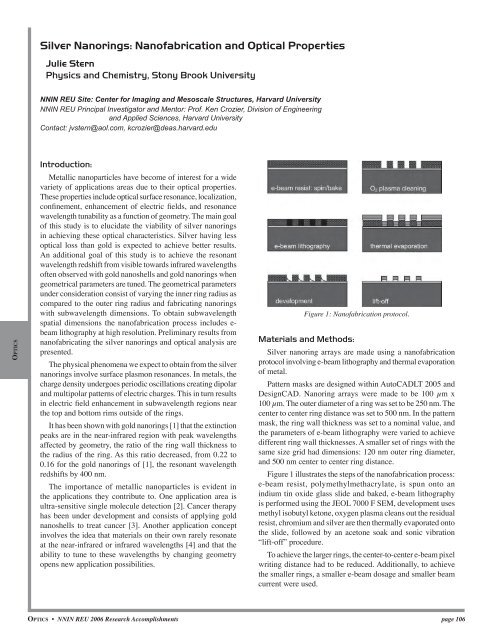
Figure 1: <strong>Nanofabrication</strong> protocol.<br />
Materials <strong>and</strong> Methods:<br />
Silver nanoring arrays are made using a nanofabrication<br />
protocol involving e-beam lithography <strong>and</strong> thermal evaporation<br />
of metal.<br />
Pattern masks are designed within AutoCADLT 2005 <strong>and</strong><br />
DesignCAD. Nanoring arrays were made to be 100 µm x<br />
100 µm. The outer diameter of a ring was set to be 250 nm. The<br />
center to center ring distance was set to 500 nm. In the pattern<br />
mask, the ring wall thickness was set to a nominal value, <strong>and</strong><br />
the parameters of e-beam lithography were varied to achieve<br />
different ring wall thicknesses. A smaller set of rings with the<br />
same size grid had dimensions: 120 nm outer ring diameter,<br />
<strong>and</strong> 500 nm center to center ring distance.<br />
Figure 1 illustrates the steps of the nanofabrication process:<br />
e-beam resist, polymethylmethacrylate, is spun onto an<br />
indium tin oxide glass slide <strong>and</strong> baked, e-beam lithography<br />
is per<strong>for</strong>med using the JEOL 7000 F SEM, development uses<br />
methyl isobutyl ketone, oxygen plasma cleans out the residual<br />
resist, chromium <strong>and</strong> silver are then thermally evaporated onto<br />
the slide, followed by an acetone soak <strong>and</strong> sonic vibration<br />
“lift-off” procedure.<br />
To achieve the larger rings, the center-to-center e-beam pixel<br />
writing distance had to be reduced. Additionally, to achieve<br />
the smaller rings, a smaller e-beam dosage <strong>and</strong> smaller beam<br />
current were used.<br />
OPTICS • NNIN REU 2006 Research Accomplishments page 106
<strong>Optical</strong> characterization demonstrated resonances in the<br />
near-infrared wavelength range. In addition, the results showed<br />
that the resonances could be tuned to different wavelengths by<br />
changing the ring thickness.<br />
Hence, the nanofabrication process worked <strong>for</strong> silver<br />
nanorings. High resolution e-beam lithography was needed<br />
to produce even smaller rings. The rings absorbed resonances<br />
within the near-infrared region of wavelengths. Geometric<br />
tunability of the optical modes was shown.<br />
Figure 2: Silver nanorings.<br />
Transmission data is measured from the fabricated nanoring<br />
array sample. Visible light from a xenon lamp irradiates the<br />
silver nanoring array head on. The light transmitted by the<br />
nanoring is collected into an optical fiber <strong>and</strong> into an optical<br />
spectrum analyzer. The data is normalized by incident light. A<br />
dip in transmission corresponds to a peak in absorption.<br />
The SEM images were taken with the Leo 982 field emission<br />
scanning electron microscope.<br />
Results <strong>and</strong> Conclusions:<br />
The resulting silver nanoring array produced from the<br />
nanofabrication procedure <strong>and</strong> SEM imaging are shown<br />
in Figure 2. For a sample ring, the outer ring diameter was<br />
measured to be roughly 386 nm with a ring wall thickness of<br />
80 nm. Figure 3 illustrates a tilted view of the same sample.<br />
Smaller rings were nanofabricated (Figure 4). Only a minute<br />
amount of ring de<strong>for</strong>mity <strong>and</strong> interior residual appeared.<br />
For a sample smaller-sized ring, the outer ring diameter was<br />
measured to be roughly 187 nm. The ring wall thickness was<br />
measured to be approximately 33.4 nm.<br />
Acknowledgements:<br />
Special thanks to my mentor, Prof. Ken Crozier, Division<br />
of Engineering <strong>and</strong> Applied Sciences, Harvard University.<br />
This work was supported by the NSF <strong>and</strong> NNIN. Thanks to<br />
Kathryn Hollar, DEAS, Harvard. Special thanks to Yuan Lu,<br />
Jiangdong Deng, Ed Macomber, Ling Xie, Steven Sheppard,<br />
<strong>and</strong> David Lange of the <strong>Center</strong> <strong>for</strong> <strong>Nanoscale</strong> Systems at<br />
Harvard University. Thanks to Emre Togan.<br />
References:<br />
[1] Aizpurua, J., Hanarp, P., Sutherl<strong>and</strong>, D. S., Käll, M., Bryant,<br />
Garnett W., García de Abajo, F. J., “<strong>Optical</strong> <strong>Properties</strong> of Gold<br />
Nanorings,” Phys. Rev. Lett. 90, 057401 (2003).<br />
[2] Alivisatos, P., “The use of nanocrystals in biological detection,”<br />
Nature Biotechnology, Vol 22, No 1, Jan (2004).<br />
[3] Loo, C., Lin, A., Hirsh, L., Lee, M., Barton, J., Halas, N., West,<br />
J., Drezek, R., “Nanoshell-Enabled Photonics-Based Imaging<br />
<strong>and</strong> Therapy of Cancer,” Technology in Cancer Research <strong>and</strong><br />
Treatment, Vol 3, Number 1, February (2001).<br />
[4] Oldenburg, S. J., Averitt, R. D., Westcott, S. L., Halas, N. J.,<br />
“Nanoengineering of optical resonances,” Chemical Physics<br />
Letters, 288, 243-247 (1998).<br />
OPTICS<br />
Figure 3: Tilted view of silver nanorings.<br />
Figure 4: Smaller silver nanorings.<br />
page 107<br />
NNIN REU 2006 Research Accomplishments • OPTICS