Nanofabrication and Optical Properties - Center for Nanoscale ...
Nanofabrication and Optical Properties - Center for Nanoscale ...
Nanofabrication and Optical Properties - Center for Nanoscale ...

You also want an ePaper? Increase the reach of your titles
YUMPU automatically turns print PDFs into web optimized ePapers that Google loves.
<strong>Optical</strong> characterization demonstrated resonances in the<br />
near-infrared wavelength range. In addition, the results showed<br />
that the resonances could be tuned to different wavelengths by<br />
changing the ring thickness.<br />
Hence, the nanofabrication process worked <strong>for</strong> silver<br />
nanorings. High resolution e-beam lithography was needed<br />
to produce even smaller rings. The rings absorbed resonances<br />
within the near-infrared region of wavelengths. Geometric<br />
tunability of the optical modes was shown.<br />
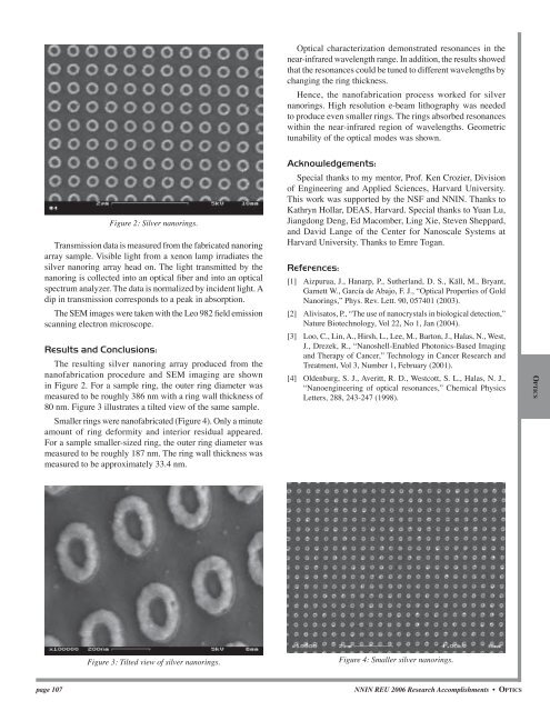
Figure 2: Silver nanorings.<br />
Transmission data is measured from the fabricated nanoring<br />
array sample. Visible light from a xenon lamp irradiates the<br />
silver nanoring array head on. The light transmitted by the<br />
nanoring is collected into an optical fiber <strong>and</strong> into an optical<br />
spectrum analyzer. The data is normalized by incident light. A<br />
dip in transmission corresponds to a peak in absorption.<br />
The SEM images were taken with the Leo 982 field emission<br />
scanning electron microscope.<br />
Results <strong>and</strong> Conclusions:<br />
The resulting silver nanoring array produced from the<br />
nanofabrication procedure <strong>and</strong> SEM imaging are shown<br />
in Figure 2. For a sample ring, the outer ring diameter was<br />
measured to be roughly 386 nm with a ring wall thickness of<br />
80 nm. Figure 3 illustrates a tilted view of the same sample.<br />
Smaller rings were nanofabricated (Figure 4). Only a minute<br />
amount of ring de<strong>for</strong>mity <strong>and</strong> interior residual appeared.<br />
For a sample smaller-sized ring, the outer ring diameter was<br />
measured to be roughly 187 nm. The ring wall thickness was<br />
measured to be approximately 33.4 nm.<br />
Acknowledgements:<br />
Special thanks to my mentor, Prof. Ken Crozier, Division<br />
of Engineering <strong>and</strong> Applied Sciences, Harvard University.<br />
This work was supported by the NSF <strong>and</strong> NNIN. Thanks to<br />
Kathryn Hollar, DEAS, Harvard. Special thanks to Yuan Lu,<br />
Jiangdong Deng, Ed Macomber, Ling Xie, Steven Sheppard,<br />
<strong>and</strong> David Lange of the <strong>Center</strong> <strong>for</strong> <strong>Nanoscale</strong> Systems at<br />
Harvard University. Thanks to Emre Togan.<br />
References:<br />
[1] Aizpurua, J., Hanarp, P., Sutherl<strong>and</strong>, D. S., Käll, M., Bryant,<br />
Garnett W., García de Abajo, F. J., “<strong>Optical</strong> <strong>Properties</strong> of Gold<br />
Nanorings,” Phys. Rev. Lett. 90, 057401 (2003).<br />
[2] Alivisatos, P., “The use of nanocrystals in biological detection,”<br />
Nature Biotechnology, Vol 22, No 1, Jan (2004).<br />
[3] Loo, C., Lin, A., Hirsh, L., Lee, M., Barton, J., Halas, N., West,<br />
J., Drezek, R., “Nanoshell-Enabled Photonics-Based Imaging<br />
<strong>and</strong> Therapy of Cancer,” Technology in Cancer Research <strong>and</strong><br />
Treatment, Vol 3, Number 1, February (2001).<br />
[4] Oldenburg, S. J., Averitt, R. D., Westcott, S. L., Halas, N. J.,<br />
“Nanoengineering of optical resonances,” Chemical Physics<br />
Letters, 288, 243-247 (1998).<br />
OPTICS<br />
Figure 3: Tilted view of silver nanorings.<br />
Figure 4: Smaller silver nanorings.<br />
page 107<br />
NNIN REU 2006 Research Accomplishments • OPTICS