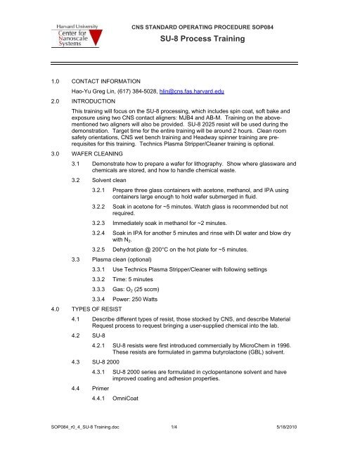
SU-8 Process Training
SU-8 Process Training
SU-8 Process Training

Create successful ePaper yourself
Turn your PDF publications into a flip-book with our unique Google optimized e-Paper software.
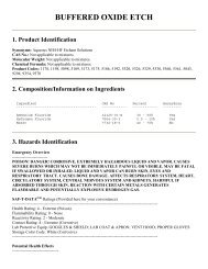
CNS STANDARD OPERATING PROCEDURE SOP084<strong>SU</strong>-8 <strong>Process</strong> <strong>Training</strong>1.0 CONTACT INFORMATIONHao-Yu Greg Lin, (617) 384-5028, hlin@cns.fas.harvard.edu2.0 INTRODUCTIONThis training will focus on the <strong>SU</strong>-8 processing, which includes spin coat, soft bake andexposure using two CNS contact aligners: MJB4 and AB-M. <strong>Training</strong> on the abovementionedtwo aligners will also be provided. <strong>SU</strong>-8 2025 resist will be used during thedemonstration. Target time for the entire training will be around 2 hours. Clean roomsafety orientations, CNS wet bench training and Headway spinner training are prerequisitesfor this training. Technics Plasma Stripper/Cleaner training is optional.3.0 WAFER CLEANING3.1 Demonstrate how to prepare a wafer for lithography. Show where glassware andchemicals are stored, and how to handle chemical waste.3.2 Solvent clean3.2.1 Prepare three glass containers with acetone, methanol, and IPA usingcontainers large enough to hold wafer submerged in fluid.3.2.2 Soak in acetone for ~5 minutes. Watch glass is recommended but notrequired.3.2.3 Immediately soak in methanol for ~2 minutes.3.2.4 Soak in IPA for another 5 minutes and rinse with DI water and blow drywith N 2 .3.2.5 Dehydration @ 200°C on the hot plate for ~5 minutes.3.3 Plasma clean (optional)3.3.1 Use Technics Plasma Stripper/Cleaner with following settings3.3.2 Time: 5 minutes3.3.3 Gas: O 2 (25 sccm)3.3.4 Power: 250 Watts4.0 TYPES OF RESIST4.1 Describe different types of resist, those stocked by CNS, and describe MaterialRequest process to request bringing a user-supplied chemical into the lab.4.2 <strong>SU</strong>-84.2.1 <strong>SU</strong>-8 resists were first introduced commercially by MicroChem in 1996.These resists are formulated in gamma butyrolactone (GBL) solvent.4.3 <strong>SU</strong>-8 20004.3.1 <strong>SU</strong>-8 2000 series are formulated in cyclopentanone solvent and haveimproved coating and adhesion properties.4.4 Primer4.4.1 OmniCoatSOP084_r0_4_<strong>SU</strong>-8 <strong>Training</strong>.doc 1/4 5/18/2010
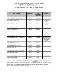
CNS STANDARD OPERATING PROCEDURE SOP084<strong>SU</strong>-8 <strong>Process</strong> <strong>Training</strong>5.0 RESIST DISPENSING5.1 Show where chemicals and supplies are kept, and how to dispose of waste.5.2 Pour the resist directly on the substrate from the bottle for thick resist.5.3 For more diluted resist such as 2002 and 2005, pour the resist in a small disposalcup first before pouring on the samples.5.4 If bubbles are observed in the bottle, you can heat the resist bottle in an uprightposition (50 – 60°C) for 30 minutes, which will reduce the viscosity and allow thebubbles to rise out of solution. Once the bubbles have been removed, allow theresist to reach room temperature prior to use.6.0 SPIN RECIPE6.1 Step 1Speed (rpm) Time (s) Ramp (rpm/s)500 5 1006.2 Step 2Speed (rpm) Time (s) Ramp (rpm/s)3000 30 3007.0 SOFT BAKE7.1 Pre-bake @ 65°C hotplate first then move to 95°C hotplate to prevent suddenthermal expansion. (<strong>Process</strong> is also applicable for cooling.)7.2 Suggested process condition for different types of <strong>SU</strong>-8.<strong>SU</strong>-8 TypePre-Bakeat 65°C(minutes)Pre-Bakeat 95°C(minutes)SuggestedExposure Energy(mJ/cm 2 )Post-ExpBake at 65°C(minutes)Post-Exp Bakeat 95°C(minutes)2 1 1 85 1 12002 1 2 85 1 15 1 3 100 1 12005 1 2 100 1 110 2 5 140 1 2.52010 1 2 140 1 2.52015 1 2 160 1 2+12025 1 3 200 1 3+150 5 15 280 1 4+12050 3 6 310 1 7+12100 5 20 430 1 10+1SOP084_r0_4_<strong>SU</strong>-8 <strong>Training</strong>.doc 2/4 5/18/2010
CNS STANDARD OPERATING PROCEDURE SOP084<strong>SU</strong>-8 <strong>Process</strong> <strong>Training</strong>8.0 EDGE BEAD REMOVAL (EBR)8.1 Step 1Speed (rpm) Time (s) Ramp (rpm/s)400 60 1008.2 Reflow the dissolved <strong>SU</strong>-8 by spin at 1500 rpm for 20 seconds.8.3 Heat wafer on 65°C hotplate for 1 minute, followed by anneal on the 95°Chotplate for another 3 minutes.9.0 EXPO<strong>SU</strong>RE9.1 MJB4 (constant power)9.1.1 Minimum feature size is ~1 um9.1.2 Maximum sample size is 4” wafer9.1.3 Maximum mask size is 5”9.2 AB-M (constant intensity)9.2.1 Minimum feature size is between 1.5 to 2 um9.2.2 Maximum sample size is 4” wafer9.2.3 Maximum mask size is 5”9.3 Calculate the exposure time9.3.1 Exposure energy (resist dosage) / Light intensity (light source) =Exposure Time(mJ / cm 2 ) / (mW / cm 2 ) = seconds9.3.2 For the resist dosage, we use the mid-value for calculation.9.3.3 For <strong>SU</strong>-8 process, a glass plate (360 nm long pass filter) is used to blockwavelength below 360 nm. The <strong>SU</strong>-8 resist polymerizes faster whenexposed to shorter wavelength light (< 350 nm). This being the case, theupper layer of <strong>SU</strong>-8 becomes overexposed and prevents the remaining<strong>SU</strong>-8 material from fully polymerizing. The result is the T-Topping effect.Hence when using the filter, we need to increase the calculatedexposure time by 40% to compensate for the loss of light intensity.9.4 Photolithography steps9.4.1 Describe various aligner states and modes.9.4.2 WEC (wedge error compensation) contact.9.4.3 Separation.9.4.4 Alignment.9.4.5 WEC contact again / exposure contact.9.4.6 Check alignment.SOP084_r0_4_<strong>SU</strong>-8 <strong>Training</strong>.doc 3/4 5/18/2010
CNS STANDARD OPERATING PROCEDURE SOP084<strong>SU</strong>-8 <strong>Process</strong> <strong>Training</strong>10.0 POST EXPO<strong>SU</strong>RE BAKE10.1 Please check table in section 7.2 above for the process condition.11.0 DEVELOPMENT11.1 Demonstrate development in <strong>SU</strong>-8 developer or PGMEA. Expecteddevelopment times vary between different types of resist.11.2 Demonstrate optical inspection of developed wafer/sample using Olympus opticalmicroscope. Point out indications of under or over-developed features.12.0 HARD BAKE (OPTIONAL)12.1 Hard bake temperature: 140°C – 150°C.12.2 Time: 30 minutes12.3 Explain how hard bake improves adhesion between <strong>SU</strong>-8 and substrate. Afterhard bake the resist will not be removed from the substrate during PDMS micromolding.12.4 The hard bake step is also useful for annealing any surface cracks that may beevident after development to produce a smoother surface/side edge.13.0 ADDITIONAL NOTES13.1 Cleaning13.1.1 Use PGMEA to clean <strong>SU</strong>-8 resist.13.1.2 Use IPA to clean PGMEA.13.2 Resist Removal13.2.1 Before exposure, PGMEA can be used to clean resist.13.2.2 O 2 plasma clean (Technics Plasma Stripper/Cleaner) can also be used atlow power (~60 Watts).13.2.3 Once exposure is done, <strong>SU</strong>-8 is almost impossible to remove.14.0 CLEAN-UP15.0 REVISION HISTORYRevision#Date Author (s) Changes/Additions0.0 3/26/10 HL Initial issue.0.1 5/14/10 EM Fixed title header, added captions, compressed.0.2 5/17/10 HL Clerical and notes regarding additional detail.0.3 5/18/10 EM Clerical.0.4 5/18/10 HL Clerical.------------ END OF DOCUMENT ------------SOP084_r0_4_<strong>SU</strong>-8 <strong>Training</strong>.doc 4/4 5/18/2010