+ R - Center for Nanoscale Systems - Harvard University
+ R - Center for Nanoscale Systems - Harvard University
+ R - Center for Nanoscale Systems - Harvard University
- No tags were found...

You also want an ePaper? Increase the reach of your titles
YUMPU automatically turns print PDFs into web optimized ePapers that Google loves.
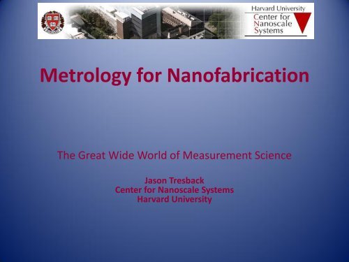
Metrology <strong>for</strong> NanofabricationThe Great Wide World of Measurement ScienceJason Tresback<strong>Center</strong> <strong>for</strong> <strong>Nanoscale</strong> <strong>Systems</strong><strong>Harvard</strong> <strong>University</strong>
Outline• Overview of Metrology– Introduction to Metrology– Metrology <strong>for</strong> Process Control• Key Metrology Techniques <strong>for</strong> Nanofabrication at CNS– Optical Microscopy– Ellipsometry– Profilometry– Atomic Force Microscopy (AFM/SPM)– Thin Film Characterization Part-1• Electrical Property Measurements at CNS– Electronic Conduction Overview– Van der Pauw Resistivity and Hall Measurements– Thin Film Characterization Part-2– Device Testing• Q/A
IntroductionMetrology:The Science of Measurement(Experimental and Theoretical Data w/ Any Certainty)-Scientific, Industrial, and Legal(?-1799)d1 Meter (metre) = Million Microns = Billion Nanometers = ?Traceability:-How Certain Are You About a Measurement or EachStep of a Process?-The Ability to Identify Entities and Verify WithDocumented Records and/or Calibration DataCalibration:-Use of a Traceable Standard (NIST, BIPB,…) toDetermine a Tool’s Bias, Accuracy, and Precision“There are two possible outcomes: if the resultconfirms the hypothesis, then you've made ameasurement. If the result is contrary to thehypothesis, then you've made a discovery. “Enrico Fermi(1889-1960)1 metre = d/10,000,000Wikipedia.orgPt/Ir (1960-1983)Krypton-86Wikipedia.org(1983)Speed of Light
lowProbabilityDistributionAccuracyhighMetrology <strong>for</strong> Process Controlx xx xxxxxxxxxxxAccuracy: (True Value)-How Close to Reference orActual ValuePrecision: (Repeatability)-Degree of Reproducibilityof a MeasurementReference/ActualAccuracyhighPrecisionlowPrecision
Metrology <strong>for</strong> Process ControlDATADesign, Model, andSimulationMetrology:Optical Microscopy (OM)Profilometry, Ellipsometry, 4-PPStation, Rs-Mapper, AFM/SPM…Cost?Destructive?Nanofabrication Process:(Front-end, Lithography, RIE,CVD, PVD, ALD, RTA, Backend…)DATAYield and Per<strong>for</strong>mancePrecision?Speed?DATAMetrology:Stress Tests, Spectroscopy(Raman/FTIR/PL/XPS..), XRD,SIMS, SEM, TEM,DATA-Statistical ProcessControl (SPC)-Standard Deviation
Key Metrology Techniques <strong>for</strong>Nanofabrication at CNS•Optical Microscopy•Ellipsometry•Profilometry•Atomic Force Microscopy (AFM/SPM)•Electrical Characterization•X-Ray Photoelectron Spectroscopy (XPS)•SEM, FIB, and TEM•FTIR, Raman, Photoluminescence,…•X-Ray Diffraction (XRD)•Secondary Ion Mass Spectroscopy (SIMS)•…
Optical MicroscopyCapabilities– More than 10 OMs at CNS: Stereo, Reflection,Transmission, Inverted, Fluorescence….– Modes: BF, DF, Differential Interference Contrast(DIC), Polarizing– Objective Lenses: 2.5x to 150x– Ultra-High Definition Digital Cameras (6.7um/pixel)-Advance Optical Techniques: NSOM, Confocal, TIRF,TRPL, Raman,…(Contact Jiangdong Deng or Arthur McClelland)Advantages– Rapid– Non-destructive– Lager Area InspectionDisadvantages– Lateral Resolution is Limited by Rayleigh Criterion– Poor Vertical Resolution and No Height (Z)In<strong>for</strong>mation100xαR = 0.61λ/ NAN.A = n*sin α0.2 mm WDNA ~ 0.8-0.9520x
Optical Microscopy20x50x50xLateral Measurements:1um or Less but +-0.5um1+mm50x 100xspi.comStage Micrometer’s <strong>for</strong> Routine Manual CalibrationPhotolithography Masks (Steve Hickman)
EllipsometryCapabilities-Polarized Light <strong>for</strong> Multi-Layer Film Thickness (t)and Refractive Index (n)-Works Well <strong>for</strong> Oxide/Nitride/Polymer down to1nm ThicknessAdvantages-Rapid-Non-destructive-200mm Scan Size <strong>for</strong> Large Area Uni<strong>for</strong>mityDisadvantages-Requires Transparent Films (No Metals > 10nm)-Must Have n, t, and K Standardized Values-Interface Must be Clean, No High Roughness–Data Analysis Difficulties:Int.- film is ultra thick (>10um)- ultra thin (1nm)- strong absorption or scatteringr / r tan( )epsThickness (nm)Measured Parameters: tanΨ and CosΔi
EllipsometryGaertner Single WavelengthScanning Ellipsometer (ES-2)J.A Woollam WVASE32 (ES-1)150nm SiO 2 on SiliconRefractive Index (n)30nm SiO 2 on Silicon
ProfilometryTwo Main Types of Profilometry:1) Contact/Stylus Surface Profilometer-Veeco Dektak 6M and KLA-Tencor P16 (PL-3/4/5)-Vertical Step Height (SH): 5nm to 260um-Scan Size: 100um to 50mm-Lateral Resolution: 1-2umDektak 6MCCI HD2) Optical (Interferometer) Surface Profiler-Veeco WykoNT1100 and Taylor Hobson CCI HD (PL-2/6)-Vertical Step Height (SH): 0.1nm to 2mm-Scan Size/Area: 130um to 100mm-Auto Focus/Fringe Find/Scan-Local Film Thickness Measurement: 50nm to 20+umNew Tool at CNS!
Contact Surface ProfilometryDektakmanual.pdfBruker-axs.comLVDT5 umBruker-axs.comWikipedia.orgLinear Variable Differential Trans<strong>for</strong>mer (LVDT)or Displacement Transducer
Optical ProfilometryCCI HDWyko NT1100Taylor Hobson CCI HD.pdfTaylor Hobson CCI HD.pdf
Optical ProfilometryCr/NiFe on Si/Ti/Au5nm-Cr 40nm-NiFeNiFe-40nmCr-5nmSiAuTi
Optical ProfilometryAuTiSiNiFe-40nmCr-5nm
Optical ProfilometryMicro-DotsStitchingSH Calibration Standard 5.183um
Optical ProfilometryElectrode Arrays and Photonic Devices
Atomic Force Microsopy (AFM)4 AFM systems at CNS:-Asylum Research MFP3D-SA-Asylum Research MFP3D-BiO-Veeco NanoMan V-WiTec NSOM/Confocal/Raman/SPM-Environment Control-Nano IndentationCombined FluorescenceMicroscopy <strong>for</strong> Bio-AFMCapabilities and Advantages-Vertical resolution:
Atomic Force Microsopy (AFM)Sub-Micron RIE on Silicon (Nanoman V AFM)Silicon:-1um Grating-2um Pitch~250nm RIE(Ling Xie)
Atomic Force Microsopy (AFM)RIE on Silicon (Nanoman V AFM)5x5um x 200nm Deep Squares/RIE in Silicon
Atomic Force Microsopy (AFM)Ti/Au on p-Silicon (Nanoman V AFM)AuAuSiAu-75nmTi-5nmRMS (Rq):2.97-3.2 nm
Atomic Force Microsopy (AFM)Ti/Au on p-Silicon (MFP3d AFM)NiFeAuNiFeRMS:4.11nmAuTiSiNiFe-40nmCr-5nm
Atomic Force Microsopy (AFM)Si12 umAuAudz = 74.71 nmSiAu-75nmTi-5nm
Thin Film Characterization-1250 °CGrowthRMS:5.06nm250 °CGrowthRMS:4.69nmt = 62.6nmn = 2.48TiO 2 0114 As GrownZnO and TiO 2 Thin FilmDeposition on Si Using ALD(Mac Hathaway)TiO 2 0114 After 550 °C Anneal/30 Minutes150 °CGrowthRMS:1.08nmt = 24.6nmn = 2.24TiO 2 0404 After 550 °C Anneal 30 minutes
Thin Film Characterization-1200 °CGrowthRMS:0.55nmt = 54.3nmn = 1.79ZnO 1006b (550 °C Anneal/30 Minutes)Al-Doped(AZO)RMS:0.60nm200 °CGrowthRMS:1.30nmt = 102.4nmn = 1.97ZnO 111109 (550 °C Anneal/30 Minutes)200 °CGrowtht = 54.3nmn = 1.79
Electrical Property Measurementsat CNS•Electronic Conduction Overview•Van der Pauw Resistivity and Hall Measurement•Thin Film Electrical Characterization•Device Testing•Scanning Probe Microscopy: EFM, CFM, MFM, and SCM•Time Resolved Photoluminescence (TRPL)•Mercury Probe C-V (Non-destructive CV, Hall…)•Deep Level Transient Spectroscopy (DLTS)•Stress Test/Failure Analysis (FA)•…
Electronic ConductionHummel, R.E. Electronic Properties of Materials 3 rd Ed. Springer (2001)Classical Electron TheoryV = I*RBulkQuantum Mechanicsj = σε = I/A = Nve2-d Sheetσ = 1/3v f2 e 2 τN(E f )σ = N f e 2 τ/mALWtρ = 1/σR = ρ(L/A) = ρ(L/t*W) = ρ/t(L/W) = R s (L/W)
Electronic ConductionClassical “Free”Electron Theory-Partially-FilledValence BandMetals and Alloysρ 2 = ρ 1 [1+ α(T 2 – T 1 )]ρ = ρ th + ρ imp + ρ def= ρ th + ρ resIntrinsicSemiconductorsj = σε = I/A = Nveσ = N e u e e + N h u h e-Filled Valence Band-Small Energy Gap toConduction BandHummel, R.E. Electronic Properties of Materials 3 rd Ed. Springer (2001)ExtrinsicSemiconductorsCovalent MaterialsHave Mixed s and pHybrid State’s
Electronic ConductionIntrinsic Semiconductorsj = σε = I/A = Nveσ = N e μ e e + N h μ h eμ = v f /εExtrinsic Semiconductorsσ = N d μ e e + N A μ h en-type SiliconCovalent MaterialsHave s and p HybridState’sσ = 4.84E15 (m e */m o ) 3/2 T 3/2 e(μ e + μ h ) exp[-(E g /2k b T)]Tune E g withDopant/DefectsHummel, R.E. Electronic Properties of Materials 3 rd Ed. Springer (2001)
Electronic ConductionContact Electrode Deployment on Extrinsic Semiconductorsn-typep-typeDiffusion CurrentLower Work FunctionElement ɸ eVAg 4.5-4.7Al 4.1-4.3Ti 4.3Cr 4.5Hg 4.5Si 4.6-4.8In 4.1Space Charge LayersHummel, R.E. Electronic Properties of Materials 3 rd Ed. Springer (2001)Drift CurrentHigher Work FunctionElement ɸ eVAu 5.1-5.5Co 5Pt 5.1-5.9W 4.3-5.2Pd 5.2-5.6Cu 4.5-5.1C 5
Van der Pauw Hall and ResistivityMeasurements1ALV4 14VL1 mmVL123A2 3 2A34R A = V 43 /I 12 R B = V 14 /I 23Van der Pauw Equation: exp(-πR A /R S ) + exp(-πR B /R S ) = 1Ideal Case:R 21,34 = R 12,43R 32,41 = R 23,14 R 43,12 = R 34,21R 14,23 = R 41,32R A = (R 21,34 + R 12,43 + R 43,12 + R 34,21 )/4R B = (R 32,41 + R 23,14 + R 14,23 + R 41,32 )/4DR S = π/ln2*V 23 /I 14= 4.532 (V 23 /I 14 )CDE ResMap (MET-2)40 um WC Tip100 g <strong>for</strong>ce
Van der Pauw Hall and ResistivityMeasurements1ALV4 14VL1 mmVL123A2 3 2A34R A = V 43 /I 12 R B = V 14 /I 23Van der Pauw Equation: exp(-πR A /R S ) + exp(-πR B /R S ) = 1Ideal Case:R 21,34 = R 12,43R 32,41 = R 23,14 R 43,12 = R 34,21R 14,23 = R 41,32R A = (R 21,34 + R 12,43 + R 43,12 + R 34,21 )/4R B = (R 32,41 + R 23,14 + R 14,23 + R 41,32 )/4DR S = π/ln2*V 23 /I 14= 4.532 (V 23 /I 14 )CDE ResMap (MET-2)40 um WC Tip100 g <strong>for</strong>ce
Van der Pauw Hall and ResistivityMeasurements1.4 Tesla (Variable)
Van der Pauw Hall and ResistivityMeasurementsn s = (I*B)/(q*|V H |)ρ = 1/q(nμ n + ημ h )µ = |V H |/(R S I*B) = 1/(q*n S R S ).bulk resistivity (ρ = R S d) and the bulk density (n = n S /d).SampleGlass Cold Finger300K to 100K(~30 mins!)LISE G27300K to 700K(~30 mins!)
Van der Pauw Hall and ResistivityMeasurements10 mm x 10 mm Max Sample SizeL8.5 mm x 8.5 mm Max Sample SizeLCloverleaf Geometry7.5 mm <strong>Center</strong> to <strong>Center</strong>Spacing Recommended7.5 mm <strong>Center</strong> to <strong>Center</strong>Spacing RecommendedDdDD = 1 mm is recommended:(D/L) α error(d/L) α errorD = 1 mm is recommended:(D/L) α errorOk! Better!! Best!!!
Thin Film ElectricalCharacterizationScanning Capacitance Microscopy (SCM) Using AFMTrapped Charges
Thin Film ElectricalCharacterizationN d (x d ) = - C 3 / (qK s ε o A 2 dC/dV)Agilent b1500 w/ MF-CMUC = ε o ε a A/d
Thin Film ElectricalCharacterizationAgilentEasyExpertSoftwareAgilent 4156cw/ 4x HRSMUAgilent b1500w/ MF-CMULakeShore 1.5K Probe StationSignatone 4ptProbe StationRT up to 450K1.5K up to 450 K
Resistivity (ohm-cm)Thin Film Characterization-2AuTiAl-ZnO (AZO)SiO 2SiZnO and TiO 2 Thin Film Depositionon Si Using ALD (Mac Hathaway)AFM (Height)4.0E-02Resisitivity Vs. Temperature3.0E-022.0E-021.0E-020.0E+000 200 400 600 800Temperature (K)ZnO 1006b (550 C Anneal/30 Minutes)
Thin Film Characterization-2AuTiAl-ZnO (AZO)SiO 2SiZnO and TiO 2 Thin Film Depositionon Si Using ALD (Mac Hathaway)AFM (Height)Temperature (K)Resistivity(ohm-cm)Mobility(cm2/Vs)Density (cm-3)100 3.62E-02 -2.39 7.20E+19200 3.04E-02 -2.79 7.30E+19300 2.69E-02 -3.09 7.64E+19300 2.70E-02 -2.91 7.92E+19400 2.20E-02 -3.2 8.82E+19500 1.77E-02 -4.38 8.02E+19600 1.39E-02 -3.06 1.46E+20ZnO 1006b (550 C Anneal/30 Minutes)
Mobility (cm2/V*s)Resistivity (ohm-cm)Carrier Density (cm-3)Thin Film Characterization-2Resisitivity Vs. TemperatureCarrier Density Vs. Temperature5.57.0E+164.53.52.5275 325 375 425Temperature (K)5.0E+163.0E+161.0E+16275 325 375 425Temperature (K)Mobility Vs. Temperature82.562.542.522.52.5275 325 375 425Temperature (K)P-type Silicon with Au/Pt ContactsTemperature (K)Resistivity(ohm-cm)Mobility(cm2/V*s) Density (cm-3)300 3.38 63.0 2.93E+16325 3.69 45.0 3.75E+16350 4 33.6 4.63E+16375 4.32 25.9 5.55E+16400 4.63 20.7 6.48E+16
Thin Film Characterization-2150 °CGrowthRMS:1.08nmt = 24.6nmn = 2.24TiO 2 0404 (550 °C Anneal/30 minutes)200 °CGrowthRMS:1.30nmt = 102.4nmn = 1.97ZnO 111109 (550 °C Anneal/30 Minutes)Photoluminescence Spectroscopy (PL) (Arthur McClelland)
Device Testing1 & 2-d NanoElectronicsM—O—MAuAu0.5 umNiOMetal-Oxide-Metal (MOM)AuNiO, TiO 2 , SnO 2 …Au2 umTresback, et. al. IEEE Transactions on Nanotechnology, 6 [6] 676-81 (2007)
Device Testing1 & 2-d NanoElectronicsM—O—MAuAu0.5 umNiOMetal-Oxide-Metal (MOM)“Failure”NiO, TiO 2 , SnO 2 …AuAu2 um10 umTresback, et. al. IEEE Transactions on Nanotechnology, 6 [6] 676-81 (2007)
Questions?