Combinatorial and High-Throughput Screening of Materials ...
Combinatorial and High-Throughput Screening of Materials ...
Combinatorial and High-Throughput Screening of Materials ...

You also want an ePaper? Increase the reach of your titles
YUMPU automatically turns print PDFs into web optimized ePapers that Google loves.
ACS <strong>Combinatorial</strong> Science<br />
REVIEW<br />
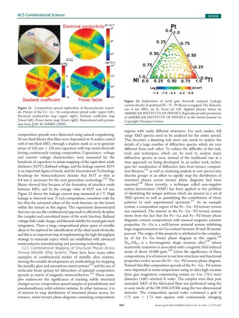
Figure 21. Composition spread exploration <strong>of</strong> thermoelectric materials.<br />
Picture <strong>of</strong> the Co Ce Sn composition spread wafer (upper left);<br />
Electrical conductivity map (upper right); Seeback coefficient map<br />
(lower left); Power factor map (lower right). Reproduced with permission<br />
from JJAP 48, 05EB02 (2009).<br />
composition spreads were fabricated using natural cosputtering.<br />
50 nm thick library thin films were deposited on Si wafers coated<br />
with 6-nm-thick HfO 2 through a shadow mask so as to generate<br />
arrays <strong>of</strong> 250 μm 250 μm capacitors with top metal electrode<br />
having continuously varying composition. Capacitance voltage<br />
<strong>and</strong> current voltage characteristics were measured for the<br />
hundreds <strong>of</strong> capacitors to attain mapping <strong>of</strong> the equivalent oxide<br />
thickness (EOT), flatb<strong>and</strong> voltage, <strong>and</strong> the leakage current. EOT<br />
is an important figure <strong>of</strong> merit, <strong>and</strong> the International Technology<br />
Roadmap for Semiconductors dictates that EOT as thin as<br />
0.8 nm is necessary for the next generation technology. 232 The<br />
library showed that because <strong>of</strong> the formation <strong>of</strong> interface oxide<br />
between HfO 2 <strong>and</strong> Si, the average value <strong>of</strong> EOT was 1.9 nm.<br />
Figure 22 shows the leakage current map measured at 1 V. <strong>High</strong><br />
leakage is observed near Ti-rich composition, consistent with the<br />
fact that the extracted values <strong>of</strong> the work function are the lowest<br />
within the ternary in this region. This experiment demonstrated<br />
that one can use the combinatorial approach to effectively decipher<br />
the complex <strong>and</strong> convoluted issues <strong>of</strong> the work function, flatb<strong>and</strong><br />
voltage shift, oxide charge, <strong>and</strong> thermal stability for metal gate stack<br />
integration. There is large compositional phase space <strong>of</strong> metallic<br />
alloys to be explored for identification <strong>of</strong> the ideal metal electrode,<br />
<strong>and</strong> this is an important step in implementing the high-throughput<br />
strategy to materials topics which are established with advanced<br />
semiconductor manufacturing <strong>and</strong> processing technologies.<br />
3.2.3. <strong>Combinatorial</strong> Mapping <strong>of</strong> Structural Phases Across<br />
Ternary Metallic Alloy Systems. There have been many other<br />
examples <strong>of</strong> combinatorial studies <strong>of</strong> metallic alloy systems.<br />
Among the notable developments are methodology for mapping<br />
the metallic glass <strong>and</strong> amorphous metal systems 233 <strong>and</strong> the use <strong>of</strong><br />
molecular beam epitaxy for fabrication <strong>of</strong> epitaxial composition<br />
spreads in search <strong>of</strong> magnetic semiconductors. 234 These examples<br />
underscore the significance <strong>of</strong> tracking subtle structural<br />
changes across composition spread samples in pseudobinary <strong>and</strong><br />
pseudomultinary solid solution systems. In other instances, it is<br />
<strong>of</strong> interest to map distribution <strong>of</strong> structural phases across, for<br />
instance, entire ternary phase diagrams containing compositions<br />
Figure 22. Exploration <strong>of</strong> novel gate electrode material. Leakage<br />
current density <strong>of</strong> sputtered Ni Ti Pt library is mapped. The dielectric<br />
was 6 nm HfO 2 on Si. From ref 230. Applied physics letters by<br />
AMERICAN INSTITUTE OF PHYSICS. Reproduced with permission<br />
<strong>of</strong> AMERICAN INSTITUTE OF PHYSICS. in the format Journal via<br />
Copyright Clearance Center.<br />
regions with vastly different structures. For such studies, full<br />
range XRD spectra need to be analyzed for the entire spread.<br />
This becomes a daunting task since one needs to analyze the<br />
details <strong>of</strong> a large number <strong>of</strong> diffraction spectra which are very<br />
different from each other. To reduce the difficulty <strong>of</strong> this task,<br />
tools <strong>and</strong> techniques, which can be used to analyze many<br />
diffraction spectra at once, instead <strong>of</strong> the traditional one at a<br />
time approach are being developed. In an earlier work, techniques<br />
for visualization <strong>of</strong> diffraction data from ternary composition<br />
libraries, 235 as well as clustering analysis to sort spectra into<br />
discrete groups in an effort to rapidly map the distribution <strong>of</strong><br />
structural phases across ternary phase diagrams had been<br />
reported. 236 More recently, a technique called non-negative<br />
matrix factorization (NMF) has been applied to the problem<br />
<strong>of</strong> identifying the unique patterns which are present in a set <strong>of</strong><br />
XRD spectra as well as quantifying the contribution <strong>of</strong> those<br />
patterns to each experimental spectrum. 237 As an example<br />
system, a composition region <strong>of</strong> the Fe Ga Pd ternary system<br />
was examined. The interest in the Fe Ga Pd ternary system<br />
stems from the fact that the Fe Ga <strong>and</strong> Fe Pd binary phase<br />
diagrams contain compositions with unusual magnetic actuator<br />
properties. Fe Ga is a well-known material system exhibiting<br />
large magnetostriction for Ga content between 20 <strong>and</strong> 30 atomic<br />
percent. The origin <strong>of</strong> this property is attributed to the complexity<br />
<strong>of</strong> the Fe Ga binary phase diagram in this region. 238<br />
Fe 0.7 Pd 0.3 is a ferromagnetic shape memory alloy 239 whose<br />
martensitic transition is associated with a magnetic field induced<br />
strain <strong>of</strong> about 10 000 ppm. 240 Given the significance <strong>of</strong> these<br />
compositions, it is <strong>of</strong> interest to see how structures <strong>and</strong> functional<br />
properties evolve across the Fe Ga Pd ternary phase diagram.<br />
Natural thin film composition spreads <strong>of</strong> the Fe Ga Pd system<br />
were deposited at room temperature using an ultra high-vacuum<br />
three gun magnetron cosputtering system on 3-in. (76.2 mm)<br />
diameter (100) oriented Si wafer. The samples were then post<br />
annealed. XRD <strong>of</strong> the fabricated films was performed using the<br />
ω-scan mode <strong>of</strong> the D8 DISCOVER using the two-dimensional<br />
detector. The composition spread wafer contained a grid <strong>of</strong><br />
1.75 mm 1.75 mm squares with continuously changing<br />
602 dx.doi.org/10.1021/co200007w |ACS Comb. Sci. 2011, 13, 579–633