IntelR 80960 RN I/O Processor Datasheet
IntelR 80960 RN I/O Processor Datasheet
IntelR 80960 RN I/O Processor Datasheet

Create successful ePaper yourself
Turn your PDF publications into a flip-book with our unique Google optimized e-Paper software.
Intel ® <strong>80960</strong><strong>RN</strong> I/O <strong>Processor</strong><br />
2.2 Intel ® i960 ® Core Features (Intel ® <strong>80960</strong>JT)<br />
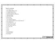
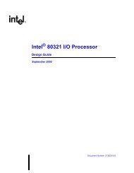
The processing power of the <strong>80960</strong><strong>RN</strong> processor comes from the 100 MHz <strong>80960</strong>JT processor<br />
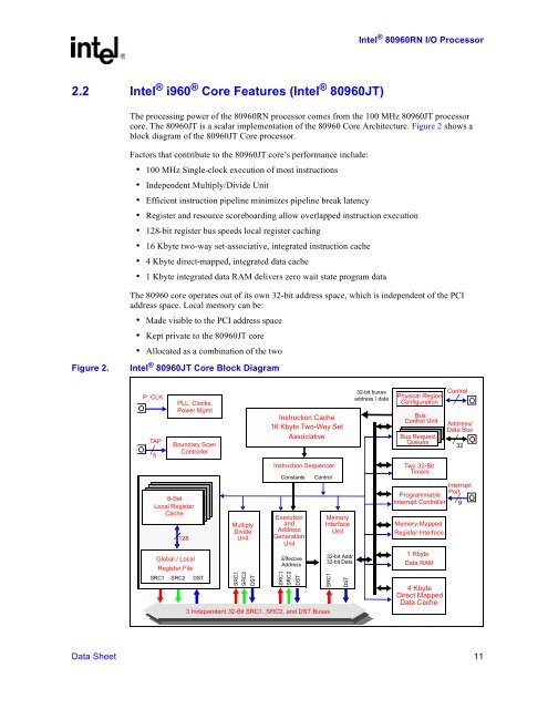
core. The <strong>80960</strong>JT is a scalar implementation of the <strong>80960</strong> Core Architecture. Figure 2 shows a<br />
block diagram of the <strong>80960</strong>JT Core processor.<br />
Factors that contribute to the <strong>80960</strong>JT core’s performance include:<br />
• 100 MHz Single-clock execution of most instructions<br />
• Independent Multiply/Divide Unit<br />
• Efficient instruction pipeline minimizes pipeline break latency<br />
• Register and resource scoreboarding allow overlapped instruction execution<br />
• 128-bit register bus speeds local register caching<br />
• 16 Kbyte two-way set-associative, integrated instruction cache<br />
• 4 Kbyte direct-mapped, integrated data cache<br />
• 1 Kbyte integrated data RAM delivers zero wait state program data<br />
Figure 2.<br />
The <strong>80960</strong> core operates out of its own 32-bit address space, which is independent of the PCI<br />
address space. Local memory can be:<br />
• Made visible to the PCI address space<br />
• Kept private to the <strong>80960</strong>JT core<br />
• Allocated as a combination of the two<br />
Intel ® <strong>80960</strong>JT Core Block Diagram<br />
P_CLK<br />
TAP<br />
5<br />
PLL, Clocks,<br />
Power Mgmt<br />
Boundary Scan<br />
Controller<br />
8-Set<br />
Local Register<br />
Cache<br />
128<br />
Global / Local<br />
Register File<br />
SRC1 SRC2 DST<br />
Multiply<br />
Divide<br />
Unit<br />
SRC1<br />
SRC2<br />
DST<br />
Instruction Cache<br />
16 Kbyte Two-Way Set<br />
Associative<br />
Instruction Sequencer<br />
Constants<br />
Execution<br />
and<br />
Address<br />
Generation<br />
Unit<br />
Effective<br />
Address<br />
SRC1<br />
SRC2<br />
DST<br />
Control<br />
3 Independent 32-Bit SRC1, SRC2, and DST Buses<br />
Memory<br />
Interface<br />
Unit<br />
32-bit Addr<br />
32-bit Data<br />
SRC1<br />
DST<br />
32-bit buses<br />
address / data<br />
Physical Region<br />
Configuration<br />
Bus<br />
Control Unit<br />
Bus Request<br />
Queues<br />
Two 32-Bit<br />
Timers<br />
Control<br />
Address/<br />
Data Bus<br />
Interrupt<br />
Programmable<br />
Port<br />
Interrupt Controller 9<br />
Memory-Mapped<br />
Register Interface<br />
1Kbyte<br />
Data RAM<br />
4Kbyte<br />
Direct Mapped<br />
Data Cache<br />
32<br />
Data Sheet 11