IntelR 80960 RN I/O Processor Datasheet
IntelR 80960 RN I/O Processor Datasheet
IntelR 80960 RN I/O Processor Datasheet

Create successful ePaper yourself
Turn your PDF publications into a flip-book with our unique Google optimized e-Paper software.
Intel ® <strong>80960</strong><strong>RN</strong> I/O <strong>Processor</strong><br />
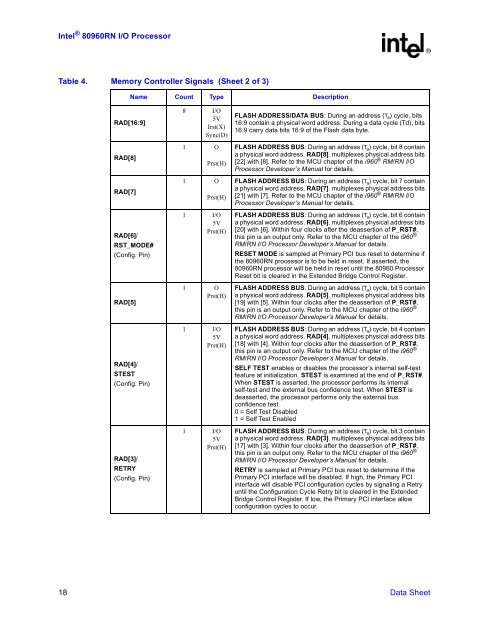
Table 4. Memory Controller Signals (Sheet 2 of 3)<br />
Name Count Type Description<br />
RAD[16:9]<br />
RAD[8]<br />
RAD[7]<br />
RAD[6]/<br />
RST_MODE#<br />
(Config. Pin)<br />
RAD[5]<br />
RAD[4]/<br />
STEST<br />
(Config. Pin)<br />
RAD[3]/<br />
RETRY<br />
(Config. Pin)<br />
8 I/O<br />
5V<br />
Irst(X)<br />
Sync(D)<br />
1 O<br />
Prst(H)<br />
1 O<br />
Prst(H)<br />
1 I/O<br />
5V<br />
Prst(H)<br />
1 O<br />
Prst(H)<br />
1 I/O<br />
5V<br />
Prst(H)<br />
1 I/O<br />
5V<br />
Prst(H)<br />
FLASH ADDRESS/DATA BUS: Duringanaddress(T a ) cycle, bits<br />
16:9 contain a physical word address. During a data cycle (Td), bits<br />
16:9 carry data bits 16:9 of the Flash data byte.<br />
FLASH ADDRESS BUS: During an address (T a ) cycle, bit 8 contain<br />
a physical word address. RAD[8]. multiplexes physical address bits<br />
[22] with [8]. Refer to the MCU chapter of the i960 ® RM/<strong>RN</strong> I/O<br />
<strong>Processor</strong> Developer’s Manual for details.<br />
FLASH ADDRESS BUS: During an address (T a ) cycle, bit 7 contain<br />
a physical word address. RAD[7]. multiplexes physical address bits<br />
[21] with [7]. Refer to the MCU chapter of the i960 ® RM/<strong>RN</strong> I/O<br />
<strong>Processor</strong> Developer’s Manual for details.<br />
FLASH ADDRESS BUS: During an address (T a ) cycle, bit 6 contain<br />
a physical word address. RAD[6]. multiplexes physical address bits<br />
[20] with [6]. Within four clocks after the deassertion of P_RST#,<br />
this pin is an output only. Refer to the MCU chapter of the i960 ®<br />
RM/<strong>RN</strong> I/O <strong>Processor</strong> Developer’s Manual for details.<br />
RESET MODE is sampled at Primary PCI bus reset to determine if<br />
the <strong>80960</strong><strong>RN</strong> processor is to be held in reset. If asserted, the<br />
<strong>80960</strong><strong>RN</strong> processor will be held in reset until the <strong>80960</strong> <strong>Processor</strong><br />
Reset bit is cleared in the Extended Bridge Control Register.<br />
FLASH ADDRESS BUS: During an address (T a ) cycle, bit 5 contain<br />
a physical word address. RAD[5]. multiplexes physical address bits<br />
[19] with [5]. Within four clocks after the deassertion of P_RST#,<br />
this pin is an output only. Refer to the MCU chapter of the i960 ®<br />
RM/<strong>RN</strong> I/O <strong>Processor</strong> Developer’s Manual for details.<br />
FLASH ADDRESS BUS: During an address (T a ) cycle, bit 4 contain<br />
a physical word address. RAD[4]. multiplexes physical address bits<br />
[18] with [4]. Within four clocks after the deassertion of P_RST#,<br />
this pin is an output only. Refer to the MCU chapter of the i960 ®<br />
RM/<strong>RN</strong> I/O <strong>Processor</strong> Developer’s Manual for details.<br />
SELF TEST enables or disables the processor’s internal self-test<br />
feature at initialization. STEST is examined at the end of P_RST#.<br />
When STEST is asserted, the processor performs its internal<br />
self-test and the external bus confidence test. When STEST is<br />
deasserted, the processor performs only the external bus<br />
confidence test.<br />
0 = Self Test Disabled<br />
1 = Self Test Enabled<br />
FLASH ADDRESS BUS: During an address (T a ) cycle, bit 3 contain<br />
a physical word address. RAD[3]. multiplexes physical address bits<br />
[17] with [3]. Within four clocks after the deassertion of P_RST#,<br />
this pin is an output only. Refer to the MCU chapter of the i960 ®<br />
RM/<strong>RN</strong> I/O <strong>Processor</strong> Developer’s Manual for details.<br />
RETRY is sampled at Primary PCI bus reset to determine if the<br />
Primary PCI interface will be disabled. If high, the Primary PCI<br />
interface will disable PCI configuration cycles by signaling a Retry<br />
until the Configuration Cycle Retry bit is cleared in the Extended<br />
Bridge Control Register. If low, the Primary PCI interface allow<br />
configuration cycles to occur.<br />
18 Data Sheet