IntelR 80960 RN I/O Processor Datasheet
IntelR 80960 RN I/O Processor Datasheet
IntelR 80960 RN I/O Processor Datasheet

You also want an ePaper? Increase the reach of your titles
YUMPU automatically turns print PDFs into web optimized ePapers that Google loves.
Intel ® <strong>80960</strong><strong>RN</strong> I/O <strong>Processor</strong><br />
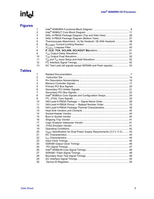
Figures<br />
Tables<br />
1 Intel ® <strong>80960</strong><strong>RN</strong> Functional Block Diagram ..................................................... 8<br />
2 Intel ® <strong>80960</strong>JT Core Block Diagram ............................................................. 11<br />
3 540L H-PBGA Package Diagram (Top and Side View) ................................ 26<br />
4 540L H-PBGA Package Diagram (Bottom View) .......................................... 27<br />
5 Thermocouple Attachment - A) No Heatsink / B) With Heatsink ................... 38<br />
6 V CC5REF Current-Limiting Resistor................................................................ 43<br />
7 V CCPLL Lowpass Filter .................................................................................. 43<br />
8 P_CLK, TCK, DCLKIN, DCLKOUT Waveform............................................. 51<br />
9 T OV Output Delay Waveform......................................................................... 51<br />
10 T OF Output Float Waveform .......................................................................... 52<br />
11 T IS and T IH Input Setup and Hold Waveform ................................................ 52<br />
12 I 2 C Interface Signal Timings.......................................................................... 52<br />
13 AC Test Load (all signals except SDRAM and Flash signals)....................... 53<br />
1 Related Documentation................................................................................... 7<br />
2 Instruction Set .............................................................................................. 14<br />
3 Pin Description Nomenclature....................................................................... 16<br />
4 Memory Controller Signals ............................................................................ 17<br />
5 Primary PCI Bus Signals ............................................................................... 20<br />
6 Secondary PCI Arbiter Signals...................................................................... 21<br />
7 Secondary PCI Bus Signals .......................................................................... 22<br />
8 Intel ® <strong>80960</strong>Jx Core Signals and Configuration Straps................................. 24<br />
9 I 2 C, JTAG, Core Signals ............................................................................... 25<br />
10 540-Lead H-PBGA Package — Signal Name Order ..................................... 28<br />
11 540-Lead H-PBGA Pinout — Ballpad Number Order.................................... 33<br />
12 540-Lead H-PBGA Package Thermal Characteristics .................................. 39<br />
13 Heat Sink Vendors and Contacts .................................................................. 40<br />
14 Socket-Header Vendor.................................................................................. 40<br />
15 Burn-in Socket Vendor .................................................................................. 40<br />
16 Shipping Tray Vendor.................................................................................... 41<br />
17 Logic Analyzer Interposer Vendor ................................................................. 41<br />
18 JTAG Emulator Vendor ................................................................................. 41<br />
19 Operating Conditions..................................................................................... 42<br />
20 V DIFF Specification for Dual Power Supply Requirements (3.3 V, 5 V)......... 43<br />
21 DC Characteristics ........................................................................................ 44<br />
22 I CC Characteristics ........................................................................................ 45<br />
23 Input Clock Timings....................................................................................... 46<br />
24 SDRAM Output Clock Timings ...................................................................... 46<br />
25 PCI Signal Timings....................................................................................... 47<br />
26 Intel ® <strong>80960</strong>JN Core Signal Timings............................................................. 48<br />
27 SDRAM / Flash Signal Timings..................................................................... 48<br />
28 Boundary Scan Test Signal Timings ............................................................. 49<br />
29 I2C Interface Signal Timings ......................................................................... 50<br />
30 Device ID Registers...................................................................................... 54<br />
Data Sheet 5