SOS project Image Manipulation for W f Pl C f i i O i l Wafer ... - JePPIX
SOS project Image Manipulation for W f Pl C f i i O i l Wafer ... - JePPIX
SOS project Image Manipulation for W f Pl C f i i O i l Wafer ... - JePPIX

You also want an ePaper? Increase the reach of your titles
YUMPU automatically turns print PDFs into web optimized ePapers that Google loves.
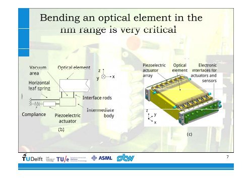
Bending an optical element in the<br />
nm range is very critical<br />
( )<br />
Vacuum<br />
area<br />
Horizontal<br />
leaf spring<br />
Optical element<br />
y<br />
z<br />
x<br />
Piezoelectric<br />
actuator<br />
t<br />
array<br />
Optical<br />
element<br />
Electronic<br />
interfaces <strong>for</strong><br />
actuators and<br />
sensors<br />
Interface rods<br />
Compliance<br />
Piezoelectric<br />
actuator<br />
Intermediate<br />
body<br />
z<br />
y<br />
x<br />
(b)<br />
(c)<br />
Delft<br />
University of<br />
Technology<br />
7