Download "Quadrature Down Conversion . . ."
Download "Quadrature Down Conversion . . ."
Download "Quadrature Down Conversion . . ."

You also want an ePaper? Increase the reach of your titles
YUMPU automatically turns print PDFs into web optimized ePapers that Google loves.
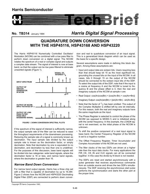
Harris Semiconductor<br />
No. TB314 January 1994<br />
Harris Digital Signal Processing<br />
QUADRATURE DOWN CONVERSION<br />
WITH THE HSP45116, HSP43168 AND HSP43220<br />
The Harris HSP45116 Numerically Controlled Oscillator/<br />
Modulator (NCOM) can be combined with a low pass filter to<br />
perform down conversion on a digital signal. The NCOM<br />
rotates the spectrum of a real or complex signal and outputs<br />
a complex data stream. The signal of interest is now at base<br />
band, so that the output can be low pass filtered to eliminate<br />
unwanted signals (Figure 1).<br />
INPUT SPECTRUM<br />
OUTPUT OF<br />
SIN/COS<br />
GENERATOR<br />
IN NCOM<br />
OUTPUT OF NCOM:<br />
INPUT ROTATED BY ω<br />
OUTPUT OF LOW:<br />
PASS FILTER:<br />
PASS ONLY<br />
BASEBAND SIGNAL<br />
FIGURE 1. DOWN CONVERSION SPECTRAL PLOTS<br />
If the spectrum of the signal of interest is sufficiently narrow,<br />
the output sample rate of the filter can be reduced to ease<br />
the throughput requirements of the downstream processing.<br />
Reducing the sample rate of a signal is commonly known as<br />
decimation. The input sample rate divided by the output<br />
sample rate is known as the decimation factor, or simply<br />
decimation. Note that decimation by one is equivalent to no<br />
decimation, and decimation by less than one is undefined.<br />
For the purposes of this discussion, base band signals will<br />
be divided into two categories: wide band signals, where the<br />
decimation factor is 16 or less, and narrow band signals,<br />
where the decimation is greater than 16.<br />
Narrow Band <strong>Down</strong> <strong>Conversion</strong><br />
SIGNAL OF<br />
INTEREST<br />
e jωt<br />
For narrow band output signals, Harris has a three chip set<br />
with a filter that is capable of decimation by up to 16,384.<br />
Figure 2 shows how the NCOM and HSP43220 Decimating<br />
Digital Filter (DDF) are connected to perform down conver-<br />
sion and real to quadrature conversion of an input signal.<br />
This is a generalized block diagram which can be used as<br />
the basis for a specific design.<br />
Several assumptions were made in defining this block diagram.<br />
Among these assumptions are:<br />
• Input and output data are sixteen bits. Users requiring less<br />
than that should keep bit 15 as the most significant bit,<br />
grounding the unused bits on the input of the NCOM. In all<br />
cases, bits 0 through 15 on the output of the NCOM<br />
should be connected to the sixteen input bits of the DDF.<br />
To select the output bits of the DDF, note that if the input is<br />
a cosine at frequency A and the NCOM is tuned to frequency<br />
B and the phase offset is 0, then the real and<br />
imaginary outputs of the NCOM at sample n are:<br />
• Real Output: cos(An)cos(Bn) = [cos(An-Bn) + cos(An+Bn)]<br />
• Imaginary Output: cos(An)sin(Bn) = [sin(An+Bn) - sin(An-Bn)]<br />
• Note that the factor of 1 / 2 has been omitted. The output of<br />
the Complex Multiplier is shifted left by one bit internally.<br />
For this reason, both the real and imaginary outputs have<br />
the same magnitude as the input.<br />
• The Phase Register is selected to control the phase of the<br />
NCOM (as opposed to MOD0-1) and is initialized along<br />
with the center frequency. In this example, the LOAD# signal<br />
is not exercised, so the initial phase of the NCOM is<br />
unknown.<br />
• To shift the positive component of a real input signal to<br />
base band, the Center Frequency Register of the NCOM<br />
is set to a negative number.<br />
• The Offset Frequency Register, Timer Accumulator and<br />
Complex Accumulator of the NCOM are not used.<br />
• The filter clocks of the two DDFs are driven at a higher<br />
rate than the input data clocks. For many applications the<br />
FIR_CK, CK_IN and CLK signals can all be connected<br />
together. In this case the divide by N block is not needed.<br />
• The DDFs are reset and started asynchronously with a<br />
pulse generator that receives asynchronous commands<br />
from an outside source and drives the two DDFs simultaneously.<br />
The DDF receiving the asynchronous start pulse<br />
performs the synchronization and starts the other part at<br />
the proper time.<br />
Copyright © Harris Corporation 1993<br />
9-46
Tech Brief 314<br />
A/D CONVERTER<br />
16<br />
“0”<br />
RIN16-18<br />
RIN0-15<br />
RO0-15<br />
16<br />
DATA_IN0-15<br />
CK_IN DATA_OUT0-15<br />
16<br />
MICROPROCESSOR<br />
DATA<br />
WE#<br />
ADDRESS<br />
DECODE<br />
“0”<br />
GND<br />
GND<br />
DATA BUS<br />
WE#<br />
ADDRESS BUS<br />
DECODE0<br />
DECODE1<br />
DECODE2<br />
DECODE3<br />
GND<br />
DECODE4<br />
GND<br />
VCC<br />
IMIN0-18<br />
ENI#<br />
SH0-1<br />
C0-15<br />
HSP45116<br />
WR#<br />
AD0-1<br />
CS#<br />
ENPHREG#<br />
ENCFREG#<br />
CLROFR#<br />
MOD0-1<br />
PMSEL<br />
DATA BUS<br />
WE#<br />
ADDRESS BUS<br />
DECODE3<br />
VCC<br />
GND<br />
GND<br />
GND<br />
FIR_CK DATA_RDY<br />
C_BUS0-15<br />
WR#<br />
A0-2 HSP43220<br />
CS#<br />
RESET#<br />
STARTIN#<br />
ASTARTIN#<br />
OUT_SELH#<br />
OUT_ENP#<br />
OUT_ENX#<br />
VCC<br />
GND<br />
VCC<br />
VCC<br />
VCC<br />
VCC<br />
GND<br />
VCC<br />
GND<br />
ENOFREG#<br />
ENPHAC#<br />
LOAD#<br />
PACI#<br />
ENTIREG#<br />
RBYTILD#<br />
MODPI/2PI#<br />
BINFMT#<br />
OUTMUX0-1<br />
IO0-15<br />
16<br />
DATA BUS<br />
WE#<br />
ADDRESS BUS<br />
DECODE4<br />
DATA_IN0-15<br />
CK_IN DATA_OUT0-15<br />
FIR_CK DATA_RDY<br />
C_BUS0-15<br />
WR#<br />
A0-2 HSP43220<br />
CS#<br />
RESET#<br />
16<br />
GND<br />
VCC<br />
GND<br />
VCC<br />
VCC<br />
GND<br />
OER#<br />
OEREXT#<br />
OEI#<br />
OEIEXT#<br />
PEAK#<br />
ACC<br />
RESET<br />
START<br />
PULSE<br />
GENERATOR<br />
VCC<br />
GND<br />
GND<br />
GND<br />
STARTIN# STARTOUT#<br />
ASTARTIN#<br />
OUT_SELH#<br />
OUT_ENP#<br />
OUT_ENX#<br />
CLK<br />
÷N OSCILLATOR<br />
FIGURE 2. BLOCK DIAGRAM FOR QUADRATURE DOWN CONVERSION WITH HSP45116 AND HSP43220.<br />
9-47
Tech Brief 314<br />
A/D CONVERTER<br />
10<br />
“0”<br />
RIN0-5,16-18<br />
RIN6-15<br />
RO6-15<br />
GND<br />
INA0-9<br />
INB0<br />
OUT9-18<br />
MICROPROCESSOR<br />
DATA<br />
WE#<br />
ADDRESS<br />
DECODE<br />
“0”<br />
GND<br />
GND<br />
DATA BUS<br />
WE#<br />
ADDRESS BUS<br />
DECODE0<br />
DECODE1<br />
DECODE2<br />
DECODE3<br />
GND<br />
GND<br />
VCC<br />
VCC<br />
IMIN0-18<br />
ENI#<br />
SH0-1<br />
C0-15<br />
WR#<br />
AD0-1<br />
CS#<br />
ENPHREG#<br />
ENCFREG#<br />
CLROFR#<br />
MOD0-1<br />
PMSEL<br />
ENOFREG#<br />
HSP45116<br />
DATA BUS<br />
ADDRESS BUS<br />
DECODE3<br />
WE#<br />
PAL22V10<br />
GND<br />
GND<br />
GND<br />
VCC<br />
GND<br />
GND<br />
GND<br />
CLK<br />
CSEL0-4<br />
ACCEN<br />
CIN0-9<br />
A0-8<br />
HSP43168<br />
CS#<br />
WR#<br />
RVRS#<br />
FWRD#<br />
MUX1#<br />
MUX0#<br />
SHFTEN#<br />
TXFR#<br />
OEL#<br />
OEH#<br />
GND<br />
VCC<br />
VCC<br />
VCC<br />
VCC<br />
GND<br />
VCC<br />
GND<br />
GND<br />
VCC<br />
GND<br />
VCC<br />
VCC<br />
ENPHAC#<br />
LOAD#<br />
PACI#<br />
ENTIREG#<br />
RBYTILD#<br />
MODPI/2PI#<br />
BINFMT#<br />
OUTMUX0-1<br />
OER#<br />
OEREXT#<br />
OEI#<br />
OEIEXT#<br />
PEAK#<br />
IO6-15<br />
10<br />
DATA BUS<br />
ADDRESS BUS<br />
DECODE3<br />
WE#<br />
GND<br />
GND<br />
GND<br />
GND<br />
VCC<br />
GND<br />
GND<br />
GND<br />
INA0-9<br />
INB0<br />
CLK<br />
CSEL0-4<br />
ACCEN<br />
CIN0-9<br />
A0-8 HSP43168<br />
CS#<br />
WR#<br />
RVRS#<br />
FWRD#<br />
MUX1#<br />
MUX0#<br />
SHFTEN#<br />
TXFR#<br />
OEL#<br />
OEH#<br />
OUT9-18<br />
GND<br />
ACC<br />
OSCILLATOR<br />
CLK<br />
FIGURE 3. BLOCK DIAGRAM FOR WIDE BAND QUADRATURE DOWN CONVERSION WITH HSP45116 AND HSP43168.<br />
9-48
Tech Brief 314<br />
A/D CONVERTER<br />
MICROPROCESSOR<br />
DATA<br />
WE#<br />
ADDRESS<br />
DECODE<br />
“0”<br />
10<br />
“0”<br />
GND<br />
GND<br />
DATA BUS<br />
WE#<br />
ADDRESS BUS<br />
DECODE0<br />
DECODE1<br />
DECODE2<br />
DECODE3<br />
GND<br />
GND<br />
RIN16-18<br />
RO6-15<br />
RIN0-15<br />
IO6-15<br />
IMIN0-18<br />
ENI#<br />
SH0-1<br />
C0-15<br />
HSP45116<br />
WR#<br />
AD0-1<br />
CS#<br />
ENPHREG#<br />
ENCFREG#<br />
CLROFR#<br />
MOD0-1<br />
10<br />
10<br />
DATA BUS<br />
ADDRESS BUS<br />
DECODE3<br />
WE#<br />
PAL22V10<br />
GND<br />
GND<br />
GND<br />
VCC<br />
GND<br />
INA0-9<br />
INB0-9<br />
CLK<br />
CSEL0-4<br />
ACCEN<br />
CIN0-9<br />
A0-8<br />
HSP43168<br />
CS#<br />
WR#<br />
RVRS#<br />
FWRD#<br />
MUX1#<br />
MUX0#<br />
SHFTEN#<br />
TXFR#<br />
OEL#<br />
OEH#<br />
OUT9-18<br />
VCC<br />
VCC<br />
PMSEL<br />
ENOFREG#<br />
GND<br />
ENPHAC#<br />
VCC<br />
LOAD#<br />
VCC<br />
VCC<br />
PACI#<br />
ENTIREG#<br />
REG<br />
I<br />
VCC<br />
GND<br />
RBYTILD#<br />
MODPI/2PI#<br />
Q<br />
VCC<br />
BINFMT#<br />
GND<br />
OUTMUX0-1<br />
GND<br />
OER#<br />
VCC<br />
OEREXT#<br />
GND<br />
OEI#<br />
VCC<br />
OEIEXT#<br />
OSCILLATOR<br />
VCC<br />
GND<br />
PEAK#<br />
ACC<br />
CLK<br />
FIGURE 4. BLOCK DIAGRAM FOR WIDE BAND DOWN CONVERSION WITH HSP45116 AND HSP43168.<br />
9-49
Tech Brief 314<br />
Wide Band <strong>Down</strong> <strong>Conversion</strong><br />
Figures 3 and 4 show how the NCOM and HSP43168 Dual<br />
FIR Filter (Dual FIR) are connected to perform down conversion<br />
and real to quadrature conversion of an input signal.<br />
Because the Dual FIR can implement either one or two filters,<br />
two block diagrams are shown. Figure 3 shows the<br />
case where each 43168 is implementing a single filter. The<br />
maximum number of coefficients in this case is 16 times the<br />
decimation factor for each filter. Figure 4 shows the same<br />
configuration with the exception that the Dual FIR is now<br />
configured as two independent filters, each with a maximum<br />
length of 8 times the decimation factor.<br />
These are generalized block diagrams which can be used as<br />
the basis for a specific design. Note that they do not represent<br />
detailed schematics with all gates represented. For<br />
instance, the control signals are driven with a single<br />
PAL22V10 operating as a self contained state machine; it<br />
reality, the 22V10 may not have enough gates to generate all<br />
the necessary output sequences; in that case, it would be<br />
necessary to have a counter generate the states and use the<br />
PAL to decode the counter output, generate the control signals<br />
to the 43168, and reset the counter when the sequence<br />
is completed.<br />
The design parameters of these circuits are:<br />
• Input data is 10 bits. Users requiring less than that should<br />
keep bit 15 as the most significant bit of the NCOM,<br />
grounding the unused bits on the input. In all cases, bits 6<br />
through 15 on the output of the NCOM should be connected<br />
to the input bits of the Dual. To select the output<br />
bits of the Dual, note that if the input is a cosine at frequency<br />
A and the NCOM is tuned to frequency B and the<br />
phase offset is 0, then the real and imaginary outputs of<br />
the NCOM at sample n are:<br />
• Real Output: cos(An)cos(Bn) = [cos(An-Bn) + cos(An+Bn)]<br />
• Imaginary Output: cos(An)sin(Bn) = [sin(An+Bn) - sin(An-Bn)]<br />
• Note that the factor of 1 / 2 has been omitted. The output of<br />
the Complex Multiplier is shifted left by one bit internally.<br />
For this reason, both the real and imaginary outputs have<br />
the same magnitude as the input.<br />
• The Phase Register is selected to control the phase of the<br />
NCOM (as opposed to MOD0-1) and is initialized along<br />
with the center frequency. In this example, the LOAD# signal<br />
is not exercised, so the initial phase of the NCOM is<br />
unknown.<br />
• To shift the positive component of a real input signal to<br />
base band, the Center Frequency Register of the NCOM<br />
is set to a negative number.<br />
• The Offset Frequency Register, Timer Accumulator and<br />
Complex Accumulator of the NCOM are not used.<br />
• The decimation rate in the Dual FIRs is greater than one.<br />
For no decimation, TXFR# should be grounded. Note that<br />
the maximum number of coefficients in the 43168 is eight<br />
or sixteen times the decimation rate, depending on the<br />
mode (see above).<br />
Combined Narrow And Wide Band<br />
In some applications, it is necessary to pass both wide and<br />
narrow band signals. In this case, both the HSP43220 and<br />
HSP43168 can be used in parallel, with the user selecting<br />
the output of either set of chips, depending on the characteristics<br />
of the signal of interest. Figure 5 shows this application,<br />
with most of the control signals eliminated for clarity.<br />
(These signals can be derived from the previous block diagrams.)<br />
In addition, note that the input data clock (CK_IN)<br />
and the FIR clock (FIR_CK) of the DDF have been connected<br />
together. This configuration is applicable when the<br />
input data rate is sufficiently high to allow the filter to operate<br />
at this rate also. If this is not the case, the divide by N circuit<br />
used in Figure 2 could be used, with the high speed clock<br />
driving the FIR_CK pins and the divided down clock used for<br />
all other clocks in the circuit.<br />
New Products<br />
Now available from Harris are the HSP50016 Digital <strong>Down</strong><br />
Converter, which is a single chip quadrature down converter<br />
and low pass filter (Figure 6). In addition, the HSP43216 Half<br />
Band Filter allows the user to double the input sample rate of<br />
the NCOM for real signals (Figure 7). Contact your local Harris<br />
sales office or representative for more details on these<br />
and other new products from Harris.<br />
9-50
Tech Brief 314<br />
“0”<br />
RIN16-18<br />
RO0-15<br />
INA0-9<br />
OUT9-18<br />
A/D CONVERTER<br />
RIN0-15<br />
“0”<br />
IMIN0-18<br />
CLK<br />
HSP43168<br />
OEL#<br />
OEH#<br />
HSP45116<br />
DATA_IN0-15<br />
CLK_IN<br />
HSP43220<br />
FIR_CK<br />
OUT_ENP#<br />
OUT_ENX#<br />
DATA_OUT0-15<br />
IO0-15<br />
INA0-9<br />
OUT9-18<br />
OSCILLATOR<br />
CLK<br />
CLK<br />
HSP43168<br />
WIDE/NARROW<br />
BAND SELECT<br />
OEL#<br />
OEH#<br />
DATA_IN0-15<br />
CLK_IN<br />
HSP43220<br />
FIR_CK<br />
OUT_ENP#<br />
OUT_ENX#<br />
DATA_OUT0-15<br />
FIGURE 5. BLOCK DIAGRAM FOR QUADRATURE DOWN CONVERSION WITH HSP45116, HSP43220 AND HSP43168<br />
9-51
Tech Brief 314<br />
DATA 16<br />
HIGH DECIMATION<br />
FILTER<br />
HIGH DECIMATION<br />
FILTER<br />
LOW PASS FIR<br />
FILTER<br />
LOW PASS FIR<br />
FILTER<br />
I<br />
Q<br />
OUTPUT<br />
FORMATTER<br />
OUTPUT<br />
CONTROL<br />
COS<br />
SIN<br />
TEST ACCESS<br />
PORT<br />
COMPLEX<br />
SINUSOID<br />
GENERATOR<br />
FIGURE 6. BLOCK DIAGRAM OF HSP50016 DIGITAL DOWN CONVERTER<br />
52MHz<br />
REAL INPUT<br />
26MHz<br />
COMPLEX<br />
SIGNAL<br />
I<br />
HSP43220<br />
HSP43216<br />
Q<br />
HSP45116<br />
BASEBAND<br />
SIGNAL<br />
HSP43220<br />
SAMPLE FREQ<br />
2<br />
SAMPLE FREQ<br />
2<br />
SAMPLE FREQ<br />
2<br />
SAMPLE FREQ<br />
2<br />
SIGNAL INPUT<br />
DOWN CONVERSION<br />
AND FILTERING<br />
FINE TUNING<br />
NARROW BAND FILTERING<br />
FIGURE 7. HALF BAND FILTER IN QUADRATURE DOWN CONVERSION<br />
9-52