AD7008 CMOS DDS Modulator
AD7008 CMOS DDS Modulator
AD7008 CMOS DDS Modulator

Create successful ePaper yourself
Turn your PDF publications into a flip-book with our unique Google optimized e-Paper software.
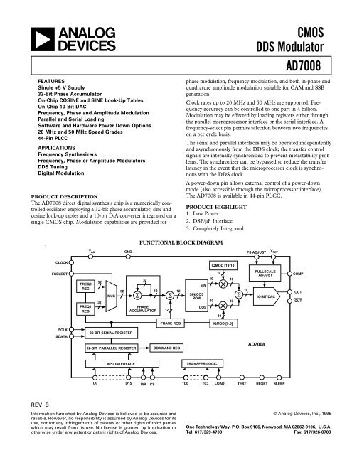
aFEATURESSingle +5 V Supply32-Bit Phase AccumulatorOn-Chip COSINE and SINE Look-Up TablesOn-Chip 10-Bit DACFrequency, Phase and Amplitude ModulationParallel and Serial LoadingSoftware and Hardware Power Down Options20 MHz and 50 MHz Speed Grades44-Pin PLCCAPPLICATIONSFrequency SynthesizersFrequency, Phase or Amplitude <strong>Modulator</strong>s<strong>DDS</strong> TuningDigital ModulationPRODUCT DESCRIPTIONThe <strong>AD7008</strong> direct digital synthesis chip is a numerically controlledoscillator employing a 32-bit phase accumulator, sine andcosine look-up tables and a 10-bit D/A converter integrated on asingle <strong>CMOS</strong> chip. Modulation capabilities are provided for<strong>CMOS</strong><strong>DDS</strong> <strong>Modulator</strong><strong>AD7008</strong>phase modulation, frequency modulation, and both in-phase andquadrature amplitude modulation suitable for QAM and SSBgeneration.Clock rates up to 20 MHz and 50 MHz are supported. Frequencyaccuracy can be controlled to one part in 4 billion.Modulation may be effected by loading registers either throughthe parallel microprocessor interface or the serial interface. Afrequency-select pin permits selection between two frequencieson a per cycle basis.The serial and parallel interfaces may be operated independentlyand asynchronously from the <strong>DDS</strong> clock; the transfer controlsignals are internally synchronized to prevent metastability problems.The synchronizer can be bypassed to reduce the transferlatency in the event that the microprocessor clock is synchronouswith the <strong>DDS</strong> clock.A power-down pin allows external control of a power-downmode (also accessible through the microprocessor interface)The <strong>AD7008</strong> is available in 44-pin PLCC.PRODUCT HIGHLIGHT1. Low Power2. DSP/µP Interface3. Completely IntegratedFUNCTIONAL BLOCK DIAGRAMGNDFS ADJUSTV REFCLOCKIQMOD [19:10]FSELECTFREQ0REGFREQ1REG3232MUX32Σ3212PHASEACCUMULATOR12Σ12SINSIN/COSROMCOS101010101010Σ10FULLSCALEADJUST10-BIT DACCOMPIOUTIOUTPHASE REGIQMOD [9:0]SCLKSDATA32-BIT SERIAL REGISTER32-BIT PARALLEL REGISTERCOMMAND REG<strong>AD7008</strong>MPU INTERFACETRANSFER LOGICD0V AAWR CSD15TC0 TC3 LOADTESTRESETSLEEPREV. BInformation furnished by Analog Devices is believed to be accurate andreliable. However, no responsibility is assumed by Analog Devices for itsuse, nor for any infringements of patents or other rights of third partieswhich may result from its use. No license is granted by implication orotherwise under any patent or patent rights of Analog Devices.© Analog Devices, Inc., 1995One Technology Way, P.O. Box 9106, Norwood. MA 02062-9106, U.S.A.Tel: 617/329-4700 Fax: 617/326-8703
<strong>AD7008</strong>–SPECIFICATIONS 1(V AA = V DD = +5 V ± 5%; T A = T MIN to T MAX , R SET = 390 Ω, R LOAD = 1 Ω forIOUT and IOUT, unless otherwise noted)<strong>AD7008</strong>AP20 <strong>AD7008</strong>JP50 Test Conditions/Parameter Min Typ Max Min Typ Max Units CommentsSIGNAL DAC SPECIFICATIONSResolution 10 10 BitsUpdate Rate (f MAX ) 20 50 MSPSIOUT Full Scale 20 20 mAOutput Compliance 1 1 VoltsDC AccuracyIntegral Nonlinearity +1 +1 LSBDifferential Nonlinearity ± 1 ± 1 LSB<strong>DDS</strong> SPECIFICATIONS 2Update Rate (f MAX ) 20 50 MSPSDynamic SpecificationsSignal-to-Noise 50 50 dB f CLK = f MAX ,f OUT = 2 MHzTotal Harmonic Distortion –55 –53 dB f CLK = f MAX ,f OUT = 2 MHzSpurious Free Dynamic Range (SFDR) 3Narrow Band (±50 kHz) –70 –70 dBc f CLK = 6.25 MHz,f OUT = 2.11 MHzWide Band (±2 MHz) –55 –55 dBcVOLTAGE REFERENCEInternal Reference @ +25°C 4 1.2 1.27 1.35 1.2 1.27 1.35 VoltsReference TC 300 300 ppm/°CV REF Overdrive 5 0 2 0 2 VLOGIC INPUTSV INH , Input High Voltage V DD –0.9 V DD –0.9 VoltsV INL , Input Low Voltage 0.9 0.9 VoltsI INH , Input Current 10 10 µAC IN , Input Capacitance 10 10 pFPOWER SUPPLIESV DD 4.75 5.25 4.75 5.25 VoltsI AA 26 26 mA R SET = 390 ΩI DD 22 + 1.5/MHz 22 + 1.5/MHz mAI AA + I DDf CLK = Max 80 110 125 160 mASleep = V DD 10 20 mANOTES1 Operating temperature ranges as follows: A Version: –40°C to +85°C; J Version: 0°C to +70°C.2 All dynamic specifications are measured using IOUT. 100% Production tested.3 f CLK = 6.25 MHz, Frequency Word = 5671C71C HEX, f OUT = 2.11 MHz.4 V REF may be externally driven between 0 and V DD .5 Do not allow reference current to cause power dissipation beyond the limit of I AA + I DD shown above.Specifications subject to change without notice.–2–REV. B
<strong>AD7008</strong>TIMING CHARACTERISTICS (V AA = V DD +5 V ± 5%; T A = T MIN to T MAX , unless otherwise noted)<strong>AD7008</strong>AP20<strong>AD7008</strong>JP50Parameter Min Typ Max Min Typ Max Units Test Conditions/Commentst 1 50 20 ns CLOCK Periodt 2 20 8 ns CLOCK High Durationt 3 20 8 ns CLOCK Low Durationt 4 5 5 ns CLOCK to Control Setup Timet 5 3 3 ns CLOCK to Control Hold Timet 6 4t 1 4t 1 ns LOAD Periodt 7 2t 1 2t 1 ns LOAD High Duration 1t 8 5 5 ns LOAD High to TC0–TC3 Setup Timet 9 5 5 ns LOAD High to TC0–TC3 Hold Timet 10 10 10 ns WR Falling to CS Low Setup Timet 11 10 10 ns WR Falling to CS Low Hold Timet 12 20 20 ns Minimum WR Low Durationt 13 10 10 ns Minimum WR High Durationt 14 3 3 ns WR to D0–D15 Setup Timet 15 3 3 ns WR to D0–D15 Hold Timet 16 20 20 ns SCLK Periodt 17 8 8 ns SCLK High Durationt 18 8 8 ns SCLK Low Durationt 19 10 10 ns SCLK Rising to SDATA Setup Timet 20 10 10 ns SCLK Rising to SDATA Hold TimeNOTE1 May be reduced to 1t 1 if LOAD is synchronized to CLOCK and Setup (t 4 ) and Hold (t 5 ) Times for LOAD to CLOCK are observed.t 1t 3CSCLOCKt 4t 5t 2WRt 10 t 11t 12 t 13FSEL, LOAD,TC3–TC0VALIDVALIDD0–D15t 14 t 15VALID DATAFigure 1. Clock Synchronization TimingFigure 3. Parallel Port TimingLOADt 6t 7t 8t 9SCLKt 20t 16t 17t 19t 18TC0–TC3VALIDSDATADB31DB0Figure 2. Register Transfer TimingFigure 4. Serial Port TimingREV. B –3–
<strong>AD7008</strong>ABSOLUTE MAXIMUM RATINGS*(T A = +25°C unless otherwise noted)V AA , V DD to GND . . . . . . . . . . . . . . . . . . . . . . . –0.3 V to +7 VAGND to DGND . . . . . . . . . . . . . . . . . . . . . –0.3 V to +0.3 VDigital I/O Voltage to DGND . . . . . . . . –0.3 V to V DD + 0.3 VAnalog I/O Voltage to AGND . . . . . . . . –0.3 V to V DD + 0.3 VOperating Temperature RangeIndustrial (A Version) . . . . . . . . . . . . . . . . . –40°C to +85°CCommercial (J Version) . . . . . . . . . . . . . . . . . .0°C to +70°CStorage Temperature Range . . . . . . . . . . . . . –65°C to +150°CLead Temperature (Soldering, 10 secs) . . . . . . . . . . . . +300°CJunction Temperature . . . . . . . . . . . . . . . . . . . . . . . . . +115°CPLCC θ JA Thermal Impedance . . . . . . . . . . . . . . . +53.8°C/Wθ JC Thermal Impedance . . . . . . . . . . . . . . . +24.1°C/W*Stresses above those listed under “Absolute Maximum Ratings” may causepermanent damage to the device. This is a stress rating only and functionaloperation of the device at these or any other conditions above those listed in theoperational sections of this specification is not implied. Exposure to absolutemaximum rating conditions for extended periods may affect device reliability.ORDERING GUIDETemperature Package PackageModel Range Description Option<strong>AD7008</strong>AP20 –40°C to +85°C 44-Pin PLCC P-44A<strong>AD7008</strong>JP50 0°C to +70°C 44-Pin PLCC P-44A<strong>AD7008</strong>/PCB*1–3.5" Disk32-BIT PARALLEL ASSEMBLY REGISTERMSBLSBA WORDD15–D0 ← A WORD*A WORDB WORDD15–D0 ← B WORD*MOST SIGNIFICANT WORD IS LOADED FIRSTFigure 5. 16-Bit Parallel Port Loading Sequence32-BIT PARALLEL ASSEMBLY REGISTERMSBLSBA BYTE D7–D0 ← A BYTE*A BYTE B BYTE D7–D0 ← B BYTEA BYTE B BYTE C BYTE D7–D0 ← C BYTEA BYTE B BYTE C BYTE D BYTE D7–D0 ← D BYTE*MOST SIGNIFICANT BYTE IS LOADED FIRSTFigure 6. 8-Bit Parallel Port Loading Sequence*<strong>AD7008</strong>/PCB <strong>DDS</strong> Evaluation Kit, assembled and tested. Kit includes an<strong>AD7008</strong>JP50.CAUTIONESD (electrostatic discharge) sensitive device. Electrostatic charges as high as 4000 V readilyaccumulate on the human body and test equipment and can discharge without detection.Although the <strong>AD7008</strong> features proprietary ESD protection circuitry, permanent damage mayoccur on devices subjected to high energy electrostatic discharges. Therefore, proper ESDprecautions are recommended to avoid performance degradation or loss of functionality.WARNING!ESD SENSITIVE DEVICEPIN CONFIGURATIONPLCCVREFCOMPFS ADJUSTVAAIOUTIOUTAGNDDGNDSDATASCLKTEST6 40DGNDD8D9D10D11D12D13D14D15WRV DD7 39PIN NO. 1 IDENTIFIER<strong>AD7008</strong> PLCCTOP VIEW(NOT TO SCALE)17 2918 28V DDRESETSLEEPLOADTC3TC2TC1TC0FSELECTCLOCKDGNDDGNDD0D1D2D3D4D5D6D7CSV DD–4–REV. B
<strong>AD7008</strong>MnemonicFunctionPIN DESCRIPTIONPOWER SUPPLYV AAPositive power supply for the analog section. A 0.1 µF decoupling capacitor should be connected between V AA andAGND. This is +5 V ± 5%.AGND Analog Ground.V DDPositive power supply for the digital section. A 0.1 µF decoupling capacitor should be connected between V DDand DGND. This is +5 V ± 5%. Both V AA and V DD should be externally tied together.DGND Digital Ground; both AGND and DGND should be externally tied together.ANALOG SIGNAL AND REFERENCEIOUT, IOUT Current Output. This is a high impedance current source. A load resistor should be connected between IOUTand AGND. IOUT should be either tied directly to AGND or through an external load resistor to AGND.FS ADJUST Full-Scale Adjust Control. A resistor (R SET ) is connected between this pin and AGND. This determines the magnitudeof the full-scale DAC current. The relationship between R SET and the full-scale current is as follows:IOUT FULL-SCALE (mA) =6233 ×V REFR SETV REF = 1.27 V nominal R SET = 390 Ω typicalV REF Voltage Reference Input. A 0.1 µF decoupling ceramic capacitor should be connected between V REF and V AA .There is an internal 1.27 volt reference which can be overdriven by an external reference if required. Seespecifications for maximum range.COMP Compensation pin. This is a compensation pin for the internal reference amplifier. A 0.1 µF decoupling ceramiccapacitor should be connected between COMP and V AA .DIGITAL INTERFACE AND CONTROLCLOCK Digital Clock Input for DAC and NCO. <strong>DDS</strong> output frequencies are expressed as a binary fraction of the frequencyof this clock. The output frequency accuracy and phase noise is determined by this clock.FSELECT Frequency Select Input. FSELECT controls which frequency register, FREQ0 or FREQ1, is used in the phaseaccumulator. Frequency selection can be done on a cycle-per-cycle basis. See Tables I, II and III.LOAD Register load, active high digital Input. This pin, in conjunction with TC3–TC0, control loading of internal registersfrom either the parallel or serial assembly registers. The load pin must be high at least 1t 1 . See Table II.TC3–TC0 Transfer Control address bus, digital inputs. This address determines the source and destination registers that areused during a transfer. The source register can either be the parallel assembly register or the serial assembly register.The destination register can be any of the following: COMMAND REG, FREQ0 REG, FREQ1 REG,PHASE REG or IQMOD REG. TC3–TC0 should be valid prior to LOAD rising and should not change untilLOAD falls. The Command Register can only be loaded from the parallel assembly register. See Table II.CSWRD7–D0D15–D8SCLKSDATASLEEPRESETTESTChip Select, active low digital input. This input in conjunction with WR is used when writing to the parallelassembly register.Write, active low digital input. This input in conjunction with CS is used when writing to the parallel assemblyregister.Data Bus, digital inputs. These represent the low byte of the 16-bit data input port used to write to the 32-bitparallel assembly register. The databus can configured for either a 8-bit or 16-bit MPU/DSP ports.Data Bus, digital inputs. These represent the high byte of the 16-bit data input port used to write to the 32-bitparallel assembly register. The databus can be configured for either a 8-bit or 16-bit MPU/DSP ports. When thedatabus is configured for 8-bit operation, D8–D15 should be tied to DGND.Serial Clock, digital input. SCLK is used, in conjunction with SDATA, to clock data into the 32-bit serial assemblyregister.Serial Data, digital input. Serial data is clocked on the rising edge of SCLK, Most Significant Bit (MSB) first.Low power sleep control, active high digital input. SLEEP puts the <strong>AD7008</strong> into a low power sleep mode. Internalclocks are disabled, while also turning off the DAC current sources. A SLEEP bit is also provided in theCOMMAND REG to put the <strong>AD7008</strong> into a low power sleep mode.Register Reset, active high digital input. RESET clears the COMMAND REG and all the modulation registers tozero.Test Mode. This is used for factory test only and should be left as a No Connect.REV. B –5–
<strong>AD7008</strong>14 PIPELINE DELAYS13 PIPELINE DELAYS11 PIPELINE DELAYS<strong>AD7008</strong>REGISTERANDCONTROLLOGIC321220PHASEACCUMULATOR3212PHASESUMMATION12ROMSINCOS1010SIN/COSSUMMATION9:0 19:10101010DACACCUM RESETSLEEPAM ENABLEIOUT/IOUTFigure 7. <strong>AD7008</strong> <strong>CMOS</strong> <strong>DDS</strong> <strong>Modulator</strong> (See Table I)SLEEP (37)SCLK (41)SDATA (42)D Qx 3232-BIT SERIALASSEMBLY REGISTERCOMMAND REGISTER31:003:0D2x 3231:0 D Q1x 4CLKDQAM ENABLED0-D15(19-26, 8-15)WR (16)CS (27)23:015:0 23:815:8 7:07:032-BIT PARALLELASSEMBLY REGISTER031:8x 241D Qx 32CLKREGISTERMUXD QCLKCLKD QD1D0D3BUS MODECLKSYNCHRO LOGICDQSLEEPLOAD (36)FSEL (31)TC0-TC3(32-35)D FLIP-FLOPS ARE MASTER SLAVE,LATCHING DATA ON CLK RISING EDGE.PASS FLIP-FLOPS ARE TRANSPARENTWHEN THE CLOCK IS LOW.TRANSFER CONTROL (TC) REGISTERD Qx 6PASSD Qx 6D Qx 6D Qx 60x 6D Q 1x 665TC0TC1TC3LOADTC3TRANSFER DECODE0011S223E 3x 54CLKFSELECTD Qx 540123FREQUENCYREGISTERSFREQ 032D Qx 32CLKE32CLKFREQ 1D Qx 32E1TO PHASEACCUMULATORCLKRESET SYNCHRONIZATIONTC2TC2CLKD QPHASE REGISTER12D Qx 12CLKE0x32TO PHASESUMMATIONRESET (38)CLKD Q D Q D QIQ MOD REGISTER10D Qx 20CLKETO SIN/COSSUMMATIONCLOCK (30)CLKACCUMULATORRESETFigure 8. <strong>AD7008</strong> Register and Control Logic–6–REV. B
<strong>AD7008</strong>Table I. Latency TableLatencyFunction (Synchronizer Enabled CR3 = 0 1 )FSelect 14t 1Phase 13t 1IQ Mod 11t 1NOTE1 All latencies are reduced by 4t 1 when CR3 = 1 (synchronizer disabled). 1t 1 isequal to one pipeline delay.Table II. Source and Destination RegisterTC3 TC2 TC1 TC0 LOAD Source Register Destination RegisterX X X X 0 N/A N/A0 0 X X 1 Parallel COMMAND*1 0 0 0 1 Parallel FREQ01 0 0 1 1 Parallel FREQ11 0 1 0 1 Parallel PHASE1 0 1 1 1 Parallel IQMOD1 1 0 0 1 Serial FREQ01 1 0 1 1 Serial FREQ11 1 1 0 1 Serial PHASE1 1 1 1 1 Serial IQMOD*The Command Register can only be loaded from the parallel assembly registers.Table III. <strong>AD7008</strong> Control RegistersRegister Size Reset State DescriptionCOMMAND REG* 4 Bits CR3–CR0 All Zeros Command Register. This is written to using the parallel assembly register.FREQ0 REG 32 Bits DB31–DB0 All Zeros Frequency Register 0. This defines the output frequency, whenFSELECT = 0, as a fraction of the CLOCK frequency.FREQ1 REG 32 Bits DB31–DB0 All Zeros Frequency Register 1. This defines the output frequency, whenFSELECT = 1, as a fraction of the CLOCK frequency.PHASE REG 12 Bits DB11–DB0 All Zeros Phase Offset Register. The contents of this register is added to theoutput of the phase accumulator.IQMOD REG 20 Bits DB19–DB0 All Zeros I and Q Amplitude Modulation Register. This defines the amplitude ofthe I and Q signals as 10-bit twos complement binary fractions.DB[19:10] is multiplied by the Quadrature (sine component andmultiplied by the In-Phase (cosine) component.*On power up, the Command Register should be configured by the user for the desired mode before operation.Table IV. Command Register Bits*CR0 = 0 Eight-Bit Databus. Pins D15–D8 are ignored and the parallel assembly register shifts eight places left on each write.Hence four successive writes are required to load the 32-bit parallel assembly register, Figure 6.= 1 Sixteen-Bit Databus. The parallel assembly register shifts 16 places left on each write. Hence two successive writes arerequired to load the 32-bit parallel assembly register, Figure 5.CR1 = 0 Normal Operation.= 1 Low Power Sleep Mode. Internal Clocks and the DAC current sources are turned off.CR2 = 0 Amplitude Modulation Bypass. The output of the sine LUT is directly sent to the DAC.= 1 Amplitude Modulation Enable. IQ modulation is enabled allowing AM or QAM to be performed.CR3 = 0 Synchronizer Logic Enabled. The FSELECT, LOAD and TC3–TC0 signals are passed through a 4-stage pipelineto synchronize them with the CLOCK, avoiding metastability problems.= 1 Synchronizer Logic Disabled. The FSELECT, LOAD and TC3–TC0 signals bypass the synchronization logic. Thisallows for faster response to the control signals.*The Command Register can only be loaded from the parallel assembly register.REV. B –7–
<strong>AD7008</strong>CIRCUIT DESCRIPTIONThe <strong>AD7008</strong> provides an exciting new level of integration forthe RF/Communications system designer. The <strong>AD7008</strong> combinesthe numerically controlled oscillator (NCO), SINE/CO-SINE look-up tables, frequency, phase and IQ modulators, anda digital-to-analog converter on a single integrated circuit.The internal circuitry of the <strong>AD7008</strong> consists of four main sections.These are:Numerically Controlled Oscillator (NCO) + Phase <strong>Modulator</strong>SINE and COSINE Look-Up TablesIn Phase and Quadrature <strong>Modulator</strong>sDigital-to-Analog ConverterThe <strong>AD7008</strong> is a fully integrated Direct Digital Synthesis(<strong>DDS</strong>) chip. The chip requires one reference clock, two lowprecisionresistors and six decoupling capacitors to providedigitally created sine waves up to 25 MHz. In addition to thegeneration of this RF signal, the chip is fully capable of a broadrange of simple and complex modulation schemes. Thesemodulation schemes are fully implemented in the digital domainallowing accurate and simple realization of complex modulationalgorithms using DSP techniques.THEORY OF OPERATIONSine waves are typically thought of in terms of their amplitudeform: a(t) = sin (ωt) or a(t) = cos (ωt). However, these are nonlinearand not easy to generate except through piece wise construction.On the other hand, the angular information is linearin nature. That is, the phase angle rotates though a fixed anglefor each unit of time. The angular rate depends on the frequencyof the signal by the traditional rate of: ω = 2 πf.+10–12π0MAGNITUDEPHASEFigure 9.Knowing that the phase of a sine wave is linear and given a referenceinterval (clock period), the phase rotation for that periodcan be determined.Solving for w:∆Phase =ωdtω= ∆Phasedt= 2 πfSolving for f and substituting the reference clock frequency for⎛the reference period: ⎜⎝1f CLOCK⎞= dt⎟:⎠The <strong>AD7008</strong> builds the output based on this simple equation.A simple <strong>DDS</strong> chip will implement this equation with 3 majorsubcircuits. The <strong>AD7008</strong> has an extra section for I and Qmodulation.Numerically Controlled Oscillator + Phase <strong>Modulator</strong>This consists of two frequency select registers, a phase accumulatorand a phase offset register. The main component of theNCO is a 32-bit phase accumulator which assembles the phasecomponent of the output signal. Continuous time signals have aphase range 0 to 2 π. Outside this range of numbers, the sinusoidalfunctions repeat themselves in a periodic manner. Thedigital implementation is no different. The accumulator simplyscales the range of phase numbers into a multibit digital word.The phase accumulator in the <strong>AD7008</strong> is implemented with 32bits. Therefore in the <strong>AD7008</strong>, 2 π = 2 32 . Likewise, the ∆Phaseterm is scaled into this range of numbers 0 ≤ ∆Phase ≤ 2 32 – 1.Making these substitutions into the equation above:f = ∆Phase × f CLOCK2 32 where 0 ≤∆Phase < 2 32With a clock signal of 50 MHz and a phase word of 051EB852hex:f =51EB852 × 50 MHz2 32 = 1.000000000931 MHzThe input to the phase accumulator (i.e., the phase step) can beselected either from the FREQ0 Register or FREQ1 Register,and this is controlled by the FSELECT pin. The phase accumulatorin the <strong>AD7008</strong> inherently generates a continuous 32-bit phase signal, thus avoiding any output discontinuity whenswitching between frequencies. This facilitates complex frequencymodulation schemes, such as GMSK.Following the NCO, a phase offset can be added to performphase modulation using the 12-bit PHASE Register. The contentsof this register are added to the most significant bits of theNCO.Sine and Cosine Look-Up TablesTo make the output useful, the signal must be converted fromphase information into a sinusoidal value. Since phase informationmaps directly into amplitude, a ROM look up table convertsthe phase information into amplitude. To do this thedigital phase information is used to address a Sine/Cosine ROMLUT. Only the most significant 12 bits are used for this purpose.The remaining 20 bits provide frequency resolution andminimize the effects of quantization of the phase to amplitudeconversion.In Phase and Quadrature <strong>Modulator</strong>sTwo 10-bit amplitude multipliers are provided allowing the easyimplementation of either Quadrature Amplitude Modulation(QAM) or Amplitude Modulation (AM). The 20-bit IQMODRegister is used to control the amplitude of the I (cos) and Q(sin) signals. IQMOD [9:0] controls the I amplitude andIQMOD [19:10] controls the Q amplitude.The user should ensure that when summing the I and Q signalsthe sum should not exceed the value that a 10-bit accumulatorcan hold. The <strong>AD7008</strong> does not clip the digital output; theoutput will roll over instead of clip.f = ∆Phase × f CLOCK2 π–8–REV. B
<strong>AD7008</strong>When amplitude modulation is not required, the IQ multiplierscan be bypassed (CR = 2). The sine output is directly sent tothe 10-bit DAC.Digital-to-Analog ConverterThe <strong>AD7008</strong> includes a high impedance current source 10-bitDAC, capable of driving a wide range of loads at differentspeeds. Full-scale output current can be adjusted, for optimumpower and external load requirements, through the use of asingle external resistor (R SET ).The DAC can be configured for single or differential-endedoperation. IOUT can be tied directly to AGND for single-endedoperation or through a load resistor to develop an output voltage.The load resistor can be any value required as long as thefull-scale voltage developed across it does not exceed 1 volt.Since full-scale current is controlled by R SET , adjustments toR SET can balance changes made to the load resistor.DSP and MPU InterfacingThe <strong>AD7008</strong> contains a 32-bit parallel assembly register and a32-bit serial assembly register. Each of the modulation registerscan be loaded from either assembly register under control of theLOAD pin and the Transfer-Control (TC) pins (See Table II).The Command register can be loaded only from the parallel assemblyregister. In practical use, both serial and parallel interfacescan be used simultaneously if the application requires.TC3–TC0 should be stable before the LOAD signal rises andshould not change until after LOAD falls (Figure 2).The DSP/MPU asserts both WR and CS to load the parallel assemblyregister (Figure 3). At the end of each write, the parallelassembly register is shifted left by 8 or 16 bits (Depending onCR0), and the new data is loaded into the low bits. Hence, two16-bit writes or four 8-bit writes are used to load the parallel assemblyregister. When loading parallel data, it is only necessaryto write as much data as will be used by that register. For instance,the Command Register requires only one write to theparallel assembly register.Serial data is input to the chip on the rising edge of SCLK, mostsignificant bit first (Figure 4). The data in the assembly registerscan be transferred to the modulation registers by means ofthe transfer control pins.Maximum Updating of the <strong>AD7008</strong>Updating the <strong>AD7008</strong> need not take place in a synchronousfashion. However, in asynchronous systems, most of the externalclock pulses (LOAD and SCLK) must be high for greaterthan one system clock period. This insures that at least oneCLOCK rising edge will occur successfully completing the latchfunction (Figure 1).However, if the <strong>AD7008</strong> is run in a synchronous mode with thecontrolling DSP or microcontroller, the <strong>AD7008</strong> may be loadedvery rapidly. Optimal speed is attained when operated in the16-bit load mode; the following discussion will assume thatmode is used. Each of the modulation registers require two 16bit loads. This data is latched into the parallel assembly registeron the falling edge of the WR command. This strobe is notqualified by the CLOCK pulse but must be held low for a minimumof 20 ns and only need be high for 10 ns. The two 16-bitwords may be loaded in succession. While the second 16-bitword is being latched into the parallel assembly register, theTransfer and Control word may be presented to the TC3–TC0pins. If the designation register is always the same, an externalregister can be used to store the information on the inputs ofTC3–TC0. At some time after the second falling edge of WR,the LOAD signal may go high. As long as the load signal is high5 ns (see setup time) before the rising edge of the CLOCK signal,data will be transferred to the destination register.The limiting factor of this technique is the WR period which is30 ns. Thus the CLOCK may run up to 33 MSPS using thistechnique and the effective update rate would be one half or16.5 MHz. See timing Figure 10 for timing details.DATAWRCLOCKTCLOADHI WORDLOW WORDFigure 10. Accelerated Data Load SequenceAPPLICATIONSSerial ConfigurationData is written to the <strong>AD7008</strong> in serial mode using the two signallines SDATA and SCLK. Data is accumulated in the serialassembly register with the most significant bit loaded first. Thedata bits are loaded on the rising edge of the serial clock. Oncedata is loaded in the serial assembly register, it must be transferredto the appropriate register on chip. This is accomplishedby setting the TC bits according to Tables II and III. If youwant to load the serial assembly register into FREQ1 register,the TC bits should be 1101. When the LOAD pin is raised,data is transferred directly to the FREQ1 register. When operatingin serial mode, some functions must still operate in parallelmode such as loading the TC bits and updating the Commandregister which is accessed only through the parallel assemblyregister. See Figure 11 for a typical serial mode configuration.+5VU21450MHzV CC8OUTV EE7K1115WRLOADSCLKSDATARESETCMD0CMD1CMD2CMD3TC0TC1TC2TC319202122232425268910111213141516273233343536414231303837D0D1D2D3D4D5D6D7D8D9D10D11D12D13D14D15WRU3<strong>AD7008</strong>CSTC0TC1TC2TC3LOADSCLKSDATAFSELECTCLKRESETSLEEPC16V REF+5V0.1µF C25+5VCOMP0.1µF2 R4IOUT149.9R3IOUT49.9FSADJUSTV AAV DDV DDV DDAGNDDGNDDGNDDGNDDGNDTEST4317283944718294340R5390+5V+5V+5V+5VFigure 11. General Purpose Serial InterfaceREV. B –9–
<strong>AD7008</strong>–Typical Performance CharacteristicsREF 5.0 dBm10 dB/DIV RANGE 5.0 dBmOFFSET 4 640 000.0 Hz–54.8 dBCOMPV REFV REF6115Ω+5V5TO DAC<strong>AD7008</strong>4R SETSTART 0 HzRBW 3 kHzVBW 10 kHzSTOP 10 000 000.0 HzST 2.4 SECFigure 17. Equivalent Reference CircuitFigure 20. f CLK = 20 MHz, f OUT = 5.1 MHzREF 4.3 dBm10 dB/DIV RANGE 5.0 dBmOFFSET 3 330 000.0 Hz–63.6 dBREF 4.3 dBm10 dB/DIV RANGE 5.0 dBmOFFSET 6 320 000.0 Hz–61.3 dBSTART 0 HzRBW 3 kHzVBW 10 kHzSTOP 10 000 000.0 HzST 2.4 SECSTART 0 HzRBW 3 kHzVBW 10 kHzSTOP 10 000 000.0 HzST 2.4 SECFigure 18. f CLK = 20 MHz, f OUT = 1.1 MHzFigure 21. f CLK = 20 MHz, f OUT = 2.1 MHzREF 4.3 dBm10 dB/DIV RANGE 5.0 dBmOFFSET 4 500 000.0 Hz–61.1 dBREF 5.0 dBm10 dB/DIV RANGE 5.0 dBmOFFSET –490 000.0 Hz–63.4 dBSTART 0 HzRBW 3 kHzVBW 10 kHzSTOP 10 000 000.0 HzST 2.4 SECSTART 0 HzRBW 3 kHzVBW 10 kHzSTOP 10 000 000.0 HzST 2.4 SECFigure 19. f CLK = 20 MHz, f OUT = 3.1 MHzFigure 22. f CLK = 20 MHz, f OUT = 4.1 MHz–12–REV. B
Typical Performance Characteristics–<strong>AD7008</strong>REF 5.0 dBm10 dB/DIV RANGE 5.0 dBmOFFSET 1 680 000.0 Hz–52.8 dBREF 4.3 dBm10 dB/DIV RANGE 5.0 dBmOFFSET 14 500 000.0 Hz–52.4 dBSTART 0 HzRBW 3 kHzVBW 10 kHzSTOP 10 000 000.0 HzST 2.4 SECFigure 23. f CLK = 20 MHz, f OUT = 6.1 MHzCENTER 16 000 000.0 HzRBW 3 kHzVBW 10 kHzSPAN 25 000 000.0 HzST 5.6 SECFigure 26. f CLK = 50 MHz, f OUT = 7.1 MHzREF 4.3 dBm10 dB/DIV RANGE 5.0 dBmOFFSET 500 000.0 Hz–51.7 dBREF 5.0 dBm10 dB/DIV RANGE 5.0 dBmOFFSET –1 280 000.0 Hz–51.8 dBCENTER 6 500 000.0 HzRBW 3 kHzVBW 10 kHzSPAN 10 000 000.0 HzST 2.4 SECSTART 0 HzRBW 3 kHzVBW 10 kHzSTOP 10 000 000.0 HzST 2.4 SECFigure 24. f CLK = 20 MHz, f OUT = 6.5 MHzFigure 27. f CLK = 20 MHz, f OUT = 7.1 MHzREF 4.3 dBm10 dB/DIV RANGE 5.0 dBmOFFSET 6 304 000.0Hz–56.3 dBREF 4.3 dBm10 dB/DIV RANGE 5.0 dBmOFFSET 15 300 000.0 Hz–51.8 dBSTART 0 HzRBW 3 kHzVBW 10 kHzSTOP 16 000 000.0 HzST 3.6 SECSTART 0 HzRBW 3 kHzVBW 10 kHzSTOP 25 000 000.0 HzST 5.6 SECFigure 25. f CLK = 50 MHz, f OUT = 2.1 MHzFigure 28. f CLK = 50 MHz, f OUT = 5.1 MHzREV. B –13–
<strong>AD7008</strong>–Typical Performance CharacteristicsREF 5.0 dBm10 dB/DIV RANGE 5.0 dBmOFFSET 4 500 000.0 Hz–54.7 dBREF 5.0 dBm10 dB/DIV RANGE 5.0 dBmOFFSET 500 000.0 Hz–44.8 dBSTART 0 HzRBW 3 kHzVBW 10 kHzSTOP 25 000 000.0 HzST 5.6 SECCENTER 16 500 000.0 HzRBW 3 kHzVBW 10 kHzSPAN 25 000 000.0 HzST 5.6 SECFigure 29. f CLK = 50 MHz, f OUT = 9.1 MHzFigure 32. f CLK = 50 MHz, f OUT = 16.5 MHzREF 5.0 dBm10 dB/DIV RANGE 5.0 dBmOFFSET 11 100 000.0 Hz–54.1 dB130120TOTAL CURRENT I AA+ I DD– mA11010090807060START 0 HzRBW 3 kHzVBW 10 kHzSTOP 25 000 000.0 HzST 5.6 SECFigure 30. f CLK = 50 MHz, f OUT = 11.1 MHz50010 20 30 40 50MASTER CLOCK – MHzFigure 33. Typical Current Consumption vs. FrequencyREF 5.0 dBm10 dB/DIV RANGE 5.0 dBmOFFSET 10 675 000.0 Hz–47.0 dB–40–45WIDEBAND SFDR – dB–50–55–60–65–70CENTER 13 100 000.0 HzRBW 3 kHzVBW 10 kHzSPAN 25 000 000.0 HzST 5.6 SEC–750102030MASTER CLOCK – MHz4050Figure 31. f CLK = 50 MHz, f OUT = 13.1 MHzFigure 34. Typical Plot of SFDR vs. Master Clock FrequencyWhen f OUT = 1/3f CLK , Frequency Word = 5671C71C Hex–14–REV. B
<strong>AD7008</strong><strong>AD7008</strong>/PCB <strong>DDS</strong> EVALUATION BOARDThe <strong>AD7008</strong>/PCB <strong>DDS</strong> Evaluation Board allows designers toevaluate the high performance <strong>AD7008</strong> <strong>DDS</strong> <strong>Modulator</strong> with aminimum amount of effort.To prove this <strong>DDS</strong> will meet the user’s waveform synthesis requirements,the only things needed are the <strong>AD7008</strong>/PCB <strong>DDS</strong>Evaluation Board, +5 V power supply, an IBM-compatible PC,and a spectrum analyzer. The evaluation setup is shown below.The <strong>DDS</strong> evaluation kit includes a populated, tested <strong>AD7008</strong>/PCB board; software which controls the <strong>AD7008</strong> through theparallel printer port in a DOS or Windows environment and an<strong>AD7008</strong>P.The <strong>AD7008</strong> direct digital synthesis chip is a numericallycontrolled oscillator employing a 32-bit phase accumulator, sineand cosine look-up tables, and a l0-bit D/A converter integratedon a single <strong>CMOS</strong> chip. Modulation capabilities are providedfor phase modulation, frequency modulation, and both in-phaseand quadrature amplitude modulation suitable for SSBgeneration.Clock rates up to 20 MHz and 50 MHz are supported. Frequencyaccuracy can be controlled to one part in four billion.OPTIONALTTL CLOCKREFERENCEGENERATORSTANDARDPRINTERCABLESOFTWAREPROVIDEDCLOCKOSCILLATORINTERFACELOGICIBM-COMPATIBLE PC<strong>AD7008</strong>50MHz<strong>CMOS</strong> <strong>DDS</strong>POWERSUPPLYINTERFACE<strong>AD7008</strong> <strong>DDS</strong> EVALUATION BOARD50Ω CABLESPECTRUM ANALYZEREXTERNALPOWERSUPPLYFigure 35. <strong>AD7008</strong> <strong>DDS</strong> Evaluation Board SetupTable IV. <strong>AD7008</strong>/PCB Typical Electrical Characteristics(Nominal power supplies, CLK = 50 MHz)TypicalCharacteristics Value Units+5.0 V Supply Current 125 mA<strong>AD7008</strong> Output Voltage 0 to +1.0 V(Terminated into 50 Ω Externally)<strong>CMOS</strong> clock input HIGH 4.1 to 5 V<strong>CMOS</strong> clock input LOW 0.0 to 0.5 VUSING THE <strong>AD7008</strong>/PCB <strong>DDS</strong> EVALUATION BOARDThe <strong>AD7008</strong>/PCB evaluation kit is a test system designed tosimplify the evaluation of the <strong>AD7008</strong> 50 MHz Direct DigitalSynthesizer. Provisions to control the <strong>AD7008</strong> from the printerport of an IBM-compatible PC are included, along with the+5Vnecessary software. This data sheet provides information onoperating the evaluation board; additional details are availablefrom the ADI technical assistance line 1-800-ANALOGD.Prototyping AreaAn area near one edge of the board is intentionally left void ofcomponents to allow the user to add additional circuits to theevaluation test set. Users may want to build custom analog filtersfor the outputs, or add buffers and operational amplifiersused in the final applications.XO vs. External ClockThe reference clock of the <strong>AD7008</strong>/PCB is normally providedby a 50 MHz <strong>CMOS</strong> oscillator. This oscillator can be removedand an external <strong>CMOS</strong> clock connected to CLOCK. If an externalclock is used, a 50 Ω resistor R6 should be installed.Power SupplyPower for the <strong>AD7008</strong>/PCB must be provided externallythrough the pin connections, as described in the Inputs/Outputs.The power leads should be twisted to reduce ground loops.<strong>AD7008</strong>/PCB BILL OF MATERIALQuantity Reference Description1 C1 Tag – Tant Cap, 10 µF, 35 V, 20%8 C2–C9 Cer Chip Cap, 0.1 µF, MurataGrm426 CLOCK, FSEL SMB – Submin Snap-on (Male)I OUT , I OUTN PCB MT PlugSCLK, SDATA1 FSADJ RN55 – Res Met Film, 3921 LK1 HDR SIP 3-Pin Male1 Shunt 530153-21 P1 36-Pin D Conn Rt Ang PcmtFem AMP1 P2 PC Voltage Ter Blk w/ScrewsAugat RDI3 R1–R3 RN55 – Res Met Film, 10k2 R4, R5 RN55 – Res Met Film, 49.91 RZ1 10P Bussed Res Ntwk, 10kCSC10A01103G1 RZ2 6P Bussed Res Ntwk, 4.7kCSC06A01472G1 U1 <strong>AD7008</strong> JP50 <strong>CMOS</strong> <strong>DDS</strong><strong>Modulator</strong>1 U2 74HC74 – Dual D-type Pos-Ed-Trigd Flip-Flop1 V REF Pin Terminal, Testpoint1 XTAL OSC XTAL, Fox F1100H50 MHz1 Socket, Methode 213-044-5014 Support, Nylon1 PCB, 48295(-)26 Pin Sockets, Closed EndREV. B –15–
<strong>AD7008</strong>Controlling the <strong>AD7008</strong>/PCBThe <strong>AD7008</strong>/PCB is designed to allow control (frequencyspecification, reset, etc.) through the parallel printer port of astandard IBM-compatible PC. The user simply disconnects theprinter cable from the printer and inserts it into edge connectorP1 of the evaluation board.The printer port provides information to the <strong>AD7008</strong>/PCBthrough eight data lines and four control lines. Control signalsare latched on the <strong>AD7008</strong>/PCB to prevent problems with longprinter cables.NameC36DRPFP1123456789101112131415161718192021222324252627282930313233343536LATCHD0D1D2D3D4D5D6D7RESETLOADWRD0D1D2D3D4D5D6D72345678910LATCHRESETLOADWR10k10PB+5RZ14.7k6PB+5RZ223456INPUTS/OUTPUTSDescriptionSMBFSELECTSMBCLKSMBSDATAXTAL114V CC8OUTV EEP136-pin edge connector to connect to parallelport of PC.CLOCK <strong>CMOS</strong> input for clock R6 provides termination.FSEL <strong>CMOS</strong> input to select between Freq 0 and Freq 1.Low selects Freq 0.SDATA <strong>CMOS</strong> input for serial input pin.SCLK <strong>CMOS</strong> input for clocking in SDATA.I OUTAnalog output.I OUT N Complementary analog output.V REFTest point for V REF pin.P2+5 V and ground power connection.LK1External sleep command input.R310k+5VC90.1µFSMBSCLKR650OPTIONALR210k7R110kD0D1D2D3D4D5D6D7LWRD0D1D2D3LLOADH3MLK1RESET123+5VGND19202122232425268910111213141516273233343536414231303837D0D1D2D3D4D5D6D7D8D9D10D11D12D13D14D15WRCSTC0TC1TC2TC3LOADRESETSLEEPFigure 36.A 3.5" floppy disk containing software to control the <strong>AD7008</strong> isprovided with the <strong>AD7008</strong>/PCB. This software was developedusing C. The C source code is provided in a file namedA:\<strong>AD7008</strong>.C, which the user may view, run, or modify.An executable version of this software is also provided, and canbe executed from DOS by typing “A:\<strong>AD7008</strong>.” The softwareprompts the user to provide the necessary information neededby the program. Additional information is included in a test filenamed A:\readme.txt.A windows 3.1 executable called WIN7008 is also included.U1DUT7008PSCLKSDATAFSELECTCLKV REFCOMPAGNDDGNDDGNDDGNDDGNDTEST653172839447182943400.048 (1.21)0.042 (1.07)0.020(0.50)R+5V+5V+5V+5V+5V U2474HC74PRLOAD 2 5D Q LLOAD3> CCLQ61+5V+5V10 U274HC7412 PR 9WR D Q L11WRLATCH> CCLQ813+5VOUTLINE DIMENSIONSDimensions shown in inches and (mm).44-Pin PLCC (P-44A)671718C70.1µFV REFC6R40.1µF50+5VI OUTI OUT21SMBR5I OUT504FSADJFSADJUST390+5VDV AAV DDV DDV DD0.048 (1.21)0.042 (1.07)PIN 1IDENTIFIERTOP VIEW(PINS DOWN)0.656 (16.66)0.650 (16.51) SQ0.695 (17.65)0.685 (17.40) SQP2PCTB2120.056 (1.42)0.042 (1.07)40392928C20.1µFSMBI OUTC30.1µF0.180 (4.57)0.165 (4.19)C40.1µFC110µF0.110 (2.79)0.085 (2.16)0.025 (0.63)0.015 (0.38)0.050(1.27)BSCC50.1µFC80.1µF0.021 (0.53)0.013 (0.33)0.032 (0.81)0.026 (0.66)0.040 (1.01)0.025 (0.64)+5V0.63 (16.00)0.59 (14.99)PRINTED IN U.S.A. C1791a–10–2/95–16–REV. B