Download HSP45102 12 Bit NCO Data Sheet
Download HSP45102 12 Bit NCO Data Sheet
Download HSP45102 12 Bit NCO Data Sheet

You also want an ePaper? Increase the reach of your titles
YUMPU automatically turns print PDFs into web optimized ePapers that Google loves.
SEMICONDUCTOR<br />
<strong>HSP45102</strong><br />
December 1996<br />
Features<br />
• 33MHz, 40MHz Versions<br />
• 32-<strong>Bit</strong> Frequency Control<br />
• BFSK, QPSK Modulation<br />
• Serial Frequency Load<br />
• <strong>12</strong>-<strong>Bit</strong> Sine Output<br />
• Offset Binary Output Format<br />
• 0.009Hz Tuning Resolution at 40MHz<br />
• Spurious Frequency Components
<strong>HSP45102</strong><br />
Pinout<br />
28 LEAD PDIP, 28 LEAD SOIC<br />
TOP VIEW<br />
OUT6 1<br />
OUT7 2<br />
OUT8 3<br />
OUT9 4<br />
OUT10 5<br />
OUT11 6<br />
GND 7<br />
V CC 8<br />
SEL_L/M 9<br />
SFTEN 10<br />
MSB/LSB 11<br />
ENPHAC <strong>12</strong><br />
SD 13<br />
SCLK 14<br />
28<br />
27<br />
26<br />
25<br />
24<br />
23<br />
22<br />
21<br />
20<br />
19<br />
18<br />
17<br />
16<br />
15<br />
OUT5<br />
OUT4<br />
OUT3<br />
OUT2<br />
OUT1<br />
OUT0<br />
V CC<br />
GND<br />
P0<br />
P1<br />
LOAD<br />
TXFR<br />
CLK<br />
GND<br />
Pin Description<br />
NAME TYPE DESCRIPTION<br />
V CC<br />
GND<br />
+5V power supply pin.<br />
Ground<br />
P0-1 I Phase modulation inputs (become active after a pipeline delay of four clocks). A phase shift of 0,<br />
90, 180, or 270 degrees can be selected as shown in Table 1.<br />
CLK I <strong>NCO</strong> clock. (CMOS level)<br />
SCLK I This pin clocks the frequency control shift register.<br />
SEL_L/M I A high on this input selects the least significant 32 bits of the 64-bit frequency register as the input<br />
to the phase accumulator; a low selects the most significant 32 bits.<br />
SFTEN I The active low input enables the shifting of the frequency register.<br />
MSB/LSB I This input selects the shift direction of the frequency register. A low on this input shifts in the data<br />
LSB first; a high shifts in the data MSB first.<br />
ENPHAC I This pin, when low, enables the clocking of the Phase Accumulator. This input has a pipeline delay<br />
of four clocks.<br />
SD I <strong>Data</strong> on this pin is shifted into the frequency register by the rising edge of SCLK when SFTEN<br />
is low.<br />
TXFR I This active low input is clocked onto the chip by CLK and becomes active after a pipeline delay of<br />
four clocks. When low, the frequency control word selected by SEL_L/M is transferred from the<br />
frequency register to the phase accumulator’s input register.<br />
LOAD I This input becomes active after a pipeline delay of five clocks. When low, the feedback in the<br />
phase accumulator is zeroed.<br />
OUT0-11 O Output data. OUT0 is LSB. Unsigned.<br />
All inputs are TTL level, with the exception of CLK.<br />
overline designates active low signals.<br />
5-48
<strong>HSP45102</strong><br />
P0-1<br />
ENPHAC<br />
TXFR<br />
LOAD<br />
CLK<br />
4-DLY<br />
R<br />
E<br />
G<br />
R.P0-1<br />
R.ENPHAC<br />
R.TXFR<br />
CLK<br />
R<br />
E<br />
G<br />
R.LOAD<br />
PHASE OFFSET ADDER<br />
R.P0-1<br />
13 MSBs<br />
/<br />
A<br />
D<br />
D<br />
E<br />
R<br />
/ 13<br />
CLK<br />
‘0’<br />
R<br />
E<br />
G<br />
/ 32<br />
/ 32<br />
/ 13 R<br />
E<br />
G<br />
M<br />
U<br />
X<br />
/ 32<br />
SINE<br />
ROM / <strong>12</strong><br />
CLK<br />
2-DLY<br />
R<br />
E<br />
G<br />
OUT0-11<br />
SD<br />
SCLK<br />
SFTEN<br />
MSB/LSB<br />
SEL_L/M<br />
FREQUENCY<br />
CONTROL<br />
SECTION<br />
64-BIT<br />
SHIFT<br />
REG<br />
R.LOAD<br />
ACCUMULATOR<br />
INPUT<br />
FRCTRL<br />
REGISTER<br />
/ 32 0-31<br />
M / 32 R<br />
U<br />
E<br />
/ 32 FRCTRL<br />
32-63<br />
/ 32<br />
X<br />
R.TXFR<br />
G<br />
/ 32<br />
R / 32<br />
R.ENPHAC E<br />
G<br />
CLK<br />
(HIGH SELECTS FRCTRL0-31, LOW SELECTS FRCTRL32-63)<br />
PHASE ACCUMULATOR<br />
A<br />
D<br />
D<br />
E<br />
R<br />
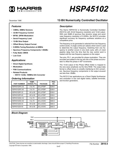
FIGURE 1. <strong>NCO</strong>-<strong>12</strong> FUNCTIONAL BLOCK DIAGRAM<br />
Functional Description<br />
The <strong>NCO</strong><strong>12</strong> produces a <strong>12</strong>-bit sinusoid whose frequency<br />
and phase are digitally controlled. The frequency of the sine<br />
wave is determined by one of two 32-bit words. Selection of<br />
the active word is made by SEL_L/M. The phase of the output<br />
is controlled by the two-bit input P0-1, which is used to<br />
select a phase offset of 0, 90, 180, or 270 degrees.<br />
As shown in the Block Diagram, the <strong>NCO</strong><strong>12</strong> consists of a<br />
Frequency Control Section, a Phase Accumulator, a Phase<br />
Offset Adder and a Sine ROM. The Frequency Control section<br />
serially loads the frequency control word into the frequency<br />
register. The Phase Accumulator and Phase Offset<br />
Adder compute the phase angle using the frequency control<br />
word and the two phase modulation inputs. The Sine ROM<br />
generates the sine of the computed phase angle. The format<br />
of the <strong>12</strong>-bit output is offset binary.<br />
Frequency Control Section<br />
The Frequency Control Section shown in Figure 1 serially<br />
loads the frequency data into a 64-bit, bidirectional shift register.<br />
The shift direction is selected with the MSB/LSB input.<br />
When this input is high, the frequency control word on the<br />
SD input is shifted into the register MSB first. When<br />
MSB/LSB is low the data is shifted in LSB first. The register<br />
shifts on the rising edge of SCLK when SFTEN is low. The<br />
timing of these signals is shown in Figures 2A and 2B.<br />
The 64 bits of the frequency register are sent to the Phase<br />
Accumulator Section where 32 bits are selected to control<br />
the frequency of the sinusoidal output.<br />
Phase Accumulator Section<br />
The phase accumulator and phase offset adder compute the<br />
phase of the sine wave from the frequency control word and<br />
the phase modulation bits P0-1. The architecture is shown in<br />
Figure 1. The most significant 13 bits of the 32-bit phase<br />
accumulator are summed with the two-bit phase offset to<br />
generate the 13-bit phase input to the Sine Rom. A value of<br />
0 corresponds to 0 o , a value of 1000 hexadecimal corresponds<br />
to a value of 180 o .<br />
The phase accumulator advances the phase by the amount<br />
programmed into the frequency control register. The output<br />
frequency is equal to:<br />
F LO<br />
= ( N× F CLK<br />
⁄ 2 32 ), or<br />
(EQ. 1)<br />
⎛<br />
N INT F OUT⎞ 32 = ⎜--------------<br />
⎟ 2 ,<br />
(EQ. 2)<br />
⎝F CLK ⎠<br />
where N is the 32 bits of frequency control word that is programmed.<br />
INT[•] is the integer of the computation. For example,<br />
if the control word is 20000000 hexadecimal and the clock<br />
frequency is 30MHz, then the output frequency would be<br />
F CLK /8, or 3.75MHz.<br />
The frequency control multiplexer selects the least significant<br />
32 bits from the 64-bit frequency control register when<br />
SEL_L/M is high, and the most significant 32 bits when<br />
SEL_L/M is low. When only one frequency word is desired,<br />
SEL_L/M and MSB/LSB must be either both high or both<br />
low. This is due to the fact that when a frequency control<br />
word is loaded into the shift register LSB first, it enters<br />
through the most significant bit of the register. After 32 bits<br />
have been shifted in, they will reside in the 32 most significant<br />
bits of the 64-bit register.<br />
When TXFR is asserted, the 32 bits selected by the frequency<br />
control multiplexer are clocked into the phase accumulator input<br />
register. At each clock, the contents of this register are summed<br />
5-49
<strong>HSP45102</strong><br />
with the current contents of the accumulator to step to the new<br />
phase. The phase accumulator stepping may be inhibited by<br />
holding ENPHAC high. The phase accumulator may be loaded<br />
with the value in the input register by asserting LOAD, which<br />
zeroes the feedback to the phase accumulator.<br />
The phase adder sums the encoded phase modulation bits<br />
P0-1 and the output of the phase accumulator to offset the<br />
phase by 0, 90, 180 or 270 degrees. The two bits are<br />
encoded to produce the phase mapping shown in Table 1.<br />
This phase mapping is provided for direct connection to the<br />
in-phase and quadrature data bits for QPSK modulation.<br />
TABLE 1. PHASE MAPPING<br />
P0-1 CODING<br />
P1 P0 PHASE SHIFT (DEGREES)<br />
0 0 0<br />
0 1 90<br />
1 0 270<br />
1 1 180<br />
ROM Section<br />
The ROM section generates the <strong>12</strong>-bit sine value from the<br />
13-bit output of the phase adder. The output format is offset<br />
binary and ranges from 001 to FFF hexadecimal, centered<br />
around 800 hexadecimal.<br />
SCLK<br />
SD<br />
0 1 2 61 62 63<br />
SFTEN<br />
MSB/LSB<br />
FIGURE 2A. FREQUENCY LOADING ENABLED BY SFTEN<br />
SCLK<br />
SD<br />
0 1 2 61 62 63<br />
SFTEN<br />
MSB/LSB<br />
FIGURE 2B. FREQUENCY LOADING CONTROLLED BY SCLK<br />
CLK<br />
1 2 3 4 5 6 7 8 9 10 11<br />
LOAD<br />
TXFR<br />
ENPHAC<br />
SEL_L/M<br />
OUT0-11<br />
NEW<br />
DATA<br />
FIGURE 3. I/O TIMING<br />
5-50
<strong>HSP45102</strong><br />
Absolute Maximum Ratings T A =25 o C Thermal Information<br />
Supply Voltage . . . . . . . . . . . . . . . . . . . . . . . . . . . . . . . . . . . . .+8.0V<br />
Input, Output or I/O Voltage Applied. . . . . GND -0.5V to V CC +0.5V<br />
ESD Classification . . . . . . . . . . . . . . . . . . . . . . . . . . . . . . . . Class 1<br />
Operating Conditions<br />
Operating Voltage Range (Commercial, Industrial) . . +4.75V to +5.25V<br />
Operating Temperature Range (Commercial) . . . . . . . .0 o C to 70 o C<br />
Operating Temperature Range (Industrial) . . . . . . . . . -40 o C to 85 o C<br />
Thermal Resistance (Typical, Note 1)<br />
θ JA ( o C/W)<br />
PDIP Package . . . . . . . . . . . . . . . . . . . . . . . . . . . . . 55<br />
SOIC Package . . . . . . . . . . . . . . . . . . . . . . . . . . . . . 70<br />
Maximum Junction Temperature . . . . . . . . . . . . . . . . . . . . . . . 150 o C<br />
Maximum Storage Temperature Range . . . . . . . . . .-65 o C to 150 o C<br />
Lead Temperature (Soldering, 10s). . . . . . . . . . . . . . . . . . . . . 300 o C<br />
(SOIC - Lead Tips Only)<br />
Die Characteristics<br />
Backside Potential. . . . . . . . . . . . . . . . . . . . . . . . . . . . . . . . . . . .V CC<br />
CAUTION: Stresses above those listed in “Absolute Maximum Ratings” may cause permanent damage to the device. This is a stress only rating and operation<br />
of the device at these or any other conditions above those indicated in the operational sections of this specification is not implied.<br />
NOTE:<br />
1. θ JA is measured with the component mounted on an evaluation PC board in free air.<br />
DC Electrical Specifications<br />
PARAMETER SYMBOL TEST CONDITIONS MIN MAX UNITS<br />
Logical One Input Voltage V IH V CC = 5.25V 2.0 - V<br />
Logical Zero Input Voltage V IL V CC = 4.75V - 0.8 V<br />
High Level Clock Input V IHC V CC = 5.25V 3.0 - V<br />
Low Level Clock Input V ILC V CC = 4.75V - 0.8 V<br />
Output HIGH Voltage V OH I OH = -400µA, V CC = 4.75V 2.6 - V<br />
Output LOW Voltage V OL I OL = +2.0mA, V CC = 4.75V - 0.4 V<br />
Input Leakage Current I I V IN = V CC or GND, V CC = 5.25V -10 10 µA<br />
Standby Power Supply Current I CCSB V IN = V CC or GND, V CC = 5.25V, Note 4 - 500 µA<br />
Operating Power Supply Current I CCOP f = 33MHz, V IN = V CC or GND<br />
V CC = 5.25V, Notes 2 and 4<br />
- 99 mA<br />
Capacitance T A = 25 o C, Note 3<br />
PARAMETER SYMBOL TEST CONDITIONS MIN MAX UNITS<br />
Input Capacitance C IN FREQ = 1MHz, V CC = Open. All measurements<br />
- 10 pF<br />
are referenced to device ground<br />
Output Capacitance C O - 10 pF<br />
NOTES:<br />
2. Power supply current is proportional to operating frequency. Typical rating for I CCOP is 3mA/MHz.<br />
3. Not tested, but characterized at initial design and at major process/design changes.<br />
4. Output load per test load circuit with switch open and C L = 40pF.<br />
5-51
<strong>HSP45102</strong><br />
AC Electrical Specifications V CC = 5.0V ±5%, T A = 0 o C to 70 o C, T A = -40 o C to 85 o C (Note 5)<br />
-33 (33MHz) -40 (40MHz)<br />
PARAMETER SYMBOL NOTES<br />
MIN MAX MIN MAX<br />
UNITS<br />
Clock Period t CP 30 - 25 - ns<br />
Clock High t CH <strong>12</strong> - 10 - ns<br />
Clock Low t CL <strong>12</strong> - 10 - ns<br />
SCLK High/Low t SW <strong>12</strong> - 10 - ns<br />
Setup Time SD to SCLK Going High t DS <strong>12</strong> - <strong>12</strong> - ns<br />
Hold Time SD from SCLK Going High t DH 0 - 0 - ns<br />
Setup Time SFTEN, MSB/LSB to SCLK Going High t MS 15 - <strong>12</strong> - ns<br />
Hold Time SFTEN, MSB/LSB from SCLK Going High t MH 0 - 0 - ns<br />
Setup Time SCLK High to CLK Going High t SS Note 6 16 - 15 - ns<br />
Setup Time P0-1 to CLK Going High t PS 15 - <strong>12</strong> - ns<br />
Hold Time P0-1 from CLK Going High t PH 1 - 1 - ns<br />
Setup Time LOAD, TXFR, ENPHAC, SEL_L/M<br />
to CLK Going High<br />
Hold Time LOAD, TXFR, ENPHAC, SEL_L/M<br />
from CLK Going High<br />
t ES 15 - 13 - ns<br />
t EH 1 - 1 - ns<br />
CLK to Output Delay t OH 2 15 2 13 ns<br />
Output Rise, Fall Time t RF Note 7 8 - 8 - ns<br />
NOTES:<br />
5. AC testing is performed as follows: Input levels (CLK Input) 4.0V and 0V; Input levels (all other inputs) 0V and 3.0V; Timing reference<br />
levels (CLK) 2.0V; All others 1.5V. Output load per test load circuit with switch closed and C L = 40pF. Output transition is measured at<br />
V OH > 1.5V and V OL < 1.5V.<br />
6. If TXFR is active, care must be taken to not violate setup and hold times as data from the shift registers may not have settled before CLK<br />
occurs.<br />
7. Controlled via design or process parameters and not directly tested. Characterized upon initial design and after major process and/or<br />
design changes.<br />
AC Test Load Circuit<br />
DUT<br />
S 1<br />
±<br />
C L (NOTE)<br />
SWITCH S1 OPEN FOR I CCSB AND I CCOP<br />
I OH 1.5V I OL<br />
EQUIVALENT CIRCUIT<br />
NOTE: Test head capacitance.<br />
5-52
<strong>HSP45102</strong><br />
Waveforms<br />
t CP<br />
t CH<br />
t CL<br />
CLK<br />
P0-1<br />
t PS<br />
t PH<br />
LOAD, TXFR,<br />
t ES t EH<br />
t OH<br />
t RF<br />
ENPHAC, SEL_L/M<br />
OUT0-11<br />
t SW<br />
t SS<br />
t SW<br />
SCLK<br />
t DS<br />
t DH<br />
SD<br />
t MS<br />
t MH<br />
MSB/LSB,<br />
SFTEN<br />
FIGURE 4.<br />
All Harris Semiconductor products are manufactured, assembled and tested under ISO9000 quality systems certification.<br />
Harris Semiconductor products are sold by description only. Harris Semiconductor reserves the right to make changes in circuit design and/or specifications at<br />
any time without notice. Accordingly, the reader is cautioned to verify that data sheets are current before placing orders. Information furnished by Harris is<br />
believed to be accurate and reliable. However, no responsibility is assumed by Harris or its subsidiaries for its use; nor for any infringements of patents or other<br />
rights of third parties which may result from its use. No license is granted by implication or otherwise under any patent or patent rights of Harris or its subsidiaries.<br />
Sales Office Headquarters<br />
NORTH AMERICA<br />
Harris Semiconductor<br />
P. O. Box 883, Mail Stop 53-210<br />
Melbourne, FL 32902<br />
TEL: 1-800-442-7747<br />
(407) 729-4984<br />
FAX: (407) 729-5321<br />
For general information regarding Harris Semiconductor and its products, call 1-800-4-HARRIS<br />
EUROPE<br />
Harris Semiconductor<br />
Mercure Center<br />
100, Rue de la Fusee<br />
1130 Brussels, Belgium<br />
TEL: (32) 2.724.2111<br />
FAX: (32) 2.724.22.05<br />
ASIA<br />
Harris Semiconductor PTE Ltd.<br />
No. 1 Tannery Road<br />
Cencon 1, #09-01<br />
Singapore 1334<br />
TEL: (65) 748-4200<br />
FAX: (65) 748-0400<br />
SEMICONDUCTOR<br />
5-53