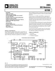
Download HSP45102 12 Bit NCO Data Sheet
Download HSP45102 12 Bit NCO Data Sheet
Download HSP45102 12 Bit NCO Data Sheet

You also want an ePaper? Increase the reach of your titles
YUMPU automatically turns print PDFs into web optimized ePapers that Google loves.
<strong>HSP45102</strong><br />
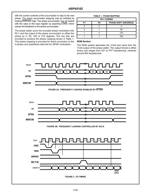
with the current contents of the accumulator to step to the new<br />
phase. The phase accumulator stepping may be inhibited by<br />
holding ENPHAC high. The phase accumulator may be loaded<br />
with the value in the input register by asserting LOAD, which<br />
zeroes the feedback to the phase accumulator.<br />
The phase adder sums the encoded phase modulation bits<br />
P0-1 and the output of the phase accumulator to offset the<br />
phase by 0, 90, 180 or 270 degrees. The two bits are<br />
encoded to produce the phase mapping shown in Table 1.<br />
This phase mapping is provided for direct connection to the<br />
in-phase and quadrature data bits for QPSK modulation.<br />
TABLE 1. PHASE MAPPING<br />
P0-1 CODING<br />
P1 P0 PHASE SHIFT (DEGREES)<br />
0 0 0<br />
0 1 90<br />
1 0 270<br />
1 1 180<br />
ROM Section<br />
The ROM section generates the <strong>12</strong>-bit sine value from the<br />
13-bit output of the phase adder. The output format is offset<br />
binary and ranges from 001 to FFF hexadecimal, centered<br />
around 800 hexadecimal.<br />
SCLK<br />
SD<br />
0 1 2 61 62 63<br />
SFTEN<br />
MSB/LSB<br />
FIGURE 2A. FREQUENCY LOADING ENABLED BY SFTEN<br />
SCLK<br />
SD<br />
0 1 2 61 62 63<br />
SFTEN<br />
MSB/LSB<br />
FIGURE 2B. FREQUENCY LOADING CONTROLLED BY SCLK<br />
CLK<br />
1 2 3 4 5 6 7 8 9 10 11<br />
LOAD<br />
TXFR<br />
ENPHAC<br />
SEL_L/M<br />
OUT0-11<br />
NEW<br />
DATA<br />
FIGURE 3. I/O TIMING<br />
5-50