Accurate Phase Noise Prediction in PLL Synthesizers - Lance Lascari
Accurate Phase Noise Prediction in PLL Synthesizers - Lance Lascari
Accurate Phase Noise Prediction in PLL Synthesizers - Lance Lascari

You also want an ePaper? Increase the reach of your titles
YUMPU automatically turns print PDFs into web optimized ePapers that Google loves.
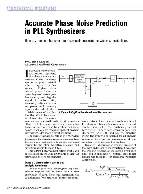
<strong>Accurate</strong> <strong>Phase</strong> <strong>Noise</strong> <strong>Prediction</strong><strong>in</strong> <strong>PLL</strong> <strong>Synthesizers</strong>Here is a method that uses more complete model<strong>in</strong>g for wireless applicationsBy <strong>Lance</strong> <strong>Lascari</strong>Adaptive Broadband CorporationIn modern wireless communicationssystems,the phase noise characteristicsof the frequencysynthesizer play a criticalrole <strong>in</strong> system performance.Higher thandesired phase noise cancause degraded system performanceby reduc<strong>in</strong>g thesignal to noise ratio,<strong>in</strong>creas<strong>in</strong>g adjacent channelpower, and reduc<strong>in</strong>gadjacent channel rejection.While many of the factorsthat affect phase noise<strong>in</strong> phase-locked frequencysynthesizers are well understood, designersoften overlook others. Neglect<strong>in</strong>g these additionalfactors can cause frustration and overdesign,when a more complete up-front analysismay have yielded more elegant solutions.The goal of this article will be to first reviewthe models for standard noise sources and howthese are analyzed, then to do the same for noisecaused by the often forgotten resistors andamplifiers with<strong>in</strong> the loop filter.This is Part 1 of a two-part article. Part 2 willbe published <strong>in</strong> the May 2000 issue of AppliedMicrowave & Wireless magaz<strong>in</strong>e.▲ Figure 1. Z fil3 (f) with optional amplifier <strong>in</strong>serted.Standard phase noise sources andanalysis techniquesThe basic equations describ<strong>in</strong>g the loop’s frequencyresponse will be given with a briefdescription of each. Plots that accompany theequations are from analysis of the test cases presentedlater <strong>in</strong> the article, and are typical for all<strong>PLL</strong> designs. The complete equations <strong>in</strong> contextcan be found <strong>in</strong> [1]. The equations presentedhere and <strong>in</strong> [1] have been drawn <strong>in</strong> part from[4], as well as [3], [6] and [7]. The amplifierwith<strong>in</strong> the loop will be ignored for all analysispresented here, as the implications of thisamplifier will be discussed <strong>in</strong> the text.Equation 1 describes the transfer function ofthe third-order loop filter. Equation 2 describesthe transfer function of the second order loopfilter and is applicable to systems that do notrequire the third pole for additional referencesuppression.Zfil31Zfil( f)×2 × π × f × i × C3( f)=⎛ 1 ⎞Zfil( f)+ R3+ ⎜⎟⎝ 2 × π × f × i×C ⎠3(1)30 · APPLIED MICROWAVE & WIRELESS
R f i CZfil ( f ) ( 1+ 2 × 2× π × × × 2)=[ 2× π × f × i( C + C + R × 2× π × f × i× C × C )]2 1 2 1 2(2)The total forward loop response, G(f), <strong>in</strong>cludes everyth<strong>in</strong>gfrom phase detector to VCO, and is represented byEquation 3. The equation for G_ pd (f) is not <strong>in</strong>cluded, butit represents the transfer function of the discrete-sampl<strong>in</strong>gphase-frequency detector. Details on this functioncan be found <strong>in</strong> [7].▲ Figure 2. Open loop frequency response.Gf ( ) =Kφ× Zfil3( f) × Kvco× amp_ga<strong>in</strong>× G2× π × f × ipd( f)(3)The reverse loop, or feedback ga<strong>in</strong>, is def<strong>in</strong>ed as thereciprocal of the total frequency multiplication factor <strong>in</strong>the loop, N, as shown <strong>in</strong> Equation 4.H= 1NEquation 5 illustrates the open loop ga<strong>in</strong>, G ol (f). Theopen loop ga<strong>in</strong> is the product of equations 3 and 4, show<strong>in</strong>gthe response around the loop. This equation is particularlyuseful for stability analysis. A plot of thisresponse is shown <strong>in</strong> Figure 2.(4)G ol (f):=G(f)×H (5)Because this is a simple negative feedback system, theclosed loop response, G cl (f), at the VCO output is representedby the familiar feedback relationship seen <strong>in</strong>Equation 6. A plot of this response is shown <strong>in</strong> Figure 3.GfGcl ( f ) ( )= 1 + Gf ( ) × H(6)▲ Figure 3. Closed loop frequency response.The well known noise sources (expressed <strong>in</strong> terms ofequivalent noise voltage) are specifically crystal reference(TCXO) noise; phase detector noise; and VCOphase noise.Crystal reference oscillator noise — The crystal oscillatornoise is “amplified” <strong>in</strong> the loop by the ga<strong>in</strong> of theclosed loop transfer function. A simple approximationfor this noise source due to the crystal reference itself, aswith any oscillator, is that it is <strong>in</strong>versely proportional tooffset frequency. Higher order approximations or actualdata could be used if it were available, but the 1/fapproximation is a good start<strong>in</strong>g po<strong>in</strong>t.With<strong>in</strong> the loop bandwidth of the synthesizer, theclosed loop transfer function, G cl (f) is very large <strong>in</strong> magnitude,hence it <strong>in</strong>creases the level of the reference oscillatornoise. This ga<strong>in</strong> is flat until it reaches the loopbandwidth, after which it drops off rapidly. This functionrepresents amplification of the noise with<strong>in</strong> the loopbandwidth, but attenuation of the noise above this frequency.The ga<strong>in</strong> with<strong>in</strong> the loop bandwidth comeslargely from the ratio of the loop division ratio, N, by thereference division ratio, R. If this noise can be observedat all, it is generally seen very close to the carrier (whereit is visible above the other major noise sources).If a TCXO is used, phase noise data should beobta<strong>in</strong>ed from the manufacturer so that reference valuescan be used with the models. Measur<strong>in</strong>g the noise ofa crystal oscillator can be quite difficult s<strong>in</strong>ce the noiseis significantly below the noise of most readily availabletest equipment. In fact, it may be easier to work backwardsfrom measured <strong>PLL</strong> data to determ<strong>in</strong>e the TCXOnoise if the data are not available from the manufacturer.Equation 7 illustrates the noise due to the referenceoscillator, N tcxo (f), at the synthesizer output.Ntcxo⎛ Ntcxo_ref ⎞10⎜⎝ 20⎟⎠ ⎛ 1 ⎞( f) =× ⎜Gcl( f)× ⎟f ⎝ R⎠ftcxo_ref<strong>Phase</strong> detector noise — N p_d (f), is a form of noise thatrepresents the <strong>in</strong>ternal noise floor of the phase/frequencydetector and frequency dividers with<strong>in</strong> the <strong>PLL</strong>. This(7)32 · APPLIED MICROWAVE & WIRELESS
noise is modeled as flat versus frequency and thespecific value for N pd_ref can be obta<strong>in</strong>ed from themanufacturer of the synthesizer IC. For NationalSemiconductor synthesizers (the one used <strong>in</strong> thisarticle, for example), the phase detector noise flooris given for an effective reference frequency of 1Hz. The actual noise floor of the phase detectordegrades proportional to 10*log(F ref /1 Hz). Thisnoise source is flat with respect to frequency, but itis shaped by the closed loop transfer function of thesynthesizer, as shown <strong>in</strong> Equation 8.N ( f) = 10 20 × G ( f)p_d⎛ fref⎞N pd_ref + 10 log⎜⎟⎝ Hz ⎠cl▲ Figure 4. Loop error response.(8)Free-runn<strong>in</strong>g VCO noise — This tends to have thetypical noise profile. The noise is <strong>in</strong>versely proportionalto offset frequency from the carrier. The synthesizedoutput, however, is the result of the <strong>PLL</strong> “clean<strong>in</strong>g up”the close <strong>in</strong> phase noise of the VCO. This compositenoise is calculated <strong>in</strong> Equation 9. The noise of the VCOis effectively high-pass filtered by the <strong>PLL</strong>, provid<strong>in</strong>grejection of phase noise or phase error with<strong>in</strong> the bandwidth,but leav<strong>in</strong>g VCO noise well outside of the loopbandwidth unaffected. A plot of this high-pass filterfunction provided by the <strong>PLL</strong> is shown <strong>in</strong> Figure 4.Nvco( f)=A plot of the commonly analyzed phase noise sourcesdescribed above at the synthesizer output is shown <strong>in</strong>Figure 5.Models for noise <strong>in</strong> a typical third order loop filterPrior to delv<strong>in</strong>g <strong>in</strong>to the circuit equations, it is importantto outl<strong>in</strong>e the methodology that will be employed toanalyze the problem. The approach used will be to firstdeterm<strong>in</strong>e the voltage at the <strong>in</strong>put of the VCO due toeach of the noise sources <strong>in</strong> the loop. This voltage willthen be used to calculate the equivalent FrequencyModulation (FM) (i.e. phase noise) at the VCO outputdue to each of these sources us<strong>in</strong>g the VCO ga<strong>in</strong>, K vco .A key parameter used to analyze frequency modulationis the modulation <strong>in</strong>dex, m, calculated us<strong>in</strong>gEquation 10.m =df m⎛ Nvco_ref ⎞10⎜⎝ 20⎟⎠ ⎛ 1×f ⎜⎝ 1 + Gfvco_ref⎞⎟( f)⎠(9)(10)where m = modulation <strong>in</strong>dex=peak phase deviation <strong>in</strong>radians; d = frequency deviation; and f m =message orol▲ Figure 5. TCXO, phase detector and VCO noise.modulat<strong>in</strong>g frequency.In the case of a “direct” FM system, where the modulation/messageis fed directly to the VCO <strong>in</strong> the form ofvoltage, the frequency deviation is simply the product ofthe modulation voltage and the tun<strong>in</strong>g sensitivity (volts× Hz/volt = Hz).If the peak phase deviation is well below one radian,as is the case with all that will be studied here, the higherorder Bessel functions can be ignored and the relativelevel of the sidebands on the carrier due to the modulat<strong>in</strong>gfrequency can be calculated us<strong>in</strong>g Equation 11, seereference [5] for further detail on this subject.sideband_level⎛ m⎞= 20log⎜⎟⎝ 2 ⎠(11)These simple equations for frequency/phase modulationform the basis for the analysis of phase noise due tovoltage noise sources with<strong>in</strong> the loop hardware.Calculat<strong>in</strong>g the noise voltages <strong>in</strong> the loopS<strong>in</strong>ce the noise sources appear <strong>in</strong> different circuitnodes throughout the loop, the frequency response ofthe transfer function between each source and the VCO<strong>in</strong>put will be different. This, <strong>in</strong> turn, results <strong>in</strong> modulationat the VCO output unique to each source <strong>in</strong> frequencyand magnitude.It is important to realize that <strong>in</strong> a system such as this,the resistor or op-amp noise modulates the VCO even ifa <strong>PLL</strong> were not connected — so the “corruption” due to34 · APPLIED MICROWAVE & WIRELESS
the resistors and op-amp can be consideredan open-loop phenomenon.However the net result <strong>in</strong> the synthesizedoutput requires the closed loopresponse, and the analysis is identicalto the analysis used to show the effectof the <strong>PLL</strong> on the stand-alone VCOphase noise <strong>in</strong> Equation 9. Valuable<strong>in</strong>sight can be ga<strong>in</strong>ed by observ<strong>in</strong>g theopen and closed loop SSB phase noisecurves rather than just look<strong>in</strong>g at thetotal output phase noise of the closedloop system. The connection betweenthe open and closed loop responses, isthe high-pass transfer function plotted<strong>in</strong> Figure 4, sometimes referred to asthe error response of the loop.The validity of the open-loop analysistechnique requires the assumptionthat the charge pump does not loaddown the loop filter excessively. Thefollow<strong>in</strong>g key po<strong>in</strong>ts support thisassumption. First, when <strong>in</strong> lock, thecharge pump does very little but providevery m<strong>in</strong>or corrections to keep theloop locked. Second, the charge pumpis made up of a current source and acurrent s<strong>in</strong>k, both of which represent ahigh impedance when operat<strong>in</strong>g <strong>in</strong> al<strong>in</strong>ear region. The closed-loop action ofthe synthesizer fights the resistor andop-amp noise, but that is adequatelydescribed by the analysis of the closedloop system.<strong>Noise</strong> found <strong>in</strong> resistorsRandom electron motion <strong>in</strong>side of ord<strong>in</strong>ary resistorsmakes for a “built-<strong>in</strong>” noise source <strong>in</strong> every circuit conta<strong>in</strong><strong>in</strong>gresistors. The noise is white <strong>in</strong> nature [8], withit’s power <strong>in</strong> watts dissipated <strong>in</strong> an equivalent 1 ohmresistor is shown <strong>in</strong> Equation 12, and the units arevolts 2 /Hz.P ( R)= 4 × k× Temp × B×Rresistor_noise(12)Thus, Equation 13 computes the equivalent RMSnoise voltage generated <strong>in</strong> a known resistanceV ( R)= 4 × k× Temp × R×Bresistor_noise(13)where k = Boltzmann’s constant; Temp = temperature<strong>in</strong> kelv<strong>in</strong>s; B = bandwidth <strong>in</strong> Hz; and R = resistance <strong>in</strong>ohms. For most of our analysis we will use a bandwidthof 1 Hz.These equations simply show the equivalent noisevoltage source that appears <strong>in</strong> series with each resistor.▲ Figure 6. (a) R2 noise model with or without op-amp; (b) R3 noise modelwithout op-amp; (c) R3 noise model with op-amp, assum<strong>in</strong>g that the op-amphas very low output impedance.Note that the noise could just as easily be modeled as anoise current source <strong>in</strong> parallel with the resistor.References [2] and [8] provide details on the noise <strong>in</strong>resistors and op-amps. When crunch<strong>in</strong>g the numbers fortypical resistor values, one may <strong>in</strong>itially dismiss the voltagesas m<strong>in</strong>uscule. As we will show later, even nanovoltsof noise can cause several dB of degradation <strong>in</strong> the s<strong>in</strong>gle-sidebandphase noise of a synthesizer because K vco isoften a very large number.Figure 6 shows the basic <strong>PLL</strong> loop filter and wherethe noise sources appear. The charge pump connectionto the <strong>PLL</strong> has been left out for these models because itrepresents a very high impedance when the loop islocked. As previously stated, the <strong>in</strong>itial analysis of theresistor noise will be done “open loop,” and the effects ofthe <strong>PLL</strong> on shap<strong>in</strong>g this noise further will be <strong>in</strong>vestigatedafter the basic models are developed.S<strong>in</strong>ce the noise sources are uncorrelated, each resistoris analyzed separately and the effects are added at alater stage. Deriv<strong>in</strong>g the actual noise voltage versus frequencyat the <strong>in</strong>put to the VCO tun<strong>in</strong>g port is a matterof basic circuit analysis us<strong>in</strong>g the models <strong>in</strong> Figure 6.36 · APPLIED MICROWAVE & WIRELESS
Resistor noise analysis for the“case 2” example <strong>PLL</strong> <strong>in</strong> this articlethat will be discussed later is shown<strong>in</strong> Figure 7 and Figure 8. Figure 7shows the baseband noise voltages atthe VCO <strong>in</strong>put <strong>in</strong> the open loop case,and Figure 8 shows the noise contributionto the synthesizer output. ■References1. Complete MathCAD Analysisused <strong>in</strong> this article is available <strong>in</strong>MathCAD and PDF formats athttp://home.rochester.rr.com/lascari/lancepll.zip.2. W.P. Rob<strong>in</strong>s, <strong>Phase</strong> <strong>Noise</strong> <strong>in</strong>Signal Sources: Theory andApplications, W.P. Rob<strong>in</strong>s, 1984.3. James A. Crawford, FrequencySynthesizer Design Handbook,Artech House, 1994.4. Dean Banerjee, <strong>PLL</strong>Performance, Simulation, andDesign, http://www.national.com/app<strong>in</strong>fo/wireless/deansbook.pdf.5. A. Bruce Carlson, CommunicationSystems: An Introduction toSignals and <strong>Noise</strong> <strong>in</strong> ElectricalCommunication, McGraw-Hill, 1986.6. William O. Keese, “An Analysisand Performance Evaluation ofPassive Filter Design Technique forCharge Pump <strong>Phase</strong>-Locked Loops,”Application Note 1001, NationalSemiconductor.7. Jeff Blake, “Design of WidebandFrequency <strong>Synthesizers</strong>,” RF Design,May 1988.8. “<strong>Noise</strong> Specs Confus<strong>in</strong>g,”Application Note 104, NationalSemiconductor.Figure Analysis Conditions Comments6a R2 Without op-amp Assume the op-amp is not presentand the R2 noise must be calculatedthrought the entire network.6a R2 With op-amp Assume for R2 noise analysis the opamp<strong>in</strong>put impedance is <strong>in</strong>f<strong>in</strong>ite, andthe R2 noise out of the network consist<strong>in</strong>gof R2, C1 and C2 is determ<strong>in</strong>ed.This noise is then amplified byamp_ga<strong>in</strong> before be<strong>in</strong>g passedthrough the network consist<strong>in</strong>g of R3and C3.6b R3 Without op-amp In this case, the R3 noise source is“float<strong>in</strong>g” <strong>in</strong> the loop filter network,and the transfer function between thissource and the output of the network<strong>in</strong>cludes the impedances of all the filtercomponents.6c R3 With op-amp S<strong>in</strong>ce the op-amp output impedancewill be assumed to be very low, wemodel this as a short. Hence, this isthe simplest model of all, R3 shortedto ground.▲ Table 1. Description of the resistor noise models shown <strong>in</strong> Figure 6.<strong>Noise</strong> <strong>in</strong> microvolts▲ Figure 7. Baseband noise voltages at the VCO <strong>in</strong>put <strong>in</strong> the open-loop state.▲ Figure 8. Resistor noise contributions at the VCO output after the <strong>PLL</strong>’s highpasserror function is <strong>in</strong>cluded.Author <strong>in</strong>formation<strong>Lance</strong> <strong>Lascari</strong> is a Pr<strong>in</strong>cipalEng<strong>in</strong>eer at Adaptive BroadbandCorporation <strong>in</strong> Rochester, NY. He hasbeen work<strong>in</strong>g as an RF designer onthe company’s QAM Po<strong>in</strong>t-Po<strong>in</strong>t andFSK Po<strong>in</strong>t-Multipo<strong>in</strong>t products forthe past five years. He earned aBSEE from the RensselaerPolytechnic Institute <strong>in</strong> 1995. Hisprofessional <strong>in</strong>terests <strong>in</strong>clude lownoisesynthesizer and VCO design,design for high l<strong>in</strong>earity, and low-cost transceiverdesign. He may be reached via email at llascari@adaptivebroadband.com,or through his web page:http://home.rochester.rr.com/lascari.38 · APPLIED MICROWAVE & WIRELESS