Processing Gain for Direct Sequence Spread Spectrum ...
Processing Gain for Direct Sequence Spread Spectrum ...
Processing Gain for Direct Sequence Spread Spectrum ...
You also want an ePaper? Increase the reach of your titles
YUMPU automatically turns print PDFs into web optimized ePapers that Google loves.
Harris Semiconductor<br />
No. AN9633 August 1996 Harris Wireless Products<br />
<strong>Processing</strong> <strong>Gain</strong> <strong>for</strong> <strong>Direct</strong> <strong>Sequence</strong><br />
<strong>Spread</strong> <strong>Spectrum</strong> Communication Systems and PRISM<br />
Authors: John Fakatselis, Harris Corporation Semiconductor Sector<br />
Madjid A. Belkerdid<br />
Electrical and Computer Engineering Department<br />
University of Central Florida<br />
Orlando, FL 32816<br />
TM<br />
Introduction<br />
DSSS Transceiver<br />
This application note addresses<br />
the concept of processing gain<br />
(PG) of <strong>Direct</strong> <strong>Sequence</strong><br />
<strong>Spread</strong> <strong>Spectrum</strong> (DSSS)<br />
systems. The PRISM chipset is used to implement DSSS<br />
radio designs. The processing gain provides the unique<br />
properties to the DSSS wave<strong>for</strong>m primarily in terms of interference<br />
tolerance. The PG of a DSSS system is centered<br />
around the utilization of random codes which are used in<br />
conjunction with the data. These random codes are referred<br />
as Pseudo Noise (PN) codes. The HSP3824 provides this<br />
coding capability <strong>for</strong> the PRISM.<br />
Description<br />
In a DSSS system random binary data with a bit rate of r b<br />
bits per sec (bps) is multiplied (Exclusive Ored) by a<br />
pseudorandom binary wave<strong>for</strong>m, which is at much higher<br />
rate and it provides the frequency spreading operation. This<br />
pseudorandom (PN) binary source outputs symbols called<br />
chips at a constant chip rate r C chips per sec (cps).This is a<br />
random, noise like signal and hence the name PN signal.<br />
The chip rate is always higher than the bit rate, and the ratio<br />
of the chip rate to the bit rate is defined as the processing<br />
gain (PG) [2]. The PG is a true signal to jammer (interference)<br />
ratio at the receiver after the despreading operation<br />
(removal of PN).<br />
The rate of the PN code is the one that defines the<br />
bandwidth of the transmitted spread wave<strong>for</strong>m.<br />
The receiver of a DSSS system must remove the spreading<br />
as the first step in the demodulation process.<br />
During the despreading operation the receiver must<br />
generate a phase locked exact replica of the pseudorandom<br />
spreading wave<strong>for</strong>m to match the transmitted signal. This is<br />
achieved by the code acquisition, and code tracking loops<br />
embedded in the HSP3824. The receiver PN sequence must<br />
be exactly in phase with the transmitted PN sequence, and<br />
this is achieved by correlation techniques.<br />
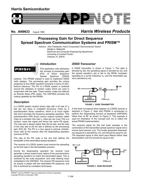
A DSSS transmitter is shown in Figure 1. The data is<br />
denoted by d(t), the spreading signal is denoted by c(t), and<br />
the spread wave<strong>for</strong>m q(t) is fed to the BPSK modulator<br />
operating at a carrier frequency f C , and the transmitted signal<br />
is denoted by x(t).<br />
d(t)<br />
c(t)<br />
CODE<br />
GENERATOR<br />
q(t)<br />
COS(ω O t)<br />
FIGURE 1. DSSS TRANSMITTER<br />
A text book conceptual block diagram of a DSSS receiver is<br />
depicted in Figure 2. Note that PRISM is architected to<br />
per<strong>for</strong>m the despreading function at baseband (HSP3824)<br />
rather than at RF as shown on Figure 2. This example is<br />
used <strong>for</strong> illustration of the concept and not to reflect the<br />
actual PRISM implementation.<br />
The received signal <strong>for</strong> this text book example is the<br />
combination of the transmitted spread spectrum signal and a<br />
narrow band jammer x J (t). The locally generated despreading<br />
sequence is denoted by c’(t), and should be equal to c(t).<br />
The despread signal is then band pass filtered be<strong>for</strong>e data<br />
demodulation and d’(t) should be equal to d(t).<br />
x(t) + x j (t)<br />
c’(t)<br />
PN<br />
GENERATOR<br />
x’(t)<br />
BPF<br />
H(f)<br />
y(t)<br />
COS(ω O t)<br />
FIGURE 2. DSSS RECEIVER<br />
LPF<br />
x(t)<br />
d’(t)<br />
PRISM and the PRISM logo are trademarks of Harris Corporation.<br />
Copyright © Harris Corporation 1996<br />
7-106
Application Note 9633<br />
PG Benefits<br />
The primary benefit of processing gain is its contribution<br />
towards jamming resistance to the DSSS signal. The PN<br />
code spreads the transmitted signal in bandwidth and it<br />
makes it less susceptible to narrowband interference within<br />
the spread BW. The receiver of a DSSS system can be<br />
viewed as unspreading the intended signal and at the same<br />
time spreading the interfering wave<strong>for</strong>m. This operation is<br />
best illustrated on Figure 3.<br />
Figure 3 depicts the power spectral density (psd) functions<br />
of the signals at the receiver input, the despread signal, the<br />
bandpass filter power transfer function, and the band pass<br />
filter output. Figure 3 graphically describes the effect of the<br />
processing gain on a jammer. The jammer is narrow, and<br />
has a highly peaked psd, while the psd of the DSSS is wide<br />
and low. The despreading operation spreads the jammer<br />
power psd and lowers its peak, and the BPF output shows<br />
the effect on the signal to jammer ratio.<br />
If <strong>for</strong> example, BPSK modulation is used and an Eb/No of<br />
lets say 14dB is required to achieve a certain BER<br />
per<strong>for</strong>mance, when this wave<strong>for</strong>m is spread with a processing<br />
gain of 10dB then the receiver can still achieve its<br />
required per<strong>for</strong>mance with the signal having a 4dB power<br />
advantage over the interference. This is derived from the<br />
14dB required minus the 10dB of PG.<br />
The higher the processing gain of the DSSS wave<strong>for</strong>m the<br />
more the resistance to interference of the DSSS signal.<br />
The classical definition of processing gain is the 10 Log<br />
number [r C /r B ] in dB. By this definition a system that has a<br />
data rate of 1MBPS and a chip rate (rate of PN code) of<br />
1MCPS will have a PG of 10.41dB. Using the PRISM chip<br />
set each data bit is x-ored with an 11 bit sequence <strong>for</strong> this<br />
particular example. The processing gain can be then viewed<br />
as the 10Log[11]dB where 11 is the length of the PN code. If<br />
a code with a length of 16 bits is to be used then the processing<br />
gain is equivalent to 10 Log[16] dB or 12.04dB.<br />
To this end these PN signals must posses certain mathematical<br />
properties to be useful as part of a DSSS system.<br />
Primarily the PN codes that are useful must have very good<br />
autocorrelation and crosscorrelation properties as well as<br />
maintaining some randomness properties.<br />
The DSSS receiver is utilizing a reference PN sequence<br />
which is a replica to the transmitted sequence and when it<br />
detects correlation between the reference and the incoming<br />
sequences it declares initial acquisition and it establishes<br />
initial symbol timing. Any partial correlations can result to<br />
false acquisitions and degradation to the receiver<br />
per<strong>for</strong>mance. This is why the PN code must have good<br />
correlation properties. Some of the PN code classes with<br />
such properties are described next.<br />
This paper highlights the Barker codes, Willard codes and<br />
m-sequences with 7 and 15 chips per period which are<br />
implementable using the HSP3824.<br />
S X (f) + S J (f)<br />
JAMMER PSD<br />
SPREAD SPECTRUM<br />
SIGNAL PSD<br />
T B /2<br />
S X (f)<br />
DESPREAD<br />
SIGNAL<br />
DESPREAD<br />
JAMMER<br />
T c /2<br />
JT C /2<br />
f C<br />
f<br />
f C<br />
FIGURE 3A. PSD OF SPREAD SPECTRUM SIGNAL AND NAR-<br />
ROWBAND JAMMER<br />
FIGURE 3B. PSD OF DESPREAD SIGNAL AND JAMMER<br />
S Y (f)<br />
|H(f)| 2 f C<br />
f<br />
T B /2<br />
SIGNAL<br />
1<br />
JAMMER<br />
JT C /2<br />
f<br />
f C<br />
FIGURE 3C. POWER TRANSFER FUNCTION OF BPF<br />
FIGURE 3D. PSD OF BPF OUTPUT<br />
FIGURE 3. PROCESSING GAIN EFFECT ON NARROW BAND JAMMING<br />
7-107
PN Codes<br />
PN codes with the mathematical properties required <strong>for</strong><br />
implementation of a DSSS radio are:<br />
Maximum Length <strong>Sequence</strong>s<br />
Maximum length sequences (m-sequences), are PN<br />
sequences that repeat every 2 n -1, where n is an integer,<br />
they are implemented by shift registers and Exclusive Or<br />
gates, they are governed by primitive polynomials, and possess<br />
good randomness properties including a two-valued<br />
autocorrelation function [3].<br />
For example the 7 chip PN sequence is governed by the<br />
primitive polynomial generator<br />
c 7 (x) = 1 + x 2 + x 3<br />
and the output chips are given by:<br />
0 0 1 0 1 1 1 0 0 1 0 1 1 1 0 0 1 0 1 1 1 0 0 1 0 1 1 10...<br />
Application Note 9633<br />
Barker Codes<br />
Barker Codes are short unique codes that exhibit very good<br />
correlation properties. These short codes with N bits, with<br />
N=3 to 13, are very well suited <strong>for</strong> DSSS applications and<br />
can all be generated by the HSP3824. A list of Barker Codes<br />
is tabulated in Table 1.<br />
Willard Codes<br />
Willard Codes, found by computer simulation and optimization,<br />
and under certain conditions, offer better per<strong>for</strong>mance<br />
than Barker Codes. They can all be generated by the<br />
HSP3824, as was done <strong>for</strong> the Barker Codes. A list of<br />
Willard Codes is provided in Table 1.<br />
The inverted or bit reversed versions of the codes listed on<br />
Table 1 can be used since they still maintain the desired<br />
autocorrelation properties.<br />
-7T C -1/7<br />
with different spreading parameters <strong>for</strong> each direction.<br />
TABLE 1. BARKER AND WILLARD CODES<br />
BARKER<br />
WILLARD<br />
Figure 4 depicts the d(t), c(t) with the above m-sequence, N<br />
SEQUENCES<br />
SEQUENCES<br />
and with q(t) the x-or of d(t) and (ct).<br />
3 110 110<br />
1<br />
0<br />
4 1110 or 1101 1100<br />
5 11101 11010<br />
7 1110010 1110100<br />
d(t)<br />
T B<br />
t<br />
11 11100010010 11101101000<br />
13 1111100110101 1111100101000<br />
c(t)<br />
t<br />
T C<br />
7T C<br />
Configuring the HSP3824 to<br />
Implement Various PN Codes<br />
q(t)<br />
t The HSP3824 is the baseband processor of the PRISM<br />
chipset and it generates the PN sequence. The device is<br />
FIGURE 4. TIME DOMAIN SIGNALS WITH PG = 7 programmable to any desirable sequence of up to 16 bits.<br />
Figure 5 depicts the 7 chip sequence and its autocorrelation PN Generator Description<br />
function. Note that the autocorrelation also repeats every 7 The spread function <strong>for</strong> the radio is the same sequence and<br />
chips, or once per bit of the actual data if each of the data is applied to every symbol as BPSK modulation. PN generation<br />
is per<strong>for</strong>med by parallel loading the sequence from a<br />
bits is spread by the entire sequence.<br />
As another example, the 15 chip PN sequence is governed configuration register (CR) within the HSP3824 and serially<br />
by the primitive polynomial generator<br />
shifting it out to the modulator.<br />
c 15 (x) = 1 + x 3 + x 4<br />
PN Generator Programmable Registers<br />
A maximum of 16 bits can be programmed into the configuration<br />
register. Registers CR13 and CR14 contain the high<br />
and the output chips are given by:<br />
0 0 0 1 0 0 1 1 0 1 0 1 1 1 1 0 0 0 1 0 0 1 1 0 1 0 1 1 1 1 and low bytes of the sequence <strong>for</strong> the transmitter. The<br />
0 0 0 1 0 0 1 1 0 1 0 1 1 1 1...<br />
corresponding registers <strong>for</strong> the receiver are CR20 & CR21.<br />
Bits 5 & 6 of CR3 set the sequence length in chips per bit.<br />
c(t)<br />
The sequence is transmitted MSB first. When fewer than 16<br />
bits are in the sequence, the MSBs are truncated.<br />
1<br />
t<br />
0 T C<br />
PN Correlator Description<br />
-1<br />
The PN correlator is designed to handle BPSK spreading.<br />
R(t)<br />
Since the spreading is BPSK, the correlator is implemented<br />
1<br />
with two real correlators, one <strong>for</strong> the I and one <strong>for</strong> the Q<br />
channel. It has programmable registers to hold the<br />
spreading sequence and the sequence length <strong>for</strong> both the<br />
T C<br />
t receiver and the transmitter. This allows a full duplex link<br />
7T C<br />
FIGURE 5. SEVEN CHIP M-SEQUENCE AND ITS AUTOCOR-<br />
RELATION FUNCTION<br />
The correlators are time invariant matched filters otherwise<br />
known as parallel correlators.<br />
7-108
Application Note 9658<br />
References<br />
[1] R. L. Pickholtz, D. L. Schilling, and L. B. Milstein,<br />
“Theory of <strong>Spread</strong>-<strong>Spectrum</strong> Communications - A<br />
Tutorial”, IEEE Trans. Comm., vol COM-30, May 1982.<br />
[2] R. C. Dixon, “<strong>Spread</strong> <strong>Spectrum</strong> Systems”. New York:<br />
Wiley-Interscience, 1984.<br />
[3] R. L. Peterson, R. E. Ziemer, and D. E. Borth, “Introduction<br />
to <strong>Spread</strong> <strong>Spectrum</strong> Communications”. Inglewood<br />
Cliffs, NJ: Prentice Hall, 1995.<br />
All Harris Semiconductor products are manufactured, assembled and tested under ISO9000 quality systems certification.<br />
Harris Semiconductor products are sold by description only. Harris Semiconductor reserves the right to make changes in circuit design and/or specifications at<br />
any time without notice. Accordingly, the reader is cautioned to verify that data sheets are current be<strong>for</strong>e placing orders. In<strong>for</strong>mation furnished by Harris is<br />
believed to be accurate and reliable. However, no responsibility is assumed by Harris or its subsidiaries <strong>for</strong> its use; nor <strong>for</strong> any infringements of patents or other<br />
rights of third parties which may result from its use. No license is granted by implication or otherwise under any patent or patent rights of Harris or its subsidiaries.<br />
Sales Office Headquarters<br />
NORTH AMERICA<br />
Harris Semiconductor<br />
P. O. Box 883, Mail Stop 53-210<br />
Melbourne, FL 32902<br />
TEL: 1-800-442-7747<br />
(407) 729-4984<br />
FAX: (407) 729-5321<br />
For general in<strong>for</strong>mation regarding Harris Semiconductor and its products, call 1-800-4-HARRIS<br />
EUROPE<br />
Harris Semiconductor<br />
Mercure Center<br />
100, Rue de la Fusee<br />
1130 Brussels, Belgium<br />
TEL: (32) 2.724.2111<br />
FAX: (32) 2.724.22.05<br />
ASIA<br />
Harris Semiconductor PTE Ltd.<br />
No. 1 Tannery Road<br />
Cencon 1, #09-01<br />
Singapore 1334<br />
TEL: (65) 748-4200<br />
FAX: (65) 748-0400<br />
SEMICONDUCTOR<br />
7-109


