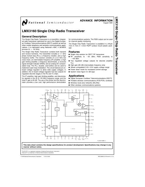
LMX3160 Single Chip Radio Transceiver
LMX3160 Single Chip Radio Transceiver
LMX3160 Single Chip Radio Transceiver
- No tags were found...

Create successful ePaper yourself
Turn your PDF publications into a flip-book with our unique Google optimized e-Paper software.
<strong>LMX3160</strong> <strong>Single</strong> <strong>Chip</strong> <strong>Radio</strong> <strong>Transceiver</strong>General DescriptionThe <strong>Single</strong> <strong>Chip</strong> <strong>Radio</strong> <strong>Transceiver</strong> is a monolithic integratedradio transceiver optimized for use in the Digital EuropeanCordless Telecommunications (DECT) system as well asother mobile telephony and wireless communications applicationsIt is fabricated using National’s ABiC V BiCMOSprocess (f T e 18 GHz)The <strong>Single</strong> <strong>Chip</strong> <strong>Radio</strong> <strong>Transceiver</strong> contains both transmitand receive functions The transmitter includes a 11 GHzphase locked loop (PLL) a frequency doubler and a highfrequency buffer The receiver consists of a 20 GHz lownoise mixer an intermediate frequency (IF) amplifier a highgain limiting amplifier a frequency discriminator a receivedsignal strength indicator (RSSI) and an analog DC compensationloop The PLL doubler and buffers can be used toimplement open loop modulation The circuit features an onboardvoltage regulator to allow wide supply voltages Inaddition the on board voltage regulator has two outputs forregulated discrete stages in the Rx and Tx chainThe IF amplifier high gain limiting amplifier and discriminatoroperate in the 40 to 150 MHz frequency range and thetotal IF gain is 85 dB The use of the limiter and the discriminatorprovides a low cost high performance demodulatorADVANCE INFORMATIONAugust 1995for communications systems The RSSI output can be usedfor channel quality monitoringThe <strong>Single</strong> <strong>Chip</strong> <strong>Radio</strong> <strong>Transceiver</strong> is available in a 48-pin7mm X 7mm X 14mm PQFP surface mount plastic packageFeaturesY <strong>Single</strong> chip solution for DECT RF transceiverY RF sensitivity to b93 dBm RSSI sensitivity tob100 dBmY Two regulated voltage outputs for discrete amplifierV CCY High gain (85 dB) intermediate frequency stripY Allows unregulated 30V–55V supply voltage rangeY Power down mode for increased current savingsY System noise figure 54 dB (typ)ApplicationsYYYYDigital European Cordless Telecommunications (DECT)Portable wireless communications (PCSPCN cordless)Wireless local area networks (WLANs)Other wireless communications systems<strong>LMX3160</strong> <strong>Single</strong> <strong>Chip</strong> <strong>Radio</strong> <strong>Transceiver</strong>TLW12493–1This data sheet contains the design specifications for product development Specifications may change in anymanner without noticeTRI-STATE is a registered trademark of National Semiconductor CorporationFastLockTM is a trademark of National Semiconductor CorporationC1995 National Semiconductor CorporationTLW12493RRD-B30M115Printed in U S A
<strong>LMX3160</strong> Pin DiagramTLW12493–2Pin No Pin Name IO Description1 V CC Power supply voltage input to mixer Connect to VBAT2 MIXER OUT O IF output signal of the mixer3 V CC Power supply voltage input to mixer Connect to VBAT4 GND Ground5 RF IN I RF input to the mixer6 GND Ground7 TxV REG O Supply voltage to external gain stage8 V CC Power supply voltage input to analog sections of doublerPLL Connect to VBAT9 GND Ground10 Tx OUT O Doubler output11 GND Ground12 V CC Power supply voltage input to analog sections of doublerPLL Connect to VBAT13 GND Ground14 GND Ground15 f IN I RF Input to doubler and PLL16 CE I <strong>Chip</strong> Enable LOW powers down entire part Before taking HIGH all mwire instructions should beloaded for R N F latches Taking CE HIGH will power up the appropriate chip blocks depending onthe state of bits F6 F7 F14 and F15 The CE state change will also load the PLL N and R countersto the correct divide ratios2
<strong>LMX3160</strong> Pin Diagram (Continued)Pin No Pin Name IO Description17 V P Power supply for charge pump18 D o O Internal charge pump output For connection to a loop filter for driving the input of an externalVCO19 V CC Power supply input for CMOS section of PLL Connect to VBAT20 GND Ground21 Out 0FL o IO Programmable CMOS output Can be used for FastLockTM output (See Programmable Modes)22 Out 1Rx PD IO Programmable CMOS output Can be used for hardwire receiver power down (See ProgrammableModes)23 Out 2Tx PD IO Programmable CMOS output Can be used for hardwire transmitter power down (SeeProgrammable Modes)24 PLL PD I PLL PD e LOW for PLL normal operations PLL PD e HIGH for PLL power saving25 Clock I High impedance CMOS clock input26 Data I Binary serial data input Data entered MSB first High impedance CMOS input27 LE I Load enable input28 OSC IN I Oscillator input29 S Field I DC compensation circuit enable While LOW the DC compensation circuit is enabled and thethreshold is updated through the DC compensation loop While HIGH the switch is opened andthe comparator is held by the external capacitor30 RSSI OUT O Voltage output of the received signal strength indicator (RSSI)31 Thresh O Threshold level to external comparator32 DC COMP IN I Input to DC compensation circuit33 DISC OUT O Demodulated output of discriminator34 GND Ground35 V CC Power supply input to discriminator circuit Connect to VBAT36 QUAD IN I Quadrature input37 V CC Power supply input to limiter output stage Connect to VBAT38 GND Ground39 LIM OUT O Limiter output to the quadrature tank40 GND Ground41 V CC Power supply input for limiter Connect to VBAT42 LIM IN I IF input to the limiter43 GND Ground44 GND Ground45 IF OUT O IF output to bandpass filter46 V CC Power supply input for IF amplifier Connect to VBAT47 IF IN I IF input to IF amplifier48 Rx V REG Supply voltage to external LNA3
Absolute Maximum Ratings (Note 1)If MilitaryAerospace specified devices are requiredplease contact the National Semiconductor SalesOfficeDistributors for availability and specificationsPower Supply Voltage (V CC )b03V to a65VV Pb03V to a65VVoltage on Any Pin withGND e 0V (V I )b03V to a65VStorage Temperature Range (T S ) b65Ctoa150CLead Temp (solder 4 sec)(T L )a260CNote 1 Absolute Maximum Ratings indicate limits beyond which damage tothe device may occur Operating Ratings indicate conditions for which thedevice is intended to be functional but do not guarantee specific performancelimits For guaranteed specifications and test conditions see the ElectricalCharacteristics The guaranteed specifications apply only for the testconditions listedRecommended OperatingConditionsSupply Voltage (V CC )Operating Temperature (T A )30V to 55Vb10Ctoa70CElectrical CharacteristicsThe following specifications are guaranteed over the recommended operating conditions unless otherwise specifiedSymbol Parameter Conditions Min Typ Max UnitsRx I CC Receive Mode Current Consumption Tx PLL Powered Down38 45 mA(Note 1)Tx I CC Transmit Mode Current Consumption Rx PLL Powered Down(Note 2)20 25 mAI PD Power Down Current Tx Rx PLL Off 1 10 mAf RF RF Frequency Range 17 20 GHzf max Maximum IF Input Frequency 120 150 MHzf min Minimum IF Input Frequency 18 20 MHzMIXERf IN e 19 GHzNF <strong>Single</strong> Side Band Noise Figure 59 7 dBGA Gain 16 18 dBOIP3 Output Intercept Point b2 1 dBmRF–RL RF Return Loss Z o e 50X 15 dBIF–RL IF Return Loss Z o e 200X 15 dBf IN –RF f IN to RF Isolation 30 dBf IN –IF f IN to IF Isolation 30 dBRF–IF RF to IF Isolation 30 dB4
Electrical Characteristics The following specifications are guaranteed over the recommended operating conditionsunless otherwise specified (Continued)Symbol Parameter Conditions Min Typ Max UnitIF AMPLIFIERf IN e 120 MHzNF Noise Figure 6 8 dBAv Gain 20 25 dBOIP3 Output Intercept Point 6 7 dBmZ IN Input Impedance 200 XZ OUT Output Impedance 200 XIF LIMITERf IN e 120 MHzNF IF Limiter Noise Figure 10 12 dBAv Limiter Gain 55 60 dBSens LimiterDisc Sensitivity BER e 10b3 b65 dBmIF IN IF Limiter Input Impedance 200 XIF OUT IF Limiter Output Impedance 1000 XV max Maximum Input Voltage Level 500 mV PPV OUT Output Swing 500 mV PPDISCRIMINATORDynamic Range 60 dBf IN e 120 MHzV OUT Discriminator Output Peak to Peak Voltage 250 400 mVV OS Disc Output DC Voltage 14 17 VDISC OUT Disc Output Impedance 150 XRSSIf IN e 120 MHzRSSI RSSI Dynamic Range 70 80 dBRSSI OUT RSSI Output Voltage Pin eb85 dBm 01 025 04 VFREQUENCY DOUBLERPin e 0 dBm 115 15 18 VRSSI Slope Pin eb75 to b25 dBm 11 20 mVdBRSSI Linearity 3 dBf OUT e 189 GHzf IN Input Frequency Range 885 950 MHzV IN Input Signal Level Z IN e 200X b14 b115 b9 dBmZ o Output Impedance 45 60 80 XFundamental Rejection (Note 3) V IN e 450 mV PP 30 dBHarmonic Suppression (Note 3) V IN e 450 mV PP 20 dBP OUT Output Power b10 b8 dBm5
Electrical Characteristics The following specifications are guaranteed over the recommended operating conditionsunless otherwise specified (Continued)Symbol Parameter Conditions Min Typ Max UnitFREQUENCY SYNTHESIZERV OSC Oscillator Sensitivity 05 10 V PPI Do-source Charge Pump Output Current V do e V P 2 I cpo e LOW (Note 4) b15 mAI Do-sink V do e V P 2 I cpo e LOW (Note 4) 15 mAI Do-source V do e V P 2 I cpo e HIGH (Note 4) b60 mAI Do-sink V do e V P 2 I cpo e HIGH (Note 4) 60 mAI Do-Tri05 s V dos V P b05T A e 25Cb10 01 10 nAV OH High-Level Output Voltage I OH eb10 mA V CC b04 VV OL Low-Level Output Voltage I OL e 10 mA 04 VV IH High-Level Input Voltage V CC b08 VV IL Low-Level Input Voltage 08 VI IN Input Current GND k V INk V CC b10 10 mAt CS Data to Clock Set Up Time See Data Input Timing 50 nst CH Data to Clock Hold Time See Data Input Timing 10 nst CWH Clock Pulse Width High See Data Input Timing 50 nst CWL Clock Pulse Width Low See Data Input Timing 50 nst ES Clock to Load Enable Set Up Time See Data Input Timing 50 nst EW Load Enable Pulse Width See Data Input Timing 50 nsDC COMPENSATION SAMPLE AND HOLD CIRCUITV OS Input Offset Voltage 3 mVV IO InputOutput Voltage Swing Centered at 15V 10 V PPR SH Sample and Hold Resistor 224 336 XD V Threshold Input Voltage Droop C hold e 2700 pF 1 10 mVmsNote 1 This includes 5 mA current sourced from the Rx V REG pin for the external receive LNA as shown in the application diagramNote 2 This includes 5 mA current sourced from the Tx V REG pin for the external transmit buffer used before the power amplifier as shown in the applicationdiagramNote 3 Measured at the output of external gain stageNote 4 See programmable modes for I cpo description6
Serial Data Input TimingTLW12493–3Notes Parenthesis data indicates programmable reference divider dataData shifted into register on clock rising edgeData is shifted in MSB firstTest Conditions The Serial Data Input Timing is tested using a symmetrical waveform around V CC 2 The test waveform has an edge rate of 06Vns withamplitudes of 22V V CC e 30V and 26V V CC e 55VPLL Functional DescriptionThe simplified block diagram below shows the 20-bit data register 18-bit F latch 12 bit N counter and 6 bit R counterTLW12493–47
PLL Functional Description (Continued)The data stream is clocked on the rising edge of LE into the DATA input MSB first The last two bits are the control bits DATA istransferred into the counters as followsC1X e Dont CareControl BitsC2DATA Location0 0 N Counter0 1 R Counter1 X F LatchProgrammable Divider (N Counters)The N counter consists of the 6-bit swallow counter (A counter) and the 6-bit programmable counter (B counter) When thecontrol bits are ‘‘00’’ data is transferred from the 20-bit shift register into two 6-bit latches One latch sets the A counter while theother sets the B counter MSB first Serial data format is shown belowLSBC1 C2 N1 N2 N3 N4 N5 N6 N7 N8 N9 N10 N11 N12 X X X X X XControl Bits Divide Ratio of Programmable Divider N Don’t Care6-Bit Swallow Counter Divide Ratio (A Counter)MSBDivide Ratio A N6 N5 N4 N3 N2 N10 0 0 0 0 0 01 0 0 0 0 0 1 63 1 1 1 1 1 1Notes Divide ratio 0 to 63B t A8
6-Bit Programmable Counter Divide Ratio (B Counter)Divide Ratio B N12 N11 N10 N9 N8 N73 0 0 0 0 1 14 0 0 0 1 0 0 63 1 1 1 1 1 1Notes Divide ratio 3 to 63B t AProgrammable Reference Dividers (R Counters)If the control bits are ‘‘01’’ data is transferred from the 20-bit shift register into a latch which sets the 6-bit R counter Serial dataformat is shown belowLSBMSBC1 C2 R1 R2 R3 R4 R5 R6 X X X X X X X X X X X XControl Bits Divide Ratio of Reference Divider Don’t CareDivide Ratio R R6 R5 R4 R3 R2 R13 0 0 0 0 1 14 0 0 0 1 0 0 63 1 1 1 1 1 1Note Divide ratio 3 to 63Pulse Swallow Functionf vco e (PxB)aAxf osc Rf vco Output frequency of external voltage controlled oscillator (VCO)B Preset divide ratio of binary 6-bit programmable counter (3 to 63)A Preset divide ratio of binary 6-bit swallow counter (0 s A s P A s B)f OSC Output frequency of the external reference frequency oscillatorR Preset divide ratio of binary 6-bit programmable reference counter (3 to 63)P Preset modulus of dual modulus prescaler (32 or 64)9
Receiver Functional DescriptionThe simplified block diagram below shows the mixer IF amplifier limiter and discriminator In addition the DC compensationcircuit doubler and voltage regulator (for external LNA) are shownTLW12493–5Note Receiver power down can be controlled by software through the F Latch or hardwire through the Rx PD pin This is determined by the state of F14 and F15(See Programmable Modes)Transmitter Functional DescriptionThe simplified block diagram below shows the doubler and voltage regulator (for external transmit gain stage)TLW12493–6Note Transmitter power down can be controlled by software through the F Latch or hardwire through the Rx PD pin This is determined by the state of F14 and F15(See Programmable Modes)Programmable Function Latch (F Latch)If the control bits are ‘‘1X’’ data is transferred from the 20-bit shift register into the 18-bit F latch Serial data format is shownbelowLSBC1 C2 F1 F2 F3 F4 F5 F6 F7 F8 F9 F10 F11 F12 F13 F14 F15 F16 F17 F18Control BitsMSB10
Programmable ModesSeveral modes of operation can be programmed with the function register bits F1–F18 including the phase detector polaritycharge pump TRI-STATE and CMOS outputs In addition software or hardwire power down modes may be selected with bitsF14 and F15 The programmable modes are latched in when the control bits are C1 e 1 C2 e X Truth tables for theprogrammable modes are shown in Tables I–IIITABLE I Programmable ModesF1F2F3F4F5F6F7F8F9F10F11F12F13F14F15F16F17F18Prescaler Mod Select (3264)Phase Detector PolarityCharge Pump CurrentCharge Pump TRI-STATEDon’t CareReceive Section Power DownTransmit Section Power DownOut 0 CMOS OutputFastLock OutputOut 1 CMOS OutputReceive Section Power Down InputOut 2 CMOS OutputTransmit Section Power Down InputDon’t CareFastLock Automan selectOut 0 Normal CMOSFastLock SwitchMode Select See Mode Select TableMode Select See Mode Select TableAuto FastLock Counter Bit 16Auto FastLock Counter Bit 32Auto FastLock Counter Bit 64Functional DescriptionF1F2F3F4F5F6–F7F8–F10F11F12F13F14–F15F16–F18Pre-scaler modules select LOW selects 3233 and HIGH selects 6465Phase Detector Polarity F2 is used to reverse the polarity of the phase detector Depending upon V CO characteristicsF2 should be set accordinglyWhen VCO characteristics are positive F2 should be set HIGHWhen VCO characteristics are negative F2 should be set LOWCharge pump current LOW selects low charge pump current (1X I cpo ) High selects HIGH charge pump current(4X I cpo )Charge Pump TRI-STATEDon’t CarePower down When F14 e 0 and F15 e 0 F6 controls the state of the receive section and F7 controls the state of thetransmit section A LOW powers up the section while a HIGH powers down the sectionCMOS Outputs When F13 is LOW F8 controls sets state of Out 0 (pin 21) When in normal power down mode (F14 e0 F15 e 0) F9 and F10 sets the state of Out 1 (pin 22) and Out 2 (pin 23) respectivelyDon’t CareFastLock AutoManual Mode Select When F13 HIGH selects auto or manual FastLock modeOut 0 (pin 21) NormalFastLock select When LOW the state of Out 0 (pin 21) is controlled by F8 When HIGH Out 0 isused for FastLockPower Down Mode Control See Table IIIFastLock Timeout Counter See Table IV for counter values11
Table II Mode Select Truth TableF1 F2 F3 F4 F6–F7 F8–F10Pre-scaler Mod Phase Det polarity I cpo D o TRI-STATE Power Down Modes CMOS Outputs0 3233 Negative LOW Normal Operation Powered UP LOW1 6465 Positive HIGH TRI-STATE Powered Down HIGHTABLE IIIa Power Down ModesFunction F15 F14Software Control 0 0Test Mode (See Note) 0 1Test Mode (See Note) 1 0Hardwire Power Down 1 1Note Not used in applicationTABLE IIIb Power Control ModesHighLowSoftware F6 Receiver Off Receiver OnControlF7 Transmitter Off Transmitter OnHardwire Rx PD Receiver Off Reciever OnControlTx PD Transmitter Off Transmitter OnPLDD PD PLL Off PLL OnTABLE IV Charge Pump Output Out 0 and FastLock DecodingF3 F12 F13 Function0 X 0 I cpo e 1X No FastLock Out 0 e F81 X 0 I cpo e 4X No FastLock Out 0 e F80 0 1 I cpo e 1X Manual FastLock Out 0 e FL o1 0 1 I cpo e 4X Manual FastLock Out 0 e FL oX 1 1 I cpo e Set by reference cycles present in F counter Auto FastLock Out 0 e FL oTABLE V FastLock Timeout Counter Value ProgrammingTime Out ( Reference Cycles) 8 24 40 56 72 88 104 120F16 0 1 0 1 0 1 0 1F17 0 0 1 1 0 0 1 1F18 0 0 0 0 1 1 1 1Example To set FastLock timeout for 24 reference cycles set F16 e HIGH F17 e LOW and F18 e LOW12
Typical Application Block DiagramNote 1 Connected when using FastLockTLW12493–7System DECTSystem a3V OnlyData Per StageCumulative Data Component Gain N Fig OIP3 Gain N Fig IIP3 OIP31 FilterSwitch b20 20 1000 1 b20 20 979 9592 Discrete LNA 100 20 70 2 80 40 b10 703 Filter b20 20 1000 3 60 42 b10 504 Mixer 180 59 10 4 240 52 b230 105 SAW b110 110 1000 5 130 53 b230 b1006 IF Amplifier 250 40 570 6 380 54 b230 1507 BPF (LC) b20 20 1000 7 360 54 b230 1308 IF Limiter 600 180 680 8 960 54 b292 668SYSTEM CUMULATIVE VALUESGain 960 dBN Fig 54 dBSensitivity ( 25C) b931 dBm IIP3 b230 dBmRequired EbNo 140 dB OIP3 668 dbmNote Assumes 50 dB attenuation of interferer by the SAW filter and 8 dB attenuation by the LC filter13
Application InformationFIGURE 1 Conventional PLL ArchitectureTLW12493–8Loop Gain EquationsA linear control system model of the phase feedback for aPLL in the locked state is shown in Figure 2 The open loopgain is the product of the phase comparator gain (K w ) theVCO gain (K vco s) and the loop filter gain Z(s) divided bythe gain of the feedback counter modulus (N) The passiveloop filter configuration used is displayed in Figure 3 whilethe complex impedance of the filter is given in Equation 2The time constants which determine the pole and zero frequenciesof the filter transfer function can be defined asC1 C2T1 e R2 C1 a C2(3a)andT2 e R2 C2(3b)The 3rd order PLL Open Loop Gain can be calculated interms of frequency 0 the filter time constants T1 and T2and the design constants K w K vco and NFIGURE 2 PLL Linear ModelTLW12493–9bKG(S) w K vco (1 a j0 T2)H(S) T1S e j 0 02C1 N(1 a j0 T1) T2 (4)From Equation 3 we can see that the phase term will bedependent on the single pole and zero such that the phasemargin is determined in Equation 5w (0) e tan b1 (0 T2) b tan b1 (0 T1) a 180 (5)TLW12493–10FIGURE 3PASSIVE LOOP FILTEROpen loop gaineH(s) G(s)eHiHeeK w Z(s)K vco Ns (1)s(C2R2) a1Z(s) es2(C1 C2 R2) a sC1 a sC2 (2)14
A plot of the magnitude and phase of G(s)H(s) for a stableloop is shown in Figure 4 with a solid trace The parameterw p shows the amount of phase margin that exists at thepoint the gain drops below zero (the cutoff frequency wp ofthe loop) In a critically damped system the amount ofphase margin would be approximately 45If we were now to redefine the cut off frequency 0 p asdouble the frequency which gave us our original loop bandwidthwp the loop response time would be approximatelyhalved Because the filter attenuation at the comparison frequencyalso diminishes the spurs would have increased byapproximately 6 dB In the proposed FastLock scheme thehigher spur levels and wider loop filter conditions would existonly during the initial lock-on phasejust long enough toreap the benefits of locking faster The objective would beto open up the loop bandwidth but not introduce any additionalcomplications or compromises related to our originaldesign criteria We would ideally like to momentarily shift thecurve of Figure 4 over to a different cutoff frequency illustratedby the dotted line without affecting the relative openloop gain and phase relationships To maintain the samegainphase relationship at twice the original cutoff frequencyother terms in the gain and phase equations 4 and 5 willhave to compensate by the corresponding ‘‘10’’ or ‘‘10 2 ’’factor Examination of equations 3 and 5 indicates thedamping resistor variable R2 could be chosen to compensatethe ‘‘0’’ terms for the phase margin This implies thatanother resistor of equal value to R2 will need to beswitched in parallel with R2 during the initial lock period Wemust also insure that the magnitude of the open loop gainH(s)G(s) is equal to zero at 0 p e 2 0 p K vco K w Northenet product of these terms can be changed by a factor of 4to counteract the 0 2 term present in the denominator ofEquation 3 The Kw term was chosen to complete the transformationbecause it can readily be switched between 1Xand 4X values This is accomplished by increasing thecharge pump output current from 15 mA in the standardmode to 6 mA in FastLockFastLock Circuit ImplementationA diagram of the FastLock scheme as implemented in NationalSemiconductors <strong>LMX3160</strong> is shown in Figure 5 Whena new frequency is loaded the charge pump circuit receivesan input to deliver 4 times the normal current per unit phaseerror while an open drain NMOS on chip device switches ina second R2 resistor element to ground The user calculatesthe loop filter component values for the normal steadystate considerations The device configuration ensures thatas long as a second identical damping resistor is wired inappropriately the loop will lock faster without any additionalstability considerations to account for Once locked on thecorrect frequency the PLL will then return to standard lownoise operation This transition does not affect the chargeon the loop filter capacitors and is enacted synchronouswith the charge pump output This creates a nearly seamlesschange between FastLock and standard modeFigure 4 Open Loop Response Bode PlotTLW12493–11FIGURE 5 FastLock PLL ArchitectureTLW12493–1215
<strong>LMX3160</strong> <strong>Single</strong> <strong>Chip</strong> <strong>Radio</strong> <strong>Transceiver</strong>Physical Dimensions (millimeters)48-Lead (7mm x 7mm) Molded Plastic Quad Flat Package JEDECOrder Number <strong>LMX3160</strong>NS Package Number VBH48ALIFE SUPPORT POLICYNATIONAL’S PRODUCTS ARE NOT AUTHORIZED FOR USE AS CRITICAL COMPONENTS IN LIFE SUPPORTDEVICES OR SYSTEMS WITHOUT THE EXPRESS WRITTEN APPROVAL OF THE PRESIDENT OF NATIONALSEMICONDUCTOR CORPORATION As used herein1 Life support devices or systems are devices or 2 A critical component is any component of a lifesystems which (a) are intended for surgical implant support device or system whose failure to perform caninto the body or (b) support or sustain life and whose be reasonably expected to cause the failure of the lifefailure to perform when properly used in accordance support device or system or to affect its safety orwith instructions for use provided in the labeling can effectivenessbe reasonably expected to result in a significant injuryto the userNational Semiconductor National Semiconductor National Semiconductor National SemiconductorCorporation Europe Hong Kong Ltd Japan Ltd1111 West Bardin Road Fax (a49) 0-180-530 85 86 13th Floor Straight Block Tel 81-043-299-2309Arlington TX 76017 Email cnjwge tevm2nsccom Ocean Centre 5 Canton Rd Fax 81-043-299-2408Tel 1(800) 272-9959 Deutsch Tel (a49) 0-180-530 85 85 Tsimshatsui KowloonFax 1(800) 737-7018 English Tel (a49) 0-180-532 78 32 Hong KongFranais Tel (a49) 0-180-532 93 58 Tel (852) 2737-1600Italiano Tel (a49) 0-180-534 16 80 Fax (852) 2736-9960National does not assume any responsibility for use of any circuitry described no circuit patent licenses are implied and National reserves the right at any time without notice to change said circuitry and specifications