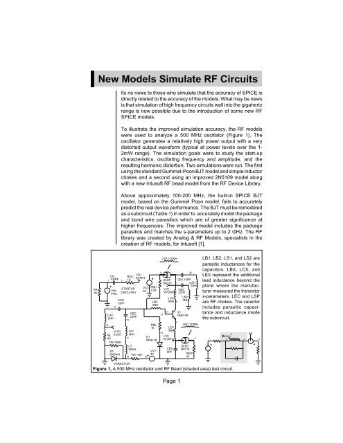
New Models Simulate RF Circuits - Intusoft
New Models Simulate RF Circuits - Intusoft
New Models Simulate RF Circuits - Intusoft

You also want an ePaper? Increase the reach of your titles
YUMPU automatically turns print PDFs into web optimized ePapers that Google loves.
<strong>New</strong> <strong>Models</strong> <strong>Simulate</strong> <strong>RF</strong> <strong>Circuits</strong><br />
Its no news to those who simulate that the accuracy of SPICE is<br />
directly related to the accuracy of the models. What may be news<br />
is that simulation of high frequency circuits well into the gigahertz<br />
range is now possible due to the introduction of some new <strong>RF</strong><br />
SPICE models.<br />
To illustrate the improved simulation accuracy, the <strong>RF</strong> models<br />
were used to analyze a 500 MHz oscillator (Figure 1). The<br />
oscillator generates a relatively high power output with a very<br />
distorted output waveform (typical at power levels over the 1-<br />
2mW range). The simulation goals were to study the start-up<br />
characteristics, oscillating frequency and amplitude, and the<br />
resulting harmonic distortion. Two simulations were run. The first<br />
using the standard Gummel-Poon BJT model and simple inductor<br />
chokes and a second using an improved 2N5109 model along<br />
with a new <strong>Intusoft</strong> <strong>RF</strong> bead model from the <strong>RF</strong> Device Library.<br />
Above approximately 100-200 MHz, the built-in SPICE BJT<br />
model, based on the Gummel Poon model, fails to accurately<br />
predict the real device performance. The BJT must be remodeled<br />
as a subcircuit (Table 1) in order to accurately model the package<br />
and bond wire parasitics which are of greater significance at<br />
higher frequencies. The improved model includes the package<br />
parasitics and matches the s-parameters up to 2 GHz. The <strong>RF</strong><br />
library was created by Analog & <strong>RF</strong> <strong>Models</strong>, specialists in the<br />
creation of <strong>RF</strong> models, for <strong>Intusoft</strong> [1].<br />
R3<br />
1K<br />
15<br />
CG<br />
1 100PF 2<br />
VIN<br />
PWL<br />
14<br />
LS2<br />
3NH<br />
CCO<br />
12PF<br />
V(15)<br />
RL VOUT<br />
50<br />
R2 10E6<br />
X2<br />
DN5441<br />
RGC<br />
1K<br />
STARTUP<br />
CIRCUITRY<br />
CBC<br />
22PF<br />
16<br />
LS1<br />
3NH<br />
17<br />
LT<br />
20NH<br />
V(3)<br />
START<br />
RTI 10K<br />
18 30<br />
VCC RBU<br />
8V 2.2K<br />
LBX<br />
3NH<br />
RBL<br />
1K<br />
D1<br />
DN4148<br />
VVT<br />
4V<br />
8<br />
13<br />
12<br />
LSP 170NH<br />
XLSP<br />
B9112<br />
V(7)<br />
VPOWER<br />
LCX<br />
5NH<br />
11<br />
LEX<br />
5NH<br />
V(3)<br />
START<br />
CEX<br />
5PF<br />
6<br />
X1<br />
QN5109<br />
5<br />
3<br />
22<br />
CB1 10PF<br />
7 9LB1<br />
3NH<br />
CB2<br />
47PF<br />
LB2<br />
3NH<br />
LEC 170NH<br />
XLEC<br />
B9112<br />
REX<br />
47<br />
4<br />
LB1, LB2, LS1, and LS2 are<br />
parasitic inductances for the<br />
capacitors. LBX, LCX, and<br />
LEX represent the additional<br />
lead inductance beyond the<br />
plane where the manufacturer<br />
measured the transistor<br />
s-parameters. LEC and LSP<br />
are <strong>RF</strong> chokes. The varactor<br />
includes parasitic capacitance<br />
and inductance inside<br />
the subcircuit.<br />
1 2 4<br />
3<br />
5<br />
VARACTOR<br />
Figure 1, A 500 MHz oscillator and <strong>RF</strong> Bead (shaded area) test circuit.<br />
Page 1
Modeling An <strong>RF</strong> Bead<br />
Although SPICE does contain a model for a nonlinear inductor it<br />
does not have a built-in bead model. Fortunately, one can be<br />
created using the a nonlinear magnetics model and passive<br />
elements. The new model, as shown in Figures 1 & 2, accurately<br />
simulates the impedance vs. frequency response and the change<br />
in impedance vs. temperature. The change in impedance with DC<br />
bias is also modeled due to the addition of the core model instead<br />
of a simple inductor. The bead model gives a very low DC<br />
impedance while providing a large impedance at higher frequencies.<br />
The model used here is for a ferrite bead made of a medium<br />
permeability nickel zinc material from Fair-Rite, P#2743009112.<br />
Other types of beads including beads on leads, wound beads and<br />
surface mount beads can be found in the <strong>RF</strong> library [2].<br />
180<br />
180<br />
1<br />
Z (2743003112) in Ohms<br />
140<br />
100.0<br />
60.0<br />
Z (2743009112) in Ohms<br />
140<br />
100.0<br />
60.0<br />
2<br />
3<br />
4<br />
20.0<br />
20.0<br />
1MEG 10MEG 100MEG 1G<br />
Impedance (Ohms) vs. Frequency in Hz<br />
Figure 2, The <strong>Intusoft</strong> <strong>RF</strong> Bead model simulates the proper impedance vs.<br />
frequency characteristics. The graph displays the response for several devices.<br />
Starting An Oscillator<br />
Simulation of oscillators present a variety of challenges, not the<br />
least of which is getting the oscillator to oscillate. When ISSPICE<br />
performs an AC or Transient analysis it first performs a DC<br />
analysis in order to establish the starting initial operating point for<br />
the circuit. If a stable operating point is found, which is the goal of<br />
the DC analysis, the oscillator may not oscillate during the<br />
transient (time domain) analysis unless some random disturbance<br />
is encountered.<br />
There are a number of ways to start an oscillator; each with<br />
varying results and consequences (Figure 3). The method chosen<br />
here was to introduce a voltage pulse into the circuit, specifically,<br />
at the emitter of the transistor (VIN 1 0 PWL...). Another<br />
possible method is to insert a current pulse somewhere in the<br />
resonant portion of the circuit, for example at LT (I1 18 17 PULSE<br />
.01 0). If the DC analysis does not converge, a sign that the circuit<br />
Page 2
Input Current Pulse At Time 0<br />
1<br />
Input Voltage Pulse<br />
4<br />
Ramping The Power Supply<br />
2<br />
UIC Transient Option<br />
No Starting Help Given<br />
3<br />
5<br />
5.0000N 15.000N 25.000N 35.000N 45.000N<br />
TIME in Secs<br />
Figure 3, Comparison of the various methods of “thumping” an oscillator to get it<br />
started show a current pulse at LT to be the most effective for this circuit.<br />
is unstable and may want to oscillate without any help, the UIC<br />
keyword can be issued in the .TRAN statement. For example,<br />
.TRAN .1NS 50NS UIC. This will cause the simulation to proceed<br />
directly to the Transient analysis bypassing the DC analysis. The<br />
.IC and “IC=” parameters can then be used to set initial transient<br />
conditions and unbalance the oscillator. One problem with using<br />
UIC is that no DC operating point will be produced inhibiting study<br />
of the circuit bias. The last method is similar to the first and<br />
involves ramping of the power supply (VCC 8 0 PULSE 0 8V 0<br />
5NS). This method may not work well, however, due to the bypass<br />
capacitors. In general, when ramping a source, make sure to give<br />
the ramp a realistic slope in order to avoid “timestep too small”<br />
errors. The first two methods are the most often recommended as<br />
the other methods may not work or may introduce transient startup<br />
residues [3].<br />
Circuit Modeling<br />
The oscillator circuit was first simulated with two inductor chokes,<br />
LSP and LEC (Figure 1), and a standard .MODEL statement for<br />
the 2N5109 transistor. In SPICE, the standard representation for<br />
a transistor uses the Gummel-Poon model. Various parameters<br />
in the SPICE .MODEL statement are altered in order to cause the<br />
“generic nature” of the Gummel-Poon template to represent a<br />
particular device.<br />
In a second simulation, the chokes were each replaced with the<br />
new <strong>RF</strong> bead model. The simple transistor model was replaced<br />
with a subcircuit representation. Since the Gummel-Poon model<br />
can not adequately represent BJT behavior above approximately<br />
200MegHz, a composite model must be assembled. The SPICE<br />
subcircuit, containing a BJT model and various parasitic elements,<br />
is utilized for this purpose.<br />
Page 3
When simulating in SPICE it is best to use a subcircuit representation<br />
for a device rather than forcing model parameters to have<br />
unreasonable values. If model parameters are used outside their<br />
physical bounds, the model may work well in one area, but<br />
incorrectly in another. For example, the device may behave<br />
properly during the AC small signal analysis, but poorly during the<br />
nonlinear transient analysis. Some vendors who produce SPICE<br />
model use this approach and the user should beware. <strong>Models</strong> for<br />
<strong>RF</strong> transistors that are going to be used for both linear and<br />
nonlinear analysis can not be produced this way. A subcircuit<br />
representation must be used!<br />
Note: Parasitics for the passive elements were maintained for<br />
both simulation cases.<br />
1.000<br />
14.69<br />
0<br />
12.69<br />
VOUT in Volts<br />
-1.000<br />
-2.000<br />
VPOWER in Volts<br />
10.69<br />
8.690<br />
1<br />
2<br />
-3.000<br />
6.690<br />
5.000N 15.00N 25.00N 35.00N 45.00N<br />
WFM.2 VPOWER vs. TIME in Secs<br />
With Bead and Parasitics<br />
11.81<br />
1.000<br />
1<br />
9.811<br />
0<br />
VPOWER in Volts<br />
7.811<br />
5.811<br />
VOUT in Volts<br />
-1.000<br />
-2.000<br />
3.811<br />
-3.000<br />
2<br />
5.000N 15.00N 25.00N 35.00N 45.00N<br />
WFM.1 VOUT vs. TIME in Secs<br />
No Beads with Parasitics<br />
Figure 4, Comparison of the start-up and power supply waveforms with (Top) and<br />
without (Bottom) the new <strong>RF</strong> bead model.<br />
Page 4
Results<br />
In order to isolate VCC and not contaminate the power supply with<br />
the 500 MHz oscillating waveform, adequate bypassing is required.<br />
A voltage generator represents a perfect bypass because<br />
it is zero ohms at all frequencies. This is quite different from the<br />
real world.<br />
As shown in Figure 4, use of an inductor causes a droop in the<br />
VCC voltage. The reason for the droop is that the 170nH represents<br />
a large impedance. As the oscillator starts up, the transistor<br />
wants more current. Because of the large inductance it can't draw<br />
adequate current so it starts to discharge the bypass capacitors.<br />
This appears as a drooping in the VCC power (lower graph). The<br />
bead, on the other hand, has a very low DC impedance and a high<br />
AC impedance. By choosing the proper bead, a frequency response<br />
can be selected that will block all the AC around the<br />
oscillation frequency. With the bead (upper graph), the VCC line<br />
doesn't droop and shows that the size of the ripple stays the same<br />
revealing the imperfections in the bypassing. Also note that the<br />
oscillation starts slower and does not have quite as much power<br />
out with the bead inserted (to be expected) as it does when the<br />
inductors are used.<br />
The oscillator with no BJT parasitics or beads still oscillates<br />
because it was made to be tolerant of package parasitics, but the<br />
results predicted were inaccurate in several important areas. As<br />
shown in Figure 5, the FFT and transient response of the circuit<br />
with beads and new <strong>RF</strong> BJT subcircuit model reveals that the<br />
frequency of oscillation is lower and the distortion higher.<br />
Conclusions<br />
From the simulations performed, it is clear that modeling the<br />
proper circuit parasitics is of vital importance, especially at <strong>RF</strong><br />
frequencies. It is recommended that initial simulations run for<br />
many cycles in order to verify that stable oscillation is actually<br />
taking place. As for performing an FFT, the ISSPICE .TRAN tstart<br />
parameter can be used to delay the start of data taking until steady<br />
state oscillation has been reached.<br />
With the new bead and BJT models in the <strong>RF</strong> library, ISSPICE is<br />
able to show the peak component stresses when power is<br />
applied, the transient start-up performance, and the variations in<br />
the power supply. In contrast to the linear analysis programs<br />
commonly used by <strong>RF</strong> designers, ISSPICE simulations can reveal<br />
many important circuit properties such as efficiency, power dissipation,<br />
start up characteristics, and harmonic distortion. Characteristics<br />
that would be either difficult or impossible to measure.<br />
Page 5
FFT of VOUT (NBNP) in Volts<br />
1.600<br />
1.200<br />
800.0M<br />
400.0M<br />
FFT of VOUT (WBWP) in Volts<br />
800.0M<br />
600.0M<br />
400.0M<br />
200.0M<br />
With<br />
Beads and<br />
BJT<br />
Parasitics<br />
x<br />
<<br />
519.5MEG<br />
733.3M<br />
><br />
With<br />
Inductors<br />
and No<br />
Parasitics<br />
x<br />
<<br />
1.052G<br />
135.4M<br />
><br />
0<br />
0<br />
1<br />
2<br />
200.0MEG 600.0MEG 1.000G 1.400G 1.800G<br />
WFM.2 VOUT vs. TIME in Secs<br />
FFT Responses<br />
dx = 532.8MEG dy = -597.9M<br />
3.000<br />
1.000<br />
With Beads and BJT<br />
Parasitics<br />
1<br />
VOUT (WBWP) in Volts<br />
2.000<br />
1.000<br />
0<br />
-1.000<br />
VOUT (NBNP) in Volts<br />
0<br />
-1.000<br />
-2.000<br />
-3.000<br />
With Inductors and<br />
No Parasitics<br />
2<br />
91.00N 93.00N 95.00N 97.00N 99.00N<br />
TIME in Secs<br />
Output Waveforms at Steady State<br />
Figure 5, Comparison of the frequency spectrum and time waveforms using the new<br />
<strong>Intusoft</strong> BJT and bead models vs. the Gummel-Poon model and inductor chokes. The<br />
new models give a more accurate prediction of distortion and oscillation frequency.<br />
Table 1, ISSPICE Subcircuit for an <strong>RF</strong> Transistor & Bead<br />
1<br />
.SUBCKT QN5109 1 2 3<br />
LC 1 4 0.875E-9<br />
LC<br />
4<br />
LB 2 6 1.590E-9<br />
CB CC<br />
LE 5 3 2.650E-9<br />
2 LB 6<br />
CC 4 3 1.410E-12<br />
Q1<br />
CB 4 6 0.561E-12<br />
LE<br />
5 3<br />
Q1 4 6 5 QR33<br />
.MODEL QR33 NPN ( BF=44 VAF=160 VAR=16.0 RC=0.69<br />
+RB=1.57 RE=2.75 IKF=0.28E+00 ISE=0.36E-13 TF=0.111E-09<br />
+TR=0.80E-08 ITF=0.82E-01 VTF=0.66E+01 CJC=2.758E-12<br />
+CJE=1.822E-12 XTI=3.0 NE=1.5 ISC=0.12E-13 EG=1.11<br />
+XTB=1.5 BR=1.14 VJC=0.75 VJE=0.75 IS=0.40E-14<br />
+MJC=0.33 MJE=0.33 XTF=4.0 IKR=0.28E+00 KF=0.1E-14<br />
+NC=1.7 FC=0.50 RBM=1.1 IRB=0.40E-01 XCJC=0.5 )<br />
.ENDS<br />
.SUBCKT BEAD 1 2<br />
R4 1 2 220 TC=-.00333<br />
C2 1 2 .9PF<br />
RX 3 2 1E12<br />
CB 3 2 7.432N<br />
F1 1 2 VM1 1<br />
G2 2 3 1 2 1<br />
.MODEL DCLAMP D<br />
E1 4 2 3 2 1<br />
+CJO=8.2286P VJ=25<br />
VM1 4 5<br />
.ENDS<br />
RB 5 2 341.5<br />
RS 5 6 3.7904<br />
VP 7 2 300<br />
D1 6 7 DCLAMP<br />
VN 2 8 300<br />
D2 8 6 DCLAMP<br />
Page 6
References<br />
[1] Analog & <strong>RF</strong> <strong>Models</strong>, Bill Sands (602) 575-5323, FAX (602)<br />
297-5160<br />
[2] <strong>RF</strong> Device Library, <strong>Intusoft</strong>, 1990<br />
[3] “SIMULATING WITH SPICE”, L.G. Meares, C.E. Hymowtiz, <strong>Intusoft</strong>,<br />
1988<br />
Page 7