Download HSP45102 12 Bit NCO Data Sheet
Download HSP45102 12 Bit NCO Data Sheet
Download HSP45102 12 Bit NCO Data Sheet

Create successful ePaper yourself
Turn your PDF publications into a flip-book with our unique Google optimized e-Paper software.
<strong>HSP45102</strong><br />
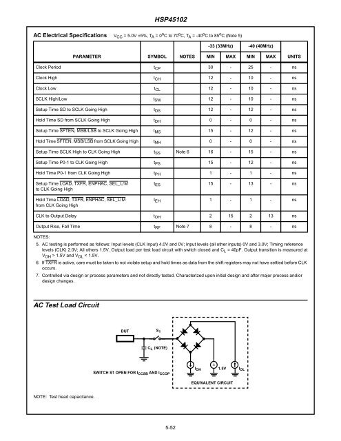
AC Electrical Specifications V CC = 5.0V ±5%, T A = 0 o C to 70 o C, T A = -40 o C to 85 o C (Note 5)<br />
-33 (33MHz) -40 (40MHz)<br />
PARAMETER SYMBOL NOTES<br />
MIN MAX MIN MAX<br />
UNITS<br />
Clock Period t CP 30 - 25 - ns<br />
Clock High t CH <strong>12</strong> - 10 - ns<br />
Clock Low t CL <strong>12</strong> - 10 - ns<br />
SCLK High/Low t SW <strong>12</strong> - 10 - ns<br />
Setup Time SD to SCLK Going High t DS <strong>12</strong> - <strong>12</strong> - ns<br />
Hold Time SD from SCLK Going High t DH 0 - 0 - ns<br />
Setup Time SFTEN, MSB/LSB to SCLK Going High t MS 15 - <strong>12</strong> - ns<br />
Hold Time SFTEN, MSB/LSB from SCLK Going High t MH 0 - 0 - ns<br />
Setup Time SCLK High to CLK Going High t SS Note 6 16 - 15 - ns<br />
Setup Time P0-1 to CLK Going High t PS 15 - <strong>12</strong> - ns<br />
Hold Time P0-1 from CLK Going High t PH 1 - 1 - ns<br />
Setup Time LOAD, TXFR, ENPHAC, SEL_L/M<br />
to CLK Going High<br />
Hold Time LOAD, TXFR, ENPHAC, SEL_L/M<br />
from CLK Going High<br />
t ES 15 - 13 - ns<br />
t EH 1 - 1 - ns<br />
CLK to Output Delay t OH 2 15 2 13 ns<br />
Output Rise, Fall Time t RF Note 7 8 - 8 - ns<br />
NOTES:<br />
5. AC testing is performed as follows: Input levels (CLK Input) 4.0V and 0V; Input levels (all other inputs) 0V and 3.0V; Timing reference<br />
levels (CLK) 2.0V; All others 1.5V. Output load per test load circuit with switch closed and C L = 40pF. Output transition is measured at<br />
V OH > 1.5V and V OL < 1.5V.<br />
6. If TXFR is active, care must be taken to not violate setup and hold times as data from the shift registers may not have settled before CLK<br />
occurs.<br />
7. Controlled via design or process parameters and not directly tested. Characterized upon initial design and after major process and/or<br />
design changes.<br />
AC Test Load Circuit<br />
DUT<br />
S 1<br />
±<br />
C L (NOTE)<br />
SWITCH S1 OPEN FOR I CCSB AND I CCOP<br />
I OH 1.5V I OL<br />
EQUIVALENT CIRCUIT<br />
NOTE: Test head capacitance.<br />
5-52