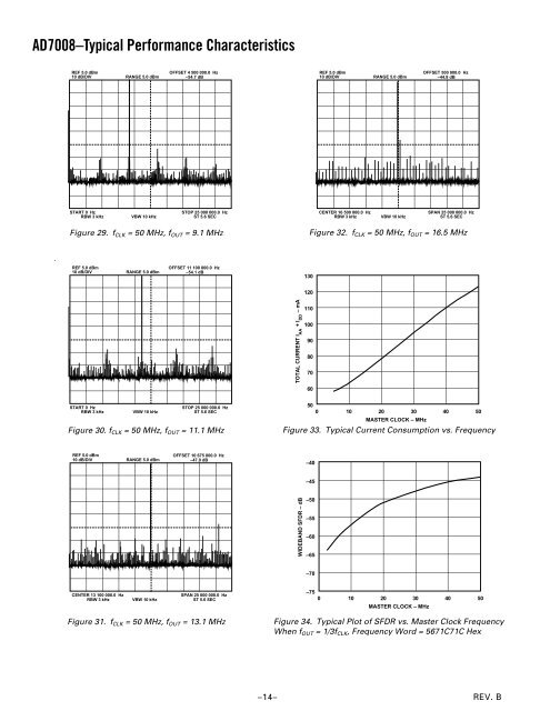
<strong>AD7008</strong>–Typical Performance CharacteristicsREF 5.0 dBm10 dB/DIV RANGE 5.0 dBmOFFSET 4 500 000.0 Hz–54.7 dBREF 5.0 dBm10 dB/DIV RANGE 5.0 dBmOFFSET 500 000.0 Hz–44.8 dBSTART 0 HzRBW 3 kHzVBW 10 kHzSTOP 25 000 000.0 HzST 5.6 SECCENTER 16 500 000.0 HzRBW 3 kHzVBW 10 kHzSPAN 25 000 000.0 HzST 5.6 SECFigure 29. f CLK = 50 MHz, f OUT = 9.1 MHzFigure 32. f CLK = 50 MHz, f OUT = 16.5 MHzREF 5.0 dBm10 dB/DIV RANGE 5.0 dBmOFFSET 11 100 000.0 Hz–54.1 dB130120TOTAL CURRENT I AA+ I DD– mA11010090807060START 0 HzRBW 3 kHzVBW 10 kHzSTOP 25 000 000.0 HzST 5.6 SECFigure 30. f CLK = 50 MHz, f OUT = 11.1 MHz50010 20 30 40 50MASTER CLOCK – MHzFigure 33. Typical Current Consumption vs. FrequencyREF 5.0 dBm10 dB/DIV RANGE 5.0 dBmOFFSET 10 675 000.0 Hz–47.0 dB–40–45WIDEBAND SFDR – dB–50–55–60–65–70CENTER 13 100 000.0 HzRBW 3 kHzVBW 10 kHzSPAN 25 000 000.0 HzST 5.6 SEC–750102030MASTER CLOCK – MHz4050Figure 31. f CLK = 50 MHz, f OUT = 13.1 MHzFigure 34. Typical Plot of SFDR vs. Master Clock FrequencyWhen f OUT = 1/3f CLK , Frequency Word = 5671C71C Hex–14–REV. B
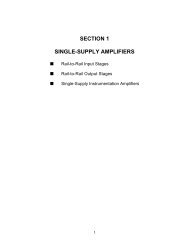
<strong>AD7008</strong><strong>AD7008</strong>/PCB <strong>DDS</strong> EVALUATION BOARDThe <strong>AD7008</strong>/PCB <strong>DDS</strong> Evaluation Board allows designers toevaluate the high performance <strong>AD7008</strong> <strong>DDS</strong> <strong>Modulator</strong> with aminimum amount of effort.To prove this <strong>DDS</strong> will meet the user’s waveform synthesis requirements,the only things needed are the <strong>AD7008</strong>/PCB <strong>DDS</strong>Evaluation Board, +5 V power supply, an IBM-compatible PC,and a spectrum analyzer. The evaluation setup is shown below.The <strong>DDS</strong> evaluation kit includes a populated, tested <strong>AD7008</strong>/PCB board; software which controls the <strong>AD7008</strong> through theparallel printer port in a DOS or Windows environment and an<strong>AD7008</strong>P.The <strong>AD7008</strong> direct digital synthesis chip is a numericallycontrolled oscillator employing a 32-bit phase accumulator, sineand cosine look-up tables, and a l0-bit D/A converter integratedon a single <strong>CMOS</strong> chip. Modulation capabilities are providedfor phase modulation, frequency modulation, and both in-phaseand quadrature amplitude modulation suitable for SSBgeneration.Clock rates up to 20 MHz and 50 MHz are supported. Frequencyaccuracy can be controlled to one part in four billion.OPTIONALTTL CLOCKREFERENCEGENERATORSTANDARDPRINTERCABLESOFTWAREPROVIDEDCLOCKOSCILLATORINTERFACELOGICIBM-COMPATIBLE PC<strong>AD7008</strong>50MHz<strong>CMOS</strong> <strong>DDS</strong>POWERSUPPLYINTERFACE<strong>AD7008</strong> <strong>DDS</strong> EVALUATION BOARD50Ω CABLESPECTRUM ANALYZEREXTERNALPOWERSUPPLYFigure 35. <strong>AD7008</strong> <strong>DDS</strong> Evaluation Board SetupTable IV. <strong>AD7008</strong>/PCB Typical Electrical Characteristics(Nominal power supplies, CLK = 50 MHz)TypicalCharacteristics Value Units+5.0 V Supply Current 125 mA<strong>AD7008</strong> Output Voltage 0 to +1.0 V(Terminated into 50 Ω Externally)<strong>CMOS</strong> clock input HIGH 4.1 to 5 V<strong>CMOS</strong> clock input LOW 0.0 to 0.5 VUSING THE <strong>AD7008</strong>/PCB <strong>DDS</strong> EVALUATION BOARDThe <strong>AD7008</strong>/PCB evaluation kit is a test system designed tosimplify the evaluation of the <strong>AD7008</strong> 50 MHz Direct DigitalSynthesizer. Provisions to control the <strong>AD7008</strong> from the printerport of an IBM-compatible PC are included, along with the+5Vnecessary software. This data sheet provides information onoperating the evaluation board; additional details are availablefrom the ADI technical assistance line 1-800-ANALOGD.Prototyping AreaAn area near one edge of the board is intentionally left void ofcomponents to allow the user to add additional circuits to theevaluation test set. Users may want to build custom analog filtersfor the outputs, or add buffers and operational amplifiersused in the final applications.XO vs. External ClockThe reference clock of the <strong>AD7008</strong>/PCB is normally providedby a 50 MHz <strong>CMOS</strong> oscillator. This oscillator can be removedand an external <strong>CMOS</strong> clock connected to CLOCK. If an externalclock is used, a 50 Ω resistor R6 should be installed.Power SupplyPower for the <strong>AD7008</strong>/PCB must be provided externallythrough the pin connections, as described in the Inputs/Outputs.The power leads should be twisted to reduce ground loops.<strong>AD7008</strong>/PCB BILL OF MATERIALQuantity Reference Description1 C1 Tag – Tant Cap, 10 µF, 35 V, 20%8 C2–C9 Cer Chip Cap, 0.1 µF, MurataGrm426 CLOCK, FSEL SMB – Submin Snap-on (Male)I OUT , I OUTN PCB MT PlugSCLK, SDATA1 FSADJ RN55 – Res Met Film, 3921 LK1 HDR SIP 3-Pin Male1 Shunt 530153-21 P1 36-Pin D Conn Rt Ang PcmtFem AMP1 P2 PC Voltage Ter Blk w/ScrewsAugat RDI3 R1–R3 RN55 – Res Met Film, 10k2 R4, R5 RN55 – Res Met Film, 49.91 RZ1 10P Bussed Res Ntwk, 10kCSC10A01103G1 RZ2 6P Bussed Res Ntwk, 4.7kCSC06A01472G1 U1 <strong>AD7008</strong> JP50 <strong>CMOS</strong> <strong>DDS</strong><strong>Modulator</strong>1 U2 74HC74 – Dual D-type Pos-Ed-Trigd Flip-Flop1 V REF Pin Terminal, Testpoint1 XTAL OSC XTAL, Fox F1100H50 MHz1 Socket, Methode 213-044-5014 Support, Nylon1 PCB, 48295(-)26 Pin Sockets, Closed EndREV. B –15–