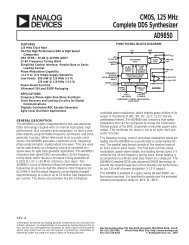
AD7008 CMOS DDS Modulator
AD7008 CMOS DDS Modulator
AD7008 CMOS DDS Modulator
You also want an ePaper? Increase the reach of your titles
YUMPU automatically turns print PDFs into web optimized ePapers that Google loves.
<strong>AD7008</strong>Table I. Latency TableLatencyFunction (Synchronizer Enabled CR3 = 0 1 )FSelect 14t 1Phase 13t 1IQ Mod 11t 1NOTE1 All latencies are reduced by 4t 1 when CR3 = 1 (synchronizer disabled). 1t 1 isequal to one pipeline delay.Table II. Source and Destination RegisterTC3 TC2 TC1 TC0 LOAD Source Register Destination RegisterX X X X 0 N/A N/A0 0 X X 1 Parallel COMMAND*1 0 0 0 1 Parallel FREQ01 0 0 1 1 Parallel FREQ11 0 1 0 1 Parallel PHASE1 0 1 1 1 Parallel IQMOD1 1 0 0 1 Serial FREQ01 1 0 1 1 Serial FREQ11 1 1 0 1 Serial PHASE1 1 1 1 1 Serial IQMOD*The Command Register can only be loaded from the parallel assembly registers.Table III. <strong>AD7008</strong> Control RegistersRegister Size Reset State DescriptionCOMMAND REG* 4 Bits CR3–CR0 All Zeros Command Register. This is written to using the parallel assembly register.FREQ0 REG 32 Bits DB31–DB0 All Zeros Frequency Register 0. This defines the output frequency, whenFSELECT = 0, as a fraction of the CLOCK frequency.FREQ1 REG 32 Bits DB31–DB0 All Zeros Frequency Register 1. This defines the output frequency, whenFSELECT = 1, as a fraction of the CLOCK frequency.PHASE REG 12 Bits DB11–DB0 All Zeros Phase Offset Register. The contents of this register is added to theoutput of the phase accumulator.IQMOD REG 20 Bits DB19–DB0 All Zeros I and Q Amplitude Modulation Register. This defines the amplitude ofthe I and Q signals as 10-bit twos complement binary fractions.DB[19:10] is multiplied by the Quadrature (sine component andmultiplied by the In-Phase (cosine) component.*On power up, the Command Register should be configured by the user for the desired mode before operation.Table IV. Command Register Bits*CR0 = 0 Eight-Bit Databus. Pins D15–D8 are ignored and the parallel assembly register shifts eight places left on each write.Hence four successive writes are required to load the 32-bit parallel assembly register, Figure 6.= 1 Sixteen-Bit Databus. The parallel assembly register shifts 16 places left on each write. Hence two successive writes arerequired to load the 32-bit parallel assembly register, Figure 5.CR1 = 0 Normal Operation.= 1 Low Power Sleep Mode. Internal Clocks and the DAC current sources are turned off.CR2 = 0 Amplitude Modulation Bypass. The output of the sine LUT is directly sent to the DAC.= 1 Amplitude Modulation Enable. IQ modulation is enabled allowing AM or QAM to be performed.CR3 = 0 Synchronizer Logic Enabled. The FSELECT, LOAD and TC3–TC0 signals are passed through a 4-stage pipelineto synchronize them with the CLOCK, avoiding metastability problems.= 1 Synchronizer Logic Disabled. The FSELECT, LOAD and TC3–TC0 signals bypass the synchronization logic. Thisallows for faster response to the control signals.*The Command Register can only be loaded from the parallel assembly register.REV. B –7–


