AD7008 CMOS DDS Modulator
AD7008 CMOS DDS Modulator
AD7008 CMOS DDS Modulator

You also want an ePaper? Increase the reach of your titles
YUMPU automatically turns print PDFs into web optimized ePapers that Google loves.
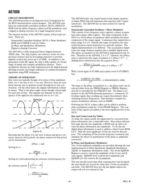
<strong>AD7008</strong>CIRCUIT DESCRIPTIONThe <strong>AD7008</strong> provides an exciting new level of integration forthe RF/Communications system designer. The <strong>AD7008</strong> combinesthe numerically controlled oscillator (NCO), SINE/CO-SINE look-up tables, frequency, phase and IQ modulators, anda digital-to-analog converter on a single integrated circuit.The internal circuitry of the <strong>AD7008</strong> consists of four main sections.These are:Numerically Controlled Oscillator (NCO) + Phase <strong>Modulator</strong>SINE and COSINE Look-Up TablesIn Phase and Quadrature <strong>Modulator</strong>sDigital-to-Analog ConverterThe <strong>AD7008</strong> is a fully integrated Direct Digital Synthesis(<strong>DDS</strong>) chip. The chip requires one reference clock, two lowprecisionresistors and six decoupling capacitors to providedigitally created sine waves up to 25 MHz. In addition to thegeneration of this RF signal, the chip is fully capable of a broadrange of simple and complex modulation schemes. Thesemodulation schemes are fully implemented in the digital domainallowing accurate and simple realization of complex modulationalgorithms using DSP techniques.THEORY OF OPERATIONSine waves are typically thought of in terms of their amplitudeform: a(t) = sin (ωt) or a(t) = cos (ωt). However, these are nonlinearand not easy to generate except through piece wise construction.On the other hand, the angular information is linearin nature. That is, the phase angle rotates though a fixed anglefor each unit of time. The angular rate depends on the frequencyof the signal by the traditional rate of: ω = 2 πf.+10–12π0MAGNITUDEPHASEFigure 9.Knowing that the phase of a sine wave is linear and given a referenceinterval (clock period), the phase rotation for that periodcan be determined.Solving for w:∆Phase =ωdtω= ∆Phasedt= 2 πfSolving for f and substituting the reference clock frequency for⎛the reference period: ⎜⎝1f CLOCK⎞= dt⎟:⎠The <strong>AD7008</strong> builds the output based on this simple equation.A simple <strong>DDS</strong> chip will implement this equation with 3 majorsubcircuits. The <strong>AD7008</strong> has an extra section for I and Qmodulation.Numerically Controlled Oscillator + Phase <strong>Modulator</strong>This consists of two frequency select registers, a phase accumulatorand a phase offset register. The main component of theNCO is a 32-bit phase accumulator which assembles the phasecomponent of the output signal. Continuous time signals have aphase range 0 to 2 π. Outside this range of numbers, the sinusoidalfunctions repeat themselves in a periodic manner. Thedigital implementation is no different. The accumulator simplyscales the range of phase numbers into a multibit digital word.The phase accumulator in the <strong>AD7008</strong> is implemented with 32bits. Therefore in the <strong>AD7008</strong>, 2 π = 2 32 . Likewise, the ∆Phaseterm is scaled into this range of numbers 0 ≤ ∆Phase ≤ 2 32 – 1.Making these substitutions into the equation above:f = ∆Phase × f CLOCK2 32 where 0 ≤∆Phase < 2 32With a clock signal of 50 MHz and a phase word of 051EB852hex:f =51EB852 × 50 MHz2 32 = 1.000000000931 MHzThe input to the phase accumulator (i.e., the phase step) can beselected either from the FREQ0 Register or FREQ1 Register,and this is controlled by the FSELECT pin. The phase accumulatorin the <strong>AD7008</strong> inherently generates a continuous 32-bit phase signal, thus avoiding any output discontinuity whenswitching between frequencies. This facilitates complex frequencymodulation schemes, such as GMSK.Following the NCO, a phase offset can be added to performphase modulation using the 12-bit PHASE Register. The contentsof this register are added to the most significant bits of theNCO.Sine and Cosine Look-Up TablesTo make the output useful, the signal must be converted fromphase information into a sinusoidal value. Since phase informationmaps directly into amplitude, a ROM look up table convertsthe phase information into amplitude. To do this thedigital phase information is used to address a Sine/Cosine ROMLUT. Only the most significant 12 bits are used for this purpose.The remaining 20 bits provide frequency resolution andminimize the effects of quantization of the phase to amplitudeconversion.In Phase and Quadrature <strong>Modulator</strong>sTwo 10-bit amplitude multipliers are provided allowing the easyimplementation of either Quadrature Amplitude Modulation(QAM) or Amplitude Modulation (AM). The 20-bit IQMODRegister is used to control the amplitude of the I (cos) and Q(sin) signals. IQMOD [9:0] controls the I amplitude andIQMOD [19:10] controls the Q amplitude.The user should ensure that when summing the I and Q signalsthe sum should not exceed the value that a 10-bit accumulatorcan hold. The <strong>AD7008</strong> does not clip the digital output; theoutput will roll over instead of clip.f = ∆Phase × f CLOCK2 π–8–REV. B