Microcontroller Solutions TechZone Magazine, April 2011 - Digikey
Microcontroller Solutions TechZone Magazine, April 2011 - Digikey
Microcontroller Solutions TechZone Magazine, April 2011 - Digikey

You also want an ePaper? Increase the reach of your titles
YUMPU automatically turns print PDFs into web optimized ePapers that Google loves.
As shown in Figure 1, a typical 16-bit parallel fl ash memory delivers a<br />
data transfer rate of 20 Megabytes per second. In systems that use<br />
a 32-bit microcontroller with a 32-bit bus for the external memory<br />
(like those from NXP), the designer can opt to use two 16-bit parallel<br />
devices in combination for a rate of 40 Megabytes per second.<br />
However, the added speed comes at a cost. The confi guration uses<br />
two separate parallel fl ash memories, each housed in a package<br />
with dozens of pins, and that may be more, in terms of package<br />
size, pin count, and PCB space, than the designer can afford.<br />
Serial fl ash, which typically uses the simple four-pin Serial<br />
Peripheral Interface (SPI), can be a good alternative to parallel<br />
fl ash when space, power, and cost are concerns, but it’s much<br />
slower. Figure 1 shows that a typical SPI fl ash operating at 50<br />
MHz transfers data at roughly 5 Megabytes per second (eight<br />
times slower than a confi guration that uses two 16-bit parallel<br />
devices). Another consideration is that the SPI interface on most<br />
microcontrollers is connected to the MCU’s peripheral matrix, where<br />
data has to be received by driver code and put into on-board RAM<br />
before the processor can access it. This can slow things down,<br />
since each read from serial fl ash has to go through an SPI software<br />
layer. Depending on the application, using the standard SPI interface<br />
for external memory may not be fast enough.<br />
The new Quad SPI fl ash format, which uses a modifi ed, six-pin SPI<br />
confi guration, is much faster than traditional SPI formats. As shown<br />
in Figure 1, Quad SPI delivers a transfer rate of 40 Megabytes per<br />
second, which is the same as using two 16-bit parallel devices.<br />
Using Quad SPI is often much less expensive than the parallel<br />
approach, since it uses far fewer pins and a much smaller package.<br />
It would seem that Quad SPI fl ash would be a good replacement for<br />
parallel fl ash in embedded systems, but the reality is that today’s<br />
32-bit microcontrollers aren’t designed to support Quad SPI fl ash<br />
at its maximum speeds. This is because the Quad SPI interface, like<br />
the traditional SPI interface, is connected to the microcontroller’s<br />
peripheral matrix.<br />
Eliminating the tradeoff<br />
NXP has developed a new peripheral function, called the SPI<br />
Flash Interface (SPIFI) that essentially eliminates the parallel/<br />
serial tradeoff. The patent-pending SPIFI (“spiffy”) peripheral lets<br />
low-cost SPI and new Quad SPI fl ash memories appear in the<br />
memory map of an ARM Cortex-M3 microcontroller, so the MCU<br />
can use external SPI fl ash with only a minimal performance penalty<br />
compared to external parallel fl ash memories. The complete<br />
memory space of the external SPI fl ash appears in the MCU’s<br />
memory map, so the microcontroller can access the external<br />
memory directly, without a software API or library.<br />
When used with a Quad SPI fl ash, for example, the SPIFI peripheral<br />
supports a data transfer rate of up to 40 Megabytes per second.<br />
The designer can choose a less expensive SPI fl ash device, with<br />
its compact footprint and simple confi guration, but doesn’t have<br />
to sacrifi ce performance. The designer may also be able to choose<br />
a smaller, less costly microcontroller, because the system won’t<br />
need a bulky interface for external parallel memory. The SPIFI<br />
peripheral enables an embedded system that makes better use<br />
of memory resources yet remains compact and effi cient while<br />
lowering overall cost.<br />
The SPIFI peripheral is a dedicated function that will initially<br />
be available on the NXP LPC1800 series of ARM Cortex-M3<br />
microcontrollers. It will also be available on upcoming product lines,<br />
including the low-cost Cortex-M0 series and the Cortex M4 line of<br />
digital serial controllers (DSCs).<br />
SPIFI supports most serial fl ash devices on the market today<br />
(including those with quad read/write capability) and is designed<br />
for easy confi guration and programming. It uses four or six pins<br />
(depending on the type of serial fl ash used), works with a small<br />
register set, is optimized for effi cient memory transactions, and<br />
uses software commands that reduce CPU overhead and streamline<br />
memory interactions.<br />
How SPIFI works<br />
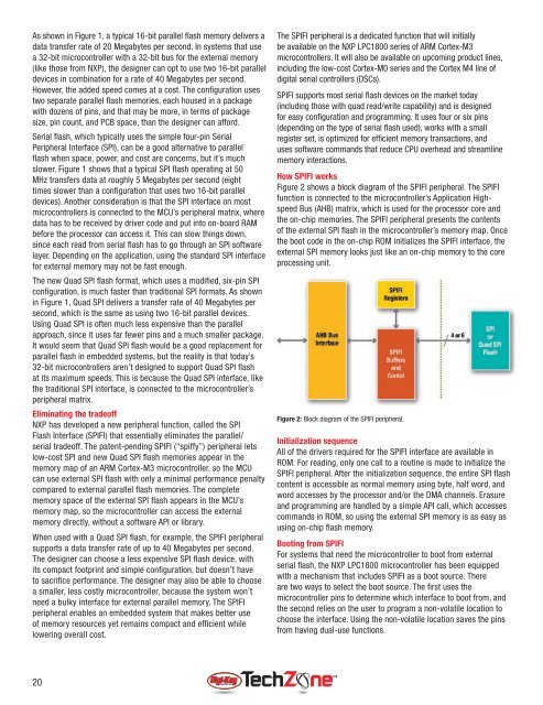
Figure 2 shows a block diagram of the SPIFI peripheral. The SPIFI<br />
function is connected to the microcontroller’s Application Highspeed<br />
Bus (AHB) matrix, which is used for the processor core and<br />
the on-chip memories. The SPIFI peripheral presents the contents<br />
of the external SPI fl ash in the microcontroller’s memory map. Once<br />
the boot code in the on-chip ROM initializes the SPIFI interface, the<br />
external SPI memory looks just like an on-chip memory to the core<br />
processing unit.<br />
Figure 2: Block diagram of the SPIFI peripheral.<br />
Initialization sequence<br />
All of the drivers required for the SPIFI interface are available in<br />
ROM. For reading, only one call to a routine is made to initialize the<br />
SPIFI peripheral. After the initialization sequence, the entire SPI fl ash<br />
content is accessible as normal memory using byte, half word, and<br />
word accesses by the processor and/or the DMA channels. Erasure<br />
and programming are handled by a simple API call, which accesses<br />
commands in ROM, so using the external SPI memory is as easy as<br />
using on-chip fl ash memory.<br />
Booting from SPIFI<br />
For systems that need the microcontroller to boot from external<br />
serial fl ash, the NXP LPC1800 microcontroller has been equipped<br />
with a mechanism that includes SPIFI as a boot source. There<br />
are two ways to select the boot source. The fi rst uses the<br />
microcontroller pins to determine which interface to boot from, and<br />
the second relies on the user to program a non-volatile location to<br />
choose the interface. Using the non-volatile location saves the pins<br />
from having dual-use functions.<br />
20