Journal of Applied Science Studies - Ozean Publications
Journal of Applied Science Studies - Ozean Publications
Journal of Applied Science Studies - Ozean Publications

You also want an ePaper? Increase the reach of your titles
YUMPU automatically turns print PDFs into web optimized ePapers that Google loves.
<strong>Ozean</strong> <strong>Journal</strong> <strong>of</strong> <strong>Applied</strong> <strong>Science</strong>s 1(1), 2008<br />
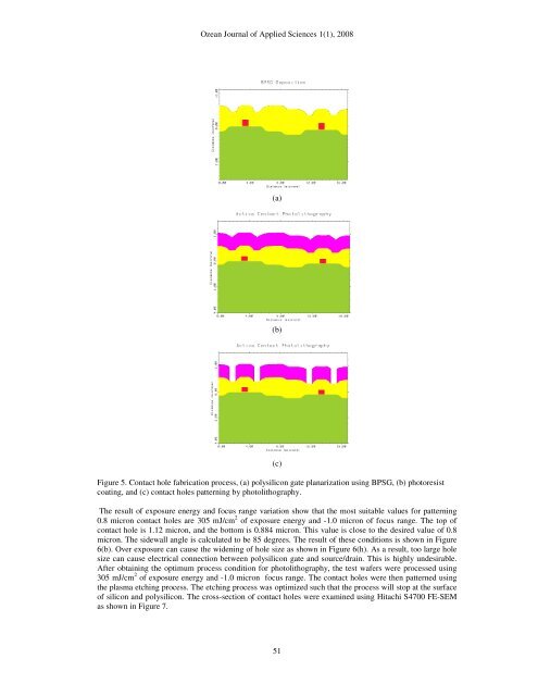
(a)<br />
(b)<br />
Figure 5. Contact hole fabrication process, (a) polysilicon gate planarization using BPSG, (b) photoresist<br />
coating, and (c) contact holes patterning by photolithography.<br />
(c)<br />
The result <strong>of</strong> exposure energy and focus range variation show that the most suitable values for patterning<br />
0.8 micron contact holes are 305 mJ/cm 2 <strong>of</strong> exposure energy and -1.0 micron <strong>of</strong> focus range. The top <strong>of</strong><br />
contact hole is 1.12 micron, and the bottom is 0.884 micron. This value is close to the desired value <strong>of</strong> 0.8<br />
micron. The sidewall angle is calculated to be 85 degrees. The result <strong>of</strong> these conditions is shown in Figure<br />
6(b). Over exposure can cause the widening <strong>of</strong> hole size as shown in Figure 6(h). As a result, too large hole<br />
size can cause electrical connection between polysilicon gate and source/drain. This is highly undesirable.<br />
After obtaining the optimum process condition for photolithography, the test wafers were processed using<br />
305 mJ/cm 2 <strong>of</strong> exposure energy and -1.0 micron focus range. The contact holes were then patterned using<br />
the plasma etching process. The etching process was optimized such that the process will stop at the surface<br />
<strong>of</strong> silicon and polysilicon. The cross-section <strong>of</strong> contact holes were examined using Hitachi S4700 FE-SEM<br />
as shown in Figure 7.<br />
51