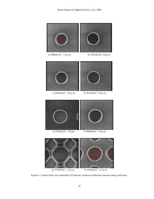
<strong>Ozean</strong> <strong>Journal</strong> <strong>of</strong> <strong>Applied</strong> <strong>Science</strong>s 1(1), 2008 a) 200mJ/cm 2 , -1.0 µ m b) 252mJ/cm2, -0.8 µ m c) 305mJ/cm 2 , -0.8 µ m d) 357mJ/cm 2 , -0.8 µ m e) 252mJ/cm 2 , -1.0 µm f) 305mJ/cm 2 , -1.0 µ m g) 357mJ/cm 2 , -1.0 µ m h) 410mJ/cm 2 , -0.2 µ m Figure 6. Contact holes size (nominally 0.8 micron) variation at different exposure energy and focus. 52
<strong>Ozean</strong> <strong>Journal</strong> <strong>of</strong> <strong>Applied</strong> <strong>Science</strong>s 1(1), 2008 (a) (b) Figure 7. Cross-section <strong>of</strong> contact holes after dry etching process: (a) magnification 10kX, (b) magnification 20 kX. The value <strong>of</strong> exposure energy and focus range affected the size and shape <strong>of</strong> patterns and therefore their quality. Increasing the energy enlarged the hole size and reduced the sidewall slope. However, reducing the energy caused under-exposure, and reduced the hole size. The photoresist also tended to remain at the bottom <strong>of</strong> the holes. Since the lens system <strong>of</strong> the stepper is based on convex lenses. As such, a positive focus range will cause the lenses to move closer to the wafer, therefore, causing larger feature size <strong>of</strong> the patterns. Surface topology can also cause problem for the contact holes photolithography process. Since this step is the last one <strong>of</strong> the front end process, there are many layers and patterns underneath resulting in very uneven surface. These surfaces will cause undesirable reflection during photolithography process, and, as a result, feature size cannot be well controlled. The process <strong>of</strong> planarization is introduced to reduce such a problem, although, it cannot be totally eliminated. CONCLUSION This research was performed to develop the most suitable process parameters for the photolithography <strong>of</strong> contact hole patterning process. These conditions were found to be 305 mJ/cm 2 <strong>of</strong> exposure energy and -1.0 micron <strong>of</strong> focus range. They were incorporated in TMEC’s 0.8 micron CMOS fabrication process technology to be used for IC and sensor fabrications. REFERENCES Hong, X. (2001). CVD and Dielectric Thin Film. In S.Helba, Introduction to semiconductor manufacturing Technology (pp. 390-413). New Jersey: Prentice Hall. James, R., Sheets, Bruce, & W., Smith (1998). Multilayer Resist Technology. In Bruce W. Smith, Microlithography <strong>Science</strong> and Technology (pp. 575-577). New York: Marcel Dekker. Nasby, R.D., Sniegowski, J. J., Smith, J. H., Montague, S., Barron, C. C., Eaton, W. P., McWhorter, P. J. Hetherington, D. L., Apblett C. A. & Fleming, J. G. (1996). Application <strong>of</strong> chemicalmechanical polishing to planarization Of surface-micromachined devices. Technical Digest <strong>of</strong> the Solid State Sensor and Actuator Workshop, 48-53. Zheng, Y., Dutta, M., Kotecki, C., & Zincke, C. (2002). Planarization for the Integration <strong>of</strong> CMOS and micro mirror arrays. Proc. <strong>of</strong> SPIE: Metrology,Inspection and process control for microlithography XVI, 4689, 1070-1076. 53