sn74lv245at octal bus transceiver with 3state outputs - CNC4PC
sn74lv245at octal bus transceiver with 3state outputs - CNC4PC
sn74lv245at octal bus transceiver with 3state outputs - CNC4PC

You also want an ePaper? Increase the reach of your titles
YUMPU automatically turns print PDFs into web optimized ePapers that Google loves.
Inputs Are TTL-Voltage Compatible<br />
4.5-V to 5.5-V V CC Operation<br />
Typical t pd of 3.5 ns at 5 V<br />
Typical V OLP (Output Ground Bounce)<br />
2.3 V at V CC = 5 V, T A = 25°C<br />
Supports Mixed-Mode Voltage Operation on<br />
All Ports<br />
<br />
<br />
<br />
<br />
SCLS605A − DECEMBER 2004 − MARCH 2005<br />
I off Supports Partial-Power-Down Mode<br />
Operation<br />
Latch-Up Performance Exceeds 250 mA Per<br />
JESD 17<br />
ESD Protection Exceeds JESD 22<br />
− 2000-V Human-Body Model (A114-A)<br />
− 1000-V Charged-Device Model (C101)<br />
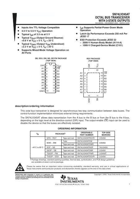
DB, DGV, DW, NS, OR PW PACKAGE<br />
(TOP VIEW)<br />
RGY PACKAGE<br />
(TOP VIEW)<br />
DIR<br />
A1<br />
A2<br />
A3<br />
A4<br />
A5<br />
A6<br />
A7<br />
A8<br />
GND<br />
1<br />
2<br />
3<br />
4<br />
5<br />
6<br />
7<br />
8<br />
9<br />
10<br />
20<br />
19<br />
18<br />
17<br />
16<br />
15<br />
14<br />
13<br />
12<br />
11<br />
V CC<br />
OE<br />
B1<br />
B2<br />
B3<br />
B4<br />
B5<br />
B6<br />
B7<br />
B8<br />
A1<br />
A2<br />
A3<br />
A4<br />
A5<br />
A6<br />
A7<br />
A8<br />
2<br />
3<br />
4<br />
5<br />
6<br />
7<br />
8<br />
9<br />
DIR<br />
B8 V<br />
1 20<br />
10 11<br />
GND<br />
CC<br />
19<br />
18<br />
17<br />
16<br />
15<br />
14<br />
13<br />
12<br />
OE<br />
B1<br />
B2<br />
B3<br />
B4<br />
B5<br />
B6<br />
B7<br />
description/ordering information<br />
This <strong>octal</strong> <strong>bus</strong> <strong>transceiver</strong> is designed for asynchronous two-way communication between data <strong>bus</strong>es. The<br />
control-function implementation minimizes external timing requirements.<br />
The SN74LV245AT allows data transmission from the A <strong>bus</strong> to the B <strong>bus</strong> or from the B <strong>bus</strong> to the A <strong>bus</strong>,<br />
depending on the logic level at the direction-control (DIR) input. The output-enable (OE) input can be used to<br />
disable the device so that the <strong>bus</strong>es are effectively isolated.<br />
TA<br />
ORDERING INFORMATION<br />
PACKAGE†<br />
ORDERABLE<br />
PART NUMBER<br />
QFN − RGY Tape and reel SN74LV245ATRGYR LV245A<br />
SOIC − DW<br />
Tube<br />
Tape and reel<br />
SN74LV245ATDW<br />
SN74LV245ATDWR<br />
TOP-SIDE<br />
MARKING<br />
LV245A<br />
−40°C to 85°C SOP − NS Tape and reel SN74LV245ATNSR 74LV245A<br />
SSOP − DB Tape and reel SN74LV245ATDBR LV245A<br />
TSSOP − PW Tape and reel SN74LV245ATPWR LV245AT<br />
TVSOP − DGV Tape and reel SN74LV245ATDGVR LV245A<br />
† Package drawings, standard packing quantities, thermal data, symbolization, and PCB design guidelines<br />
are available at www.ti.com/sc/package.<br />
Please be aware that an important notice concerning availability, standard warranty, and use in critical applications of<br />
Texas Instruments semiconductor products and disclaimers thereto appears at the end of this data sheet.<br />
<br />
<br />
<br />
<br />
Copyright © 2005, Texas Instruments Incorporated<br />
POST OFFICE BOX 655303 • DALLAS, TEXAS 75265<br />
1
SCLS605A − DECEMBER 2004 − MARCH 2005<br />
description/ordering information (continued)<br />
To ensure the high-impedance state during power up or power down, OE should be tied to V CC through a pullup<br />
resistor; the minimum value of the resistor is determined by the current-sinking capability of the driver.<br />
This device is fully specified for partial-power-down applications using I off . The I off circuitry disables the <strong>outputs</strong>,<br />
preventing damaging current backflow through the device when it is powered down.<br />
OE<br />
FUNCTION TABLE<br />
(each <strong>transceiver</strong>)<br />
INPUTS<br />
DIR<br />
OPERATION<br />
L L B data to A <strong>bus</strong><br />
L H A data to B <strong>bus</strong><br />
H X Isolation<br />
logic diagram (positive logic)<br />
DIR<br />
1<br />
19<br />
OE<br />
A1<br />
2<br />
18<br />
B1<br />
To Seven Other Channels<br />
2 POST OFFICE BOX 655303 • DALLAS, TEXAS 75265
SCLS605A − DECEMBER 2004 − MARCH 2005<br />
absolute maximum ratings over operating free-air temperature range (unless otherwise noted) †<br />
Supply voltage range, V CC . . . . . . . . . . . . . . . . . . . . . . . . . . . . . . . . . . . . . . . . . . . . . . . . . . . . . . . . . . −0.5 V to 7 V<br />
Input voltage range, V I (see Note 1) . . . . . . . . . . . . . . . . . . . . . . . . . . . . . . . . . . . . . . . . . . . . . . . . . . −0.5 V to 7 V<br />
Voltage range applied to any output in the high-impedance<br />
or power-off state, V O (see Note 1) . . . . . . . . . . . . . . . . . . . . . . . . . . . . . . . . . . . . . . . . . . . . . . . . −0.5 V to 7 V<br />
Output voltage range applied in the high or low state, V O (see Notes 1 and 2) . . . . . . −0.5 V to V CC + 0.5 V<br />
Input clamp current, I IK (V I < 0) . . . . . . . . . . . . . . . . . . . . . . . . . . . . . . . . . . . . . . . . . . . . . . . . . . . . . . . . . . . −20 mA<br />
Output clamp current, I OK (V O < 0 or V O > V CC ) . . . . . . . . . . . . . . . . . . . . . . . . . . . . . . . . . . . . . . . . . . . . ±50 mA<br />
Continuous output current, I O (V O = 0 to V CC ) . . . . . . . . . . . . . . . . . . . . . . . . . . . . . . . . . . . . . . . . . . . . . . ±35 mA<br />
Continuous current through V CC or GND . . . . . . . . . . . . . . . . . . . . . . . . . . . . . . . . . . . . . . . . . . . . . . . . . . . ±70 mA<br />
Package thermal impedance, θ JA (see Note 3): DB package . . . . . . . . . . . . . . . . . . . . . . . . . . . . . . . . . 70°C/W<br />
(see Note 3): DGV package . . . . . . . . . . . . . . . . . . . . . . . . . . . . . . . . 92°C/W<br />
(see Note 3): DW package . . . . . . . . . . . . . . . . . . . . . . . . . . . . . . . . . 58°C/W<br />
(see Note 3): NS package . . . . . . . . . . . . . . . . . . . . . . . . . . . . . . . . . 60°C/W<br />
(see Note 3): PW package . . . . . . . . . . . . . . . . . . . . . . . . . . . . . . . . . 83°C/W<br />
(see Note 4): RGY package . . . . . . . . . . . . . . . . . . . . . . . . . . . . . . . . 37°C/W<br />
Storage temperature range, T stg . . . . . . . . . . . . . . . . . . . . . . . . . . . . . . . . . . . . . . . . . . . . . . . . . . . −65°C to 150°C<br />
† Stresses beyond those listed under “absolute maximum ratings” may cause permanent damage to the device. These are stress ratings only, and<br />
functional operation of the device at these or any other conditions beyond those indicated under “recommended operating conditions” is not<br />
implied. Exposure to absolute-maximum-rated conditions for extended periods may affect device reliability.<br />
NOTES: 1. The input and output voltage ratings may be exceeded if the input and output current ratings are observed.<br />
2. This value is limited to 5.5 V maximum.<br />
3. The package thermal impedance is calculated in accordance <strong>with</strong> JESD 51-7.<br />
4. The package thermal impedance is calculated in accordance <strong>with</strong> JESD 51-5.<br />
recommended operating conditions (see Note 5)<br />
MIN MAX UNIT<br />
VCC Supply voltage 4.5 5.5 V<br />
VIH High-level input voltage VCC = 4.5 V to 5.5 V 2 V<br />
VIL Low-level input voltage VCC = 4.5 V to 5.5 V 0.8 V<br />
VI Input voltage 0 5.5 V<br />
VO<br />
Output voltage<br />
High or low state 0 VCC<br />
3-state 0 5.5<br />
IOH High-level output current VCC = 4.5 V to 5.5 V −16 mA<br />
IOL Low-level output current VCC = 4.5 V to 5.5 V 16 mA<br />
∆t/∆v Input transition rise or fall rate VCC = 4.5 V to 5.5 V 20 ns/V<br />
TA Operating free-air temperature −40 85 °C<br />
NOTE 5:<br />
All unused inputs of the device must be held at VCC or GND to ensure proper device operation. Refer to the TI application report,<br />
Implications of Slow or Floating CMOS Inputs, literature number SCBA004.<br />
V<br />
POST OFFICE BOX 655303 • DALLAS, TEXAS 75265<br />
3
SCLS605A − DECEMBER 2004 − MARCH 2005<br />
electrical characteristics over recommended operating free-air temperature range (unless<br />
otherwise noted)<br />
PARAMETER TEST CONDITIONS VCC<br />
VOH<br />
VOL<br />
TA = 25°C<br />
TA = −40°C<br />
TO 85°C<br />
MIN TYP MAX MIN MAX<br />
IOH = −50 µA 4.5 V 4.4 4.5 4.4<br />
IOH = −16 mA 4.5 V 3.8 3.8<br />
IOL = 50 µA 4.5 V 0 0.1 0.1<br />
IOL = 16 mA 4.5 V 0.55 0.55<br />
II VI = 5.5 V or GND 0 to 5.5 V ±0.1 ±1 µA<br />
IOZ VO = VCC or GND 5.5 V ±0.25 ±2.5 µA<br />
ICC VI = VCC or GND, IO = 0 5.5 V 2 20 µA<br />
∆ICC † One input at 3.4 V, Other inputs at VCC or GND 5.5 V 1.35 1.5 mA<br />
Ioff VI or VO = 0 to 5.5 V 0 0.5 5 µA<br />
Ci Control inputs VI = VCC or GND 5 V 3 pF<br />
Cio A or B port VO = VCC or GND 5 V 7 pF<br />
† This is the increase in supply current for each input at one of the specified TTL voltage levels rather than 0 V or VCC.<br />
switching characteristics over recommended operating free-air temperature range,<br />
V CC = 5 V ± 0.5 V (unless otherwise noted) (see Figure 1)<br />
PARAMETER<br />
tPLH<br />
tPHL<br />
tPZH<br />
tPZL<br />
tPHZ<br />
tPLZ<br />
FROM<br />
TO<br />
LOAD<br />
TA = 25°C<br />
(INPUT)<br />
(OUTPUT) CAPACITANCE MIN TYP MAX<br />
A or B B or A CL = 15 pF<br />
OE A or B CL = 15 pF<br />
OE A or B CL = 15 pF<br />
UNIT<br />
V<br />
V<br />
MIN MAX UNIT<br />
3.1 4.9 7.7 1 8.5<br />
2.3 4.9 7.7 1 8.5<br />
3.5 9.4 13.8 1 15<br />
3.7 9.4 13.8 1 15<br />
3.5 3.9 7.5 1 8<br />
2.6 3.9 7.5 1 8<br />
tPLH<br />
4.6 5.4 8.7 1 9.5<br />
A or B B or A CL = 50 pF<br />
tPHL<br />
4.7 5.4 8.7 1 9.5<br />
ns<br />
tPZH<br />
4.9 9.9 14.8 1 16<br />
OE A or B CL = 50 pF<br />
tPZL<br />
5.3 9.9 14.8 1 16<br />
ns<br />
tPHZ<br />
4.5 10.1 15.4 1 16.5<br />
OE A or B CL = 50 pF<br />
tPLZ<br />
4.1 10.1 15.4 1 16.5<br />
ns<br />
tsk(o) CL = 50 pF 1 1 ns<br />
ns<br />
ns<br />
ns<br />
noise characteristics, V CC = 5 V, C L = 50 pF (see Note 6)<br />
PARAMETER<br />
TA = 25°C<br />
MIN TYP MAX<br />
UNIT<br />
VOL(P) Quiet output, maximum dynamic VOL 1.1 1.5 V<br />
VOL(V) Quiet output, minimum dynamic VOL −1.1 −1.5 V<br />
VOH(V) Quiet output, minimum dynamic VOH 4 V<br />
VIH(D) High-level dynamic input voltage 2 V<br />
VIL(D) Low-level dynamic input voltage 0.8 V<br />
NOTE 6: Characteristics are for surface-mount packages only.<br />
4 POST OFFICE BOX 655303 • DALLAS, TEXAS 75265
SCLS605A − DECEMBER 2004 − MARCH 2005<br />
operating characteristics, V CC = 5 V, T A = 25°C<br />
PARAMETER TEST CONDITIONS TYP UNIT<br />
Cpd Power dissipation capacitance Outputs enabled CL = 50 pF, f = 10 MHz 19 pF<br />
POST OFFICE BOX 655303 • DALLAS, TEXAS 75265<br />
5
SCLS605A − DECEMBER 2004 − MARCH 2005<br />
PARAMETER MEASUREMENT INFORMATION<br />
From Output<br />
Under Test<br />
CL<br />
(see Note A)<br />
Test<br />
Point<br />
From Output<br />
Under Test<br />
CL<br />
(see Note A)<br />
RL = 1 kΩ<br />
S1<br />
VCC<br />
Open<br />
GND<br />
TEST<br />
tPLH/tPHL<br />
tPLZ/tPZL<br />
tPHZ/tPZH<br />
Open Drain<br />
S1<br />
Open<br />
VCC<br />
GND<br />
VCC<br />
LOAD CIRCUIT FOR<br />
TOTEM-POLE OUTPUTS<br />
LOAD CIRCUIT FOR<br />
3-STATE AND OPEN-DRAIN OUTPUTS<br />
Input<br />
tw<br />
1.5 V 1.5 V<br />
3 V<br />
0 V<br />
Timing Input<br />
Data Input<br />
tsu<br />
1.5 V<br />
th<br />
1.5 V 1.5 V<br />
3 V<br />
0 V<br />
3 V<br />
0 V<br />
VOLTAGE WAVEFORMS<br />
PULSE DURATION<br />
VOLTAGE WAVEFORMS<br />
SETUP AND HOLD TIMES<br />
Input<br />
1.5 V 1.5 V<br />
3 V<br />
0 V<br />
Output<br />
Control<br />
1.5 V 1.5 V<br />
3 V<br />
0 V<br />
In-Phase<br />
Output<br />
Out-of-Phase<br />
Output<br />
tPLH<br />
tPHL<br />
50% VCC<br />
50% VCC<br />
tPHL<br />
VOH<br />
50% VCC<br />
VOL<br />
tPLH<br />
VOH<br />
50% VCC<br />
VOL<br />
VOLTAGE WAVEFORMS<br />
PROPAGATION DELAY TIMES<br />
INVERTING AND NONINVERTING OUTPUTS<br />
Output<br />
Waveform 1<br />
S1 at VCC<br />
(see Note B)<br />
Output<br />
Waveform 2<br />
S1 at GND<br />
(see Note B)<br />
tPZL<br />
tPZH<br />
50% VCC<br />
50% VCC<br />
tPLZ<br />
VOL + 0.3 V<br />
VOL<br />
tPHZ<br />
VOLTAGE WAVEFORMS<br />
ENABLE AND DISABLE TIMES<br />
LOW- AND HIGH-LEVEL ENABLING<br />
≈VCC<br />
VOH<br />
VOH − 0.3 V<br />
≈0 V<br />
NOTES: A. CL includes probe and jig capacitance.<br />
B. Waveform 1 is for an output <strong>with</strong> internal conditions such that the output is low, except when disabled by the output control.<br />
Waveform 2 is for an output <strong>with</strong> internal conditions such that the output is high, except when disabled by the output control.<br />
C. All input pulses are supplied by generators having the following characteristics: PRR ≤ 1 MHz, ZO = 50 Ω, tr ≤ 3 ns, tf ≤ 3 ns.<br />
D. The <strong>outputs</strong> are measured one at a time, <strong>with</strong> one input transition per measurement.<br />
E. tPLZ and tPHZ are the same as tdis.<br />
F. tPZL and tPZH are the same as ten.<br />
G. tPHL and tPLH are the same as tpd.<br />
H. All parameters and waveforms are not applicable to all devices.<br />
Figure 1. Load Circuit and Voltage Waveforms<br />
6 POST OFFICE BOX 655303 • DALLAS, TEXAS 75265