0-1 NOVA-LUKE Motherboard 1
0-1 NOVA-LUKE Motherboard 1
0-1 NOVA-LUKE Motherboard 1
You also want an ePaper? Increase the reach of your titles
YUMPU automatically turns print PDFs into web optimized ePapers that Google loves.
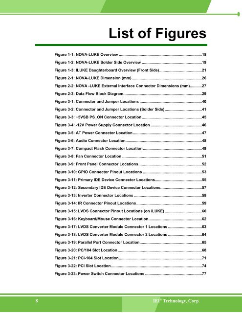
List of Figures<br />
Figure 1-1: <strong>NOVA</strong>-<strong>LUKE</strong> Overview ............................................................................18<br />
Figure 1-2: <strong>NOVA</strong>-<strong>LUKE</strong> Solder Side Overview .......................................................19<br />
Figure 1-3: I<strong>LUKE</strong> Daughterboard Overview (Front Side).......................................21<br />
Figure 2-1: <strong>NOVA</strong>-<strong>LUKE</strong> Dimension (mm) ................................................................26<br />
Figure 2-2: <strong>NOVA</strong> -<strong>LUKE</strong> External Interface Connector Dimensions (mm)...........27<br />
Figure 2-3: Data Flow Block Diagram........................................................................29<br />
Figure 3-1: Connector and Jumper Locations .........................................................40<br />
Figure 3-2: Connector and Jumper Locations (Solder Side)..................................41<br />
Figure 3-3: +5VSB PS_ON Connector Location.......................................................45<br />
Figure 3-4: -12V Power Supply Connector Location ...............................................46<br />
Figure 3-5: AT Power Connector Location ...............................................................47<br />
Figure 3-6: Audio Connector Location......................................................................48<br />
Figure 3-7: Compact Flash Connector Location......................................................49<br />
Figure 3-8: Fan Connector Location .........................................................................51<br />
Figure 3-9: Front Panel Connector Locations..........................................................52<br />
Figure 3-10: GPIO Connector Pinout Locations ......................................................53<br />
Figure 3-11: Primary IDE Device Connector Locations...........................................55<br />
Figure 3-12: Secondary IDE Device Connector Locations......................................57<br />
Figure 3-13: Inverter Connector Locations ..............................................................58<br />
Figure 3-14: IR Connector Pinout Locations............................................................59<br />
Figure 3-15: LVDS Connector Pinout Locations (on i<strong>LUKE</strong>) ..................................60<br />
Figure 3-16: Keyboard/Mouse Connector Location.................................................62<br />
Figure 3-17: LVDS Converter Module Connector 1 Locations ...............................63<br />
Figure 3-18: LVDS Converter Module Connector 2 Locations ...............................64<br />
Figure 3-19: Parallel Port Connector Location.........................................................65<br />
Figure 3-20: PC/104 Slot Location .............................................................................68<br />
Figure 3-21: PCI-104 Slot Location............................................................................71<br />
Figure 3-22: PCI Slot Location ...................................................................................74<br />
Figure 3-23: Power Switch Connector Locations ....................................................77<br />
8 IEI ® Technology, Corp.<br />
0-8


