Microcomputer Circuits and Processes
Microcomputer Circuits and Processes
Microcomputer Circuits and Processes

Create successful ePaper yourself
Turn your PDF publications into a flip-book with our unique Google optimized e-Paper software.
General editor.<br />
Revised Nuffield<br />
Advanced Physics<br />
John Harris<br />
Consultant editor<br />
E. J. Wenham<br />
Author of this book<br />
Colin Price
PHYSICS<br />
MICROCOMPUTER<br />
CIRCUITS AND<br />
PROCESSES<br />
REVISED NUFFIElD ADVANCED SCIENCE<br />
Pu1:'11c;:hpnfnr thp Nllffipln-rhplc;:p~ Curriculum Trust<br />
by 1<br />
Im~~~I~llilil<br />
N12435
Longman Group Limited<br />
Longman House, Burnt Mill, Harlow, Essex CM20 2JE, Engl<strong>and</strong><br />
<strong>and</strong> Associated Companies throughout the World<br />
Copyright © 1985 The Nuffield-Chelsea Curriculum Trust<br />
Design <strong>and</strong> art direction by Ivan Dodd<br />
Illustrations by Oxford Illustrators Limited<br />
Filmset in Times Roman <strong>and</strong> Univers <strong>and</strong> made <strong>and</strong> printed in Great<br />
Britain at The Bath Press, Avon<br />
ISBN 0 582 35423 4<br />
All rights reserved. No part of this publication may be reproduced,<br />
stored in a retrieval system, or transmitted in any form or by any<br />
means - electronic, mechanical, photocopying, or otherwise - without<br />
the prior written permission of the Publishers.<br />
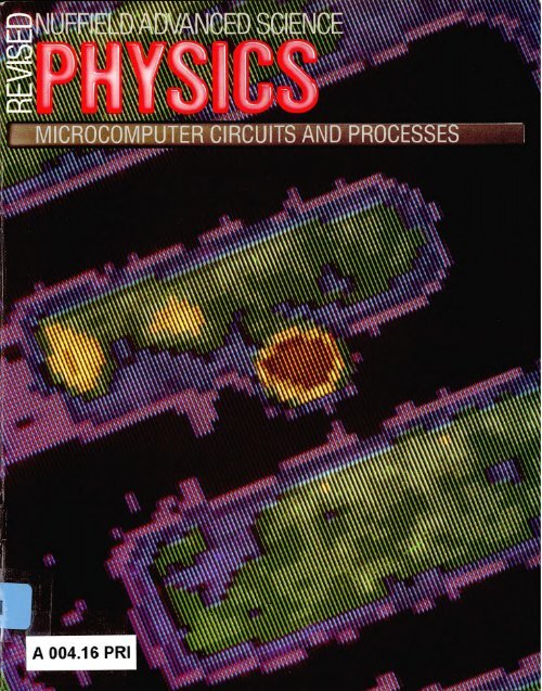
Cover<br />
The photograph on the back cover shows individual gates of a microchip made visible by EBIC (electron beam induced current)<br />
inside a scanning electron microscope. A defective gate (no glow) shows up amongst operating cells (fluorescent glow).<br />
The photograph on the front cover shows the defective cell of the microchip analysed by an elemental analyser built into the<br />
electron microscope. The material distribution at the defective emitter of the cell is mapped by computer on a colour monitor screen<br />
in colours representing relative material thickness.<br />
The width between adjoining tracks in each case is 10 !-Lm.<br />
Courtesy ERA Technology + Micro Consultants/Link Systems<br />
Photographs: Paul Brierley
CONTENTS<br />
PROLOGUE<br />
page iv<br />
Chapter 1 A HISTORY OF THE MICROPROCESSOR 1<br />
Chapter 2 THE ELECTRONICS OF A MICROCOMPUTER 8<br />
Chapter 3 RUNNING A SIMPLE PROGRAM 26<br />
Chapter 4 MEMORIES, INTERFACES, AND APPLICATIONS 44<br />
EPILOGUE 75<br />
BIBLIOGRAPHY 75<br />
INDEX 76<br />
.1.
PROLOGUE<br />
This Reader explains how microcomputers work. It does not refer to<br />
anyone computer, but all ideas discussed are relevant to any computer.<br />
It begins with ...<br />
CHAPTER 1 where the history of the microprocessor is traced out from ancient to<br />
modern times. It continues with ...<br />
CHAPTER 2 which looks at the electronics of a microcomputer, building up a simple<br />
machine from scratch.<br />
CHAPTER 3 describes how a small program stored in memory actually gets all the<br />
electronics working, to carry out the programmer's desires.<br />
CHAPTER 4 is about how microcomputers can be used to make measurements <strong>and</strong><br />
display results of computations. There are also some notes on computer<br />
memory.<br />
Although no reference is made to any commercial microcomputer, all<br />
the circuits drawn in this Reader were tested by building a small<br />
computer. Any differences between the text <strong>and</strong> reality are small, <strong>and</strong><br />
intended to make everything a little clearer for you. If you know<br />
nothing about these things, I hope you learn something. If you are<br />
already a microprocessor boffin, there will still be some pieces of<br />
interest.<br />
I must thank the Intel Corporation of Santa Clara, California, for<br />
supplying photographs <strong>and</strong> numerous other data for use in this Reader.<br />
And they make good microprocessors too. Thanks to David Chantrey<br />
for help in correcting the original text, any remaining mistake is my<br />
own.<br />
Colin Price<br />
iv
CHAPTER 1<br />
A HISTORY OF THE<br />
MICROPROCESSOR<br />
SOWING<br />
THE SEEDS<br />
The revolution now shaking every aspect of life from banking <strong>and</strong><br />
medicine to education <strong>and</strong> home life began in 1947 in the Bell<br />
Laboratories with the invention of the transistor by Brattain, Bardeen,<br />
<strong>and</strong> Shockley. This small amplifier (which now in modern memory<br />
circuits can be made very small- 6 Ilm x 6 Ilm) quickly replaced the<br />
large power-consuming vacuum tube. The evolution of the microprocessor<br />
from the humble transistor illustrates the relationship between<br />
technology <strong>and</strong> economics, <strong>and</strong> also how the technology of electronic<br />
device production is related to the desired applications of electronics at<br />
any time.<br />
For example, it is difficult to build a practical computer which needs<br />
a large number of switching circuits using vacuum tubes. But when the<br />
transistor was invented, the situation at once changed. In the 1950s the<br />
transistor did replace vacuum tubes in many applications, but as far as<br />
building computers was concerned, there still remained the problem of<br />
the myriad of connections which had to be made between individual<br />
transistors. That meant time <strong>and</strong> materials. Also, studies made in the<br />
early 1950s suggested that only 20 computers would be needed to<br />
satisfy the World's needs. The market did not exist, <strong>and</strong> technology was<br />
then unable to stimulate it. The solution to the interconnection problem<br />
was the integrated circuit, invented by Jack Kilby of Texas Instruments<br />
in 1958, <strong>and</strong> Bob Noyce, at Fairchild in 1959.<br />
THE INTEGRATED CIRCUIT INDUSTRY<br />
Manufacturing an integrated circuit (IC) involves the 'printing' of many<br />
transistors, with a sprinkling of resistors <strong>and</strong> capacitors, on to a wafer of<br />
silicon. Those in the trade call this printing process photolithography<br />
<strong>and</strong> solid-state diffusion. Using this technology, hundreds of very small,<br />
identical circuits can be made simultaneously on one wafer of silicon.<br />
These circuits are bound to be cheap. But most important is the ability<br />
to print the interconnections between the individual transitors on to the<br />
silicon chip, removing the need for manually wiring the circuit together.<br />
So costs were"again reduced. As reliability of the circuits improved<br />
dramatically, so maintenance costs fell too.<br />
Such economic trends inspired manufacturers to research into<br />
further miniaturization, <strong>and</strong> in 1965, Gordon Moore, later chairman of<br />
Intel Corporation, predicted that during the next decade the number of<br />
transistors per integrated circuit would double every year. This exponential<br />
'law' held good, <strong>and</strong> remained good into the 1980s.The graph<br />
in figure 1.1shows this law, from the first IC of 1959containing just one<br />
1
transistor, through the logic circuits of 1965 <strong>and</strong> the 4096-transistor<br />
memory of 1971, to the 4 million-bit 'bubble' memory introduced in<br />
1982. Of course the rate of doubling has slowed recently, but there is<br />
still anticipation of further miniaturization.<br />
~ 4194 304<br />
:::I<br />
e<br />
'y 1048576<br />
•l:L<br />
e 262144<br />
0<br />
1;;<br />
.;; 65536<br />
c<br />
..<br />
t!<br />
16384<br />
'0<br />
j 4096<br />
E :::I<br />
Z 1024<br />
, ,,<br />
256<br />
64<br />
16<br />
4<br />
63 65 67 69 71 73 75 77 79 81<br />
Year<br />
Figure 1.1<br />
Graph showing 'Moore's Law' - the doubling of number of transistors per Ie per year.<br />
The 4-megabit bubble memory introduced in 1982 does not use transistor technology.<br />
As any industry grows <strong>and</strong> gains experience its production costs fall,<br />
but the IC industry has been unique in achieving a constant doubling in<br />
component density coupled with falling costs. How has this been<br />
achieved? It is due to the IC concept, replacing transistor-based circuits<br />
in traditional equipment, producing smaller, more reliable, easily<br />
assembled devices. Much of the success of the IC industry has come<br />
from stimulating new markets. A good example is computer memory.<br />
Up to the end of the 1960s, computer memory was made from small<br />
rings of magnetic material sewn together by electrical wires. It worked,<br />
but compared with the component densities being achieved in the IC,<br />
the package was bulky. People in the semiconductor industry realized<br />
this, <strong>and</strong> understood that the requirements of computer memory - a<br />
large number of storage cells connected with a small number of leads -<br />
could be met by specially designed IC chips. Companies were founded<br />
with the sole purpose of memory manufacture, <strong>and</strong> as miniaturization<br />
continued <strong>and</strong> prices fell, semiconductor memory became established as<br />
the st<strong>and</strong>ard. Thanks to these devices, the large, room-sized computers<br />
of the 1950s <strong>and</strong> 1960s, with their hundreds of kilometres of wiring,<br />
could be made smaller <strong>and</strong> more powerful. The mainframe <strong>and</strong><br />
minicomputers were born.<br />
2
BIRTH OF THE MICROPROCESSOR<br />
- A SOLUTION TO A PROBLEM<br />
The electronic systems manufacturers of the late 1960s were able to<br />
produce quite interesting products by engineering custom-designed<br />
ICs, each doing a specific job. Several tens or even hundreds of chips<br />
<strong>and</strong> other components were connected together by soldering them onto<br />
printed circuit boards. As the complexity of designs increased, this<br />
method of production became very expensive, <strong>and</strong> could only be<br />
employed when large production runs were involved, or else for<br />
government or military applications. A radically different approach to<br />
construction was needed.<br />
In 1969, Intel, one of today's leading producers of microprocessors,<br />
was commissioned to design some dedicated IC chips for a Japanese<br />
high-performance calculator. Their engineers decided that, using the<br />
traditional approach, they would need to design about 12 chips of<br />
around 4000 transistors per chip. That was pushing the current<br />
technology a bit (see figure 1.1) <strong>and</strong> would still leave a nasty interconnection<br />
problem. Intel's engineers were familiar with minicomputers<br />
<strong>and</strong> realized that a computer could be programmed to do all the clever<br />
functions needed for this calculator. Of course, a minicomputer was<br />
expensive <strong>and</strong> certainly not h<strong>and</strong>-held. But they also realized that they<br />
had, by then, sufficient technology to put some of the computer's<br />
functions onto a single chip <strong>and</strong> connect this to memory chips already<br />
on the market. The first microprocessor, the Intel 4004, was born.<br />
But how exactly did this solve the calculator design problem? It was<br />
all a question of how to approach a problem. Instead of the 12<br />
calculator chips, each performing a specific job, one microprocessor<br />
chip would be made which could carry out a few very simple tasks. The<br />
different complex functions needed for the calculator could be produced<br />
by the microprocessor being made to carry out its simple tasks in a<br />
repeating but Jrdered fashion. The instructions needed by the microprocessor<br />
to do this would be stored in memory chips, sent to the<br />
microprocessor, <strong>and</strong> implemented. Seemingly a long-winded procedure<br />
it could be made to work since ICs can be coaxed along at very high<br />
speeds, needing only microseconds to do a single task.<br />
The implications of this alternative approach were very profound.<br />
The same microprocessor as designed for the calculator could be used<br />
in endless other devices - watches, thermostats, cash registers. No new<br />
custom-designed ICs would be needed, the 'hardware' would remain<br />
intact; only the program put into memory, the 'software', would need to<br />
be changed to suit the new application. Manufacturers would have a<br />
high-volume product on their h<strong>and</strong>s, <strong>and</strong> soon would have smiles as<br />
wide as a television screen.<br />
Such innovation did not catch on overnight. Intel's 4004, which was<br />
heralded as the device that would make instruments <strong>and</strong> machines<br />
'intelligent', did not achieve that status. A great improvement came in<br />
1974with the 8080 microprocessor, designed by Masatoshi Shima (who<br />
later designed the Z80 for Zilog, the now famous hobby microprocessor).<br />
The 8080 had the ability to carry out an enormous range of<br />
3
tasks (large computing 'power'), was fast, <strong>and</strong> had the ability to control<br />
a wide range of other devices. The modern version of the 8080, the 8085<br />
(which you can buy for a few pounds) is firmly established as one of the<br />
st<strong>and</strong>ard 8-bit processors of the decade. No bigger than a baby's<br />
fingernail, it comes packaged in a few grams of plastic with 40 terminals<br />
tapping its enormous potential (figure 1.2).<br />
Figure 1.2<br />
The birth of the 8085 microprocessor chip.<br />
Intel Corporation (UK) Ltd<br />
RESPONSE TO THE FIRST MICROPROCESSOR<br />
In mechanics, momentum must be conserved; but in the electronics<br />
industry it seems to increase! It had taken only three years since the<br />
introduction of the 4004 for.the total number of microprocessors in use<br />
to exceed the combined numbers of all minicomputers <strong>and</strong> mainframes.<br />
In 1974there were 19processors on the market, <strong>and</strong> one year later there<br />
were 40. Different manufacturers aimed at different markets: RCA<br />
developed a CMOS (Complementary Metal Oxide Semiconductor)<br />
processor, using practically no current; Texas Instruments developed a<br />
4-bit processor for games applications. Advances in design included<br />
putting the memory, input/output circuits, <strong>and</strong> even analogue-todigital<br />
converters on the processor chip, resulting in single-chip<br />
4
microcontrollers. Figure 1.3 outlines the development of the industry<br />
reminding us of the reducing size of the elements thereby increasing<br />
chip density.<br />
l) 10 6<br />
Xl<br />
2a.<br />
2<br />
u<br />
'E<br />
,5 r.!<br />
0<br />
ti<br />
'iii<br />
c<br />
~<br />
'0<br />
j<br />
E<br />
~<br />
z<br />
.- (I)<br />
" •..<br />
(I) c:<br />
(I)<br />
"iQc:<br />
uo<br />
C/l'-<br />
ee<br />
:lCl<br />
E'-<br />
Year<br />
of introduction<br />
Figure 1.3<br />
Evolution of the technology of making les is shown by the increasingly large transistor<br />
densities being obtained.<br />
By the 1970s between 1000 <strong>and</strong> 10000 transistors could be put on a<br />
single chip. This medium-scale integration (MSI) was used to make the<br />
4004, 8080, <strong>and</strong> 8085 processors. Large-scale integration (LSI), 10000 to<br />
100000 transistors on a chip, dominated the market in the late 1970s<br />
<strong>and</strong> early 1980s. It was used in the production of processors such as the<br />
16-bit 8086 <strong>and</strong> 8088 used by IBM in their personal computer launched<br />
in 1984. Large-scale integration will be followed by very large-scale<br />
integration (VLSi) as more than 100000 transistors are put on to a chip.<br />
The iAPX 432 contains 225000 transistors <strong>and</strong> is the product of 20<br />
million dollars <strong>and</strong> 100 worker-years of development. This processor,<br />
on a single chip, has all the power of a minicomputer which would fill a<br />
wardrobe-sized cabinet. It can execute 2 million instructions per<br />
second.<br />
APPLICATIONS - THE CREATION OF NEW MARKETS<br />
When the initial 4004 development was under way, marketing departments<br />
envisaged the microprocessor as being sold only as minicomputer<br />
replacements, <strong>and</strong> made sales estimates of only a few thous<strong>and</strong><br />
per year. In 1981 sales of the latest 16-bit processors rose above the<br />
5
800000 mark. Such high sales resulted from the creation of new<br />
markets as microprocessors appeared. The great boom in digital<br />
watches, pocket calculators, <strong>and</strong> electronic games of the late 1970s is a<br />
good example of such a market. In electronic instrumentation (oscilloscopes,<br />
chromatographs, <strong>and</strong> surveying instruments, for example)<br />
which had been a stable, mature market, the microprocessor brought<br />
along a rebirth; instruments not only would make measurements but<br />
analyse the data as well.<br />
It is now impossible to escape from the processor. This is perhaps<br />
most evident in the consumer area: games, inside television sets, hi~fi<br />
sets, <strong>and</strong> video recorders, <strong>and</strong> of course personal computers all depend<br />
on them. In medicine the microprocessor directs life-saving <strong>and</strong> lifesupport<br />
equipment, <strong>and</strong> has enabled the modern science of genetic<br />
engineering to develop. In commerce, word processing, telephone<br />
exchanges, <strong>and</strong> banking systems rely on the microprocessor; indeed,<br />
future developments lie in this area. Complete office units will be<br />
microprocessor based, where dictation, passing interdepartmental<br />
memos, <strong>and</strong> so on, will all be managed by microcomputers. The<br />
cashless society, where the familiar 'cash..;card' will contain a memory<br />
chip containing details of your accounts, is almost upon us. Supermarkets<br />
will no longer have tills but will automatically debit you via<br />
such a card.<br />
Towards the more academic pursuits, Artifical Intelligence is being<br />
seriously researched. Microprocessor-controlled voice-synthesis chips<br />
are on the hobby market <strong>and</strong> voice recognition <strong>and</strong> visual shape<br />
recognition are being investigated.<br />
TODAY'S PROBLEMS ARE TOMORROW'S DEVELOPMENTS<br />
Little has been said so far of the software side of the microprocessor<br />
industry. Remember that when the microprocessor was born, so also<br />
was the need to program it, to make it work. The history of the chip, as<br />
described above, is one of increasing complexity <strong>and</strong> power while<br />
reducing cost. But as the processor became more powerful, so the<br />
complexity of the programs increased. Software became very expensive,<br />
as you will know if you have ever bought games for your own computer.<br />
Different manufacturers have different strategies, but there are two very<br />
obvious ones at the time of writing. Firstly, when a manufacturer has<br />
just marketed a microprocessor, he knows that the programmers will be<br />
busily writing operating systems, compilers, business packages, <strong>and</strong> the<br />
like; <strong>and</strong> the research <strong>and</strong> development departments will already be<br />
busy on the next generation of hardware. Now all of this activity must<br />
be co-ordinated so that programs written on today's machine will be<br />
more-or-Iess compatible with tomorrow's machine, so they can run<br />
with the minimum of change. Such a philosophy will be welcomed by<br />
the buyer of a particular microprocessor system who does not want to<br />
throw out his computer every five years. Of all the manufacturers of<br />
microprocessors around, those who are most successful are the ones<br />
that pursue a policy of open-planned development.<br />
6
The second strategy chosen by some manufacturers is a subtle move<br />
away from software by replacing some programs by special chips<br />
designed to carry out certain functions. In the light of what has been<br />
said, you may think this sounds like going into reverse gear, but I did<br />
say it was a subtle move. A good example is the 8087 Numeric Data<br />
Processor, marketed by Intel. This chip, a microprocessor in its own<br />
right, sits inside a system quite close to the central microprocessor,<br />
which could be an 8086. The 8087 hangs around until a mathematical<br />
job is to be done, anything from adding to computing a trigonometric<br />
function. Then it springs into action, doing the mathematics about 100<br />
times faster than a software program stored in memory.<br />
The microprocessor revolution has touched all of us, from the<br />
company executive who has everything programmable to the farmer in<br />
India who depends on satellite weather pictures. In about a decade, it<br />
has become possible for you to buy, for several pounds, a microprocessor<br />
chip as powerful as a room-sized machine; <strong>and</strong> all of this by<br />
return of post. I hope you will try it out one day.<br />
7
CHAPTER 2<br />
THE ELECTRONICS<br />
MICROCOMPUTER<br />
OF A<br />
If you spend a few thous<strong>and</strong> pounds on buying a minicomputer - a<br />
wardrobe-sized cabinet where the processing is done by several boards<br />
full of medium-scale integrated circuits - or if you spend a few hundred<br />
pounds or less on a microcomputer, where the processing is done by"an<br />
LSI microprocessor like the 8085, then your computer will always have<br />
three types of circuit:<br />
a central processing unit (CPU);<br />
some memory;<br />
input <strong>and</strong> output devices - keyboard, television screen, printer, etc.<br />
This chapter is about how these three types of circuit are connected<br />
together. We shall think about a small microcomputer, where the CPU<br />
is a microprocessor, just like the one in the laboratory or even in your<br />
home.<br />
GETTING IT TOGETHER - THE BUS CONCEPT<br />
The three circuit types must be connected together; figure 2.1 suggests<br />
two ways of doing this. The first suggestion involves wires between each<br />
device. This may work, but would be clumsy. In the second suggestion,<br />
each device is connected in parallel to a set of wires called a bus.<br />
The bus is drawn on circuit diagrams as a wide channel <strong>and</strong>, in<br />
reality, consists of many parallel wires carrying signals. Each device -<br />
CPU, memory, keyboard, television screen - is connected to or 'hangs<br />
on' the bus.<br />
(a)<br />
television<br />
screen<br />
D<br />
printer<br />
cPU<br />
Figure<br />
2.1(a)<br />
Interconnecting computer devices: wires connect each device.<br />
8
(b)<br />
D<br />
II<br />
CPU<br />
_____ ~----- w;'es althe bus<br />
Figure 2.1(b)<br />
Interconnecting computer devices: the efficient bus connection.<br />
It saves a lot of wires, but there isjust one problem. What happens if<br />
two devices put their signals onto the bus simultaneously? This is<br />
shown in figure 2.2, where just one wire of the bus is shown, <strong>and</strong> two<br />
logic inverters are shown connected. The output of one is high <strong>and</strong> the<br />
output of the second is low. What happens?<br />
The bus wire cannot<br />
be both low <strong>and</strong> high<br />
Figure 2.2<br />
There is a problem when two devices put different signal levels on to the bus. This<br />
situation must be avoided.<br />
Almost certainly, something will get very hot <strong>and</strong> be damaged; at<br />
the very least the system will not work. This is called bus contention, <strong>and</strong><br />
steps must be taken to ensure that no two devices put their signals on<br />
the bus together. In technical jargon, no two devices may 'talk' to the<br />
bus simultaneously. This is achieved using a type oflogic gate called the<br />
'Tri-State' gate (which is a trademark of National Semiconductor<br />
Corporation). A tristate gate does not have three different logic states,<br />
but is like a normal logic gate in se'rieswith a switch. Look at figure 2.3<br />
which shows a tristate inverter gate. The idea is that a control signal is<br />
able to connect the gate to its output. This is called 'enabling' the gate. If<br />
the enable is low, then there is no output from the gate, neither high nor<br />
low. The gate is in a 'high-impedance' state, meaning that anything<br />
connected to its output does not know it is there. When the gate is<br />
9
enabled, as the truth table in figure 2.3 shows, it behaves just like a<br />
normal inverter.<br />
normal<br />
inverter<br />
input __ -+----1 o------lf---e output<br />
enable<br />
input enable output<br />
0 0 Z<br />
1 0 Z<br />
0 1 1<br />
1 1 0<br />
Circuit symbol<br />
Z means 'high impedance',<br />
i.e., not connected<br />
Figure 2.3<br />
The Tn-State buffer. (Tri-State is a trademark of the National Semiconductor<br />
Corporation.)<br />
To solve our problem of bus contention, tristate buffers are used.<br />
You can think of these simply as switches, many ~fthem controlled by a<br />
common enable. Figure 2.4 shows the beginnings of the computer<br />
system, with the CPU, a printer, <strong>and</strong> a television screen connected to<br />
the bus. The printer <strong>and</strong> television screen hang on via tristate buffers.<br />
The CPU contains its own buffers <strong>and</strong> can hang on the bus when it<br />
wants to.<br />
D<br />
television<br />
screen<br />
printer<br />
CPU<br />
control<br />
control<br />
Figure 2.4<br />
Connecting to the bus via tristate buffers.<br />
10
Look again at figure 2.4. You will see that the buffers' enable<br />
terminals are connected to wires labelled 'control', which must ultimately<br />
be connected to the CPU. The CPU will decide when either<br />
device will be enabled on to the bus. As you continue reading this<br />
chapter, you will realize that the CPU has a lot of controlling to do, <strong>and</strong><br />
its control connections to the various devices on the bus are therefore<br />
sent down the control bus. You will meet the control signals on this bus<br />
one by one.<br />
The situation so far is shown in figure 2.5. We have not given a name<br />
to the top bus; think of it for the moment as an 'information' bus used to<br />
shunt numbers to <strong>and</strong> fro. So how many wires should be used in this<br />
bus, or put another way, how 'wide' should it be? Well, you know from<br />
binary arithmetic that to write the numbers 0 to 10 in binary, you need<br />
four binary digits or bits. For example 2 10 = 0010 2 <strong>and</strong> 9 10 is 1001 2 .* So<br />
if we only wanted to send numbers from 0 to 10 down the bus, 4 wires<br />
would do. So it was in the days of the 4-bit 4004. But if you want to send<br />
English characters <strong>and</strong> words down the bus then you need a wider bus.<br />
Taking 8 bits gives at once 2 8 = 256 possible symbols. That sounds a bit<br />
more like it, but there is a bit more to it than that, as we will now see<br />
when we look at computer memory.<br />
,...--------,<br />
information<br />
bus<br />
CPU<br />
control<br />
bus<br />
D<br />
television<br />
screen<br />
printer<br />
Figure 2.5<br />
Addition of control bus provides signals to enable the buffers.<br />
A FIRST LOOK AT MEMORY<br />
The basic requirement of memory is to be able to write some<br />
information into it, leave it there, <strong>and</strong> come back later to read it. This<br />
can be done with floppy disks, tape, or pencil <strong>and</strong> paper, but here we are<br />
concerned with the type of memory all computers have, semiconductor<br />
memory. The basic unit of memory is a single storage cell which may<br />
hold binary 0 or binary 1. We will not worry about what electronics<br />
could be in the cell just yet - you probably know one arrangement of<br />
gates or flip-flops that could do the job. It must be possible to read <strong>and</strong><br />
* 2 10 (read as 'two base ten') means 2 in our common base-IO counting system. 0010 2 (read<br />
as 'one zero base two') = (l X 2 1 ) + (0 x 2°) = 2 10 • And 1001 2 is (1 X 2 3 ) + (0 X 2 2 ) +<br />
(Ox2 1 )+(l X 2°)=9 10 •<br />
11
D<br />
memory<br />
cell<br />
storing<br />
binary 0<br />
storing<br />
binary 1<br />
Figure 2.6<br />
Cells of RAM (r<strong>and</strong>om access memory).<br />
R<br />
o<br />
W<br />
S<br />
E<br />
L<br />
E<br />
C<br />
T<br />
I COLUMN SELECT I<br />
Figure 2.7<br />
Structure of a 256-cell memory chip.<br />
.:<br />
f 3<br />
write from <strong>and</strong> to these cells, <strong>and</strong> to choose which cells you are<br />
interested in. These cells, one of which is shown in figure 2.6, form<br />
r<strong>and</strong>om access memory (RAM).<br />
To make up a useful memory chip, these cells are packed into a<br />
square array. We shall think about a 16 by 16 cell array (256 cells in<br />
total) for simplicity; a modern 2164 memory chip contains 4 groups of<br />
128 by 128 cells, giving 65536 cells in all! A rather smaller memory<br />
array is shown in figure 2.7.<br />
Controlling the memory cells are two blocks of logic circuits: a set of<br />
row selectors on the side <strong>and</strong> the column select at the bottom. These<br />
circuits pick out one particular cell from the 256 by specifying on which<br />
one of the 16 rows the cell lives <strong>and</strong> on which one of the 16 columns it<br />
lives. So, both row <strong>and</strong> column select have 16 outputs. Now 16 is 24, so<br />
only 4 bits of information are needed to address any of the 16 rows or<br />
columns. That is why each select block is driven by a 4-bit binary<br />
number, as shown in figure 2.8.<br />
Here, the row select is being driven by binary 0100 (4 10 ) <strong>and</strong> the<br />
column select is being driven by binary 0011 (3 10 ), so the cell being<br />
addressed is row 4, column 3. (When looking at the diagram, do not<br />
overlook the existence of row 0 <strong>and</strong> column 0.) In this way, each<br />
memory cell may be specified by two 4-bit binary numbers, <strong>and</strong> this is<br />
called the address of the memory cell, in this case 0100 001l.<br />
Now that we are able to address memory, we must look at how data<br />
is got in <strong>and</strong> out of the cells. One way of doing this on the memory chip<br />
is to put some in-out circuits next to the column selects, as in figure 2.9.<br />
This block has a data-in wire <strong>and</strong> a data-out wire. If data in = 1 <strong>and</strong> a<br />
write into memory is performed, then the 1 is stored in the cell defined<br />
by the two 4-bit address numbers. Similarly, if the contents of cell 0111<br />
1101 are needed, this address is sent to the select logic, <strong>and</strong> the contents<br />
of this cell are read out via data out.<br />
data in (0 or 1) data out (0 or 1)<br />
Figure 2.8<br />
Addressing one cell of a 256-cell<br />
memory chip.<br />
RD WR<br />
control lines<br />
address<br />
Figure 2.9<br />
Additional circuitry to get data in <strong>and</strong> out of 256-bit memory.<br />
12
RD<br />
WR<br />
in/<br />
out<br />
8·bit address<br />
row/column<br />
select<br />
256 cells<br />
memory<br />
data in/out<br />
(one bit)<br />
iigure 2.10<br />
~epresentation of 256-bit memory as it<br />
lay appear in a manufacturer's<br />
>atabook. Note address lines, data line,<br />
nd read (RD) <strong>and</strong> write (WR) lines.<br />
To perform reads <strong>and</strong> writes, the in-out circuits must receive some<br />
control signals, defining READ or WRITE. These come from the CPU<br />
<strong>and</strong> are put on to the wires labelled RD (read) <strong>and</strong> WR (write). The<br />
READ <strong>and</strong> WRITE signals form part of the control bus signals.<br />
The whole memory chip is complete, <strong>and</strong> is shown again in figure<br />
2.10. Note how the two 4-bit address numbers have been written as a<br />
single 8-bit address. This memory chip will be able to store 256 different<br />
numbers, but each number may be only 0 or 1. As before, to be able to<br />
store numbers <strong>and</strong> letters we would like to store 8 bits at a time. To do<br />
this we need 8 of these memory chips, as shown in figure 2.11. Each chip<br />
is responsible for storing one bit of an 8-bit word. For example, if we<br />
wanted to store the word 01011011, then the first chip would hold 0, the<br />
second 1, the third 0, <strong>and</strong> so on. If all the address lines of the chips are<br />
bussed in parallel, then each chip will store its own bit of the 8-bit word<br />
at the same address. That makes life easy. To store an 8-bit number in<br />
memory, you first give an 8-bit address (which each memory chip splits<br />
into two 4-bit row--eolumn selects) <strong>and</strong> then send the 8-bit data word<br />
whose bits each go to a memory chip.<br />
8·bit address<br />
bus<br />
read/write<br />
control<br />
RD<br />
WR<br />
8 data wires<br />
form<br />
8-bit data bus<br />
Figure 2.11<br />
Joining 8 of the 256-bit memory chips to make a 256-byte memory boar~. Note how the<br />
data bus is born.<br />
We have rediscovered the bus. The address wires can be taken to the<br />
CPU as an address bus <strong>and</strong> the data wires as a data bus. If you look<br />
back at the bus mentioned in figure 2.5, which we called an 'information'<br />
bus, you will now underst<strong>and</strong> that it is really an address bus plus<br />
a data bus. Before we increase the size of the memory one step further,<br />
look again at figure 2.11. Note that the read (RD) <strong>and</strong> write (WR) wires<br />
are all connected to common, respective, RD <strong>and</strong> WR lines. That is<br />
because we want all the chips to respond simultaneously to a read or a<br />
write operation. The whole 256-byte memory package can be redrawn.<br />
In figure 2.12 it is shown connect~d to the address bus <strong>and</strong>, via a tristate<br />
buffer, to the data bus of the computer system. Actually, manufacturers<br />
put the tristate buffer in the data lines on to the chip to make life easy<br />
for constructors. At this point, make sure you underst<strong>and</strong> why there are<br />
no buffers needed on the address lines for the memory joining the<br />
address bus.<br />
13
address bus<br />
r-----<br />
AND gates<br />
RD .--...,---)...-----t<br />
256 x 8 bits<br />
memory<br />
WR._-1-...,---).... __ --1<br />
enable •..•• ---..l. ~<br />
Figure 2.12<br />
256-byte memory from figure 2.11 shown as a single board with buffer, <strong>and</strong> control lines,<br />
<strong>and</strong> logic.<br />
Note also how the enable connection, which controls the tristate<br />
buffer hanging on the data bus as usual, is also ANDed with the read<br />
(RD) <strong>and</strong> write (WR) connections. If the enable is high, then RD <strong>and</strong><br />
WR may perform their functions, but if the enable is low, RD <strong>and</strong> WR<br />
have no effect <strong>and</strong> the memory cells remain unchanged. This is useful<br />
when larger memory systems are designed, as you will find out.<br />
MORE MEMORY - DEVICE SELECTION<br />
We have put together 256 bytes of memory quite quickly, but that is not<br />
an awful lot, especially when you consider that a Sinclair ZX home<br />
computer comes with 16 or 48 kilobytes. Before we see how to wire up<br />
larger amounts of memory, there is the vocabulary to be sorted out.<br />
First, an 8-bit number like 01110100 is called a byte. Our 256-byte<br />
memory size is often called a page of memory, <strong>and</strong> four pages make up<br />
1 kilobyte (or lK, pronounced 'kay' as in 'OK'). Although 4 x 256<br />
= 1024, this is what computer people mean when they talk about lK.<br />
So 64K of memory means 64 x 1024= 65 536 bytes. It may sound like<br />
feet <strong>and</strong> inches, but at least everyone, including you, knows what it<br />
means.<br />
To make up lK of memory all we need is four 256-byte boards. But<br />
we are only able to address one of these with our 8-bit address bus. To<br />
address the other boards, the address bus has to be exp<strong>and</strong>ed. If we<br />
doubled the size of the address bus to 16-bits wide, then we would have<br />
more potential. You may think we would use each of the extra eight<br />
wires on the bus to select a 256-byte memory board. This is shown in<br />
figure 2.13, <strong>and</strong> would give us a maximum of 8 x 256 = 2048 (2K) bytes<br />
of memory. Each of the extra address lines is connected to the enable<br />
input on a memory board. This would work, but is not normally done,<br />
for two reasons. Firstly, the memory addresses will not be continuous as<br />
you go from one page to another. For example, the second board would<br />
14
have addresses from 001000000000 (512 10 ) to 0010 11111111 (767 10 ),<br />
<strong>and</strong> the third from 010000000000 (1024 10 ) to 0100 11111111 (1279 10 ),<br />
There is a nasty gap between 767 <strong>and</strong> 1024.Secondly, this arrangement<br />
is wasteful of power. There are 2 8 = 256 possible combinations of 8 bits,<br />
<strong>and</strong> if these were decoded properly, they could control 256 pages of<br />
memory, i.e. 256 x 256 bytes, the magic 65536 (64K) bytes.<br />
16-bit<br />
address<br />
bus<br />
8 bits<br />
I<br />
8 bits<br />
0<br />
, E<br />
4-bit<br />
C<br />
16 outputs<br />
1<br />
0 - only one goes high<br />
input 2 0 at any time<br />
3 E<br />
R<br />
15<br />
,<br />
Figure 2.13<br />
Selecting each memory board using extra address lines. 4 boards from a maximum of 8<br />
are shown. Note that each board shown here, <strong>and</strong> in all following diagrams, has its own<br />
gates <strong>and</strong> buffers, as in figure 2.12. E is the enable input connection.<br />
Most computers will employ special decoding chips which will<br />
allow this full use of the 16-bit address bus. The resulting memory<br />
addresses run continuously from 0 to 65536. To apply this technique to<br />
the memory, let us just decode four of the extra eight address bits, giving<br />
us 2 4 = 16 signals which we can use to select the memory boards. The<br />
chip which does the job is called a 1-of16 decoder, <strong>and</strong> contains some<br />
sixteen, 4-input NAND gates <strong>and</strong> a sprinkling of inverters. It has 4<br />
input wires <strong>and</strong> 16 outputs. Each output will go high for one<br />
combination of inputs on the 4 input wires. Each 4-bit binary code will<br />
cause one output to go high. Figure 2.14 shows the decoder <strong>and</strong> its truth<br />
table.<br />
Figure 2.14<br />
Circuit diagram for a decoder,<br />
<strong>and</strong> its rather large truth table.<br />
4-BIT<br />
OUTPUTS<br />
INPUT 2 345 6 7 8 9101112131415<br />
" 1<br />
0000 1 0 0 0 0 0 0 0 0 0 0 0 0 0 0 0<br />
0001 0 1 0 0 0 0 0 0 0 0 0 0 0 0 0 0<br />
0010 0 0 1 0 0 0 0 0 0 0 0 0 0 0 0 0<br />
001 1 0 0 0 1 0 0 0 0 0 0 0 0 0 0 0 0<br />
0100 0 0 0 0 1 0 0 0 0 0 0 0 0 0 0 0<br />
0101 0 0 0 0 0 1 0 0 0 0 0 0 0 0 0 0<br />
0110 0 0 0 0 0 0 1 0 0 0 0 0 0 0 0 0<br />
01 1 1 0 0 0 0 0 0 0 1 0 0 0 0 0 0 0 0<br />
1000 0 0 0 0 0 0 0 0 1 0 0 0 0 0 0 0<br />
1001 0 0 0 0 0 0 0 0 0 1 0 0 0 0 0 0<br />
1010 0 0 0 0 0 0 0 0 0 0 1 0 0 0 0 0<br />
1011 0 0 0 0 0 0 0 0 0 0 0 1 0 0 0 0<br />
1100 0 0 0 0 0 0 0 0 0 0 0 0 1 0 0 0<br />
1 1 01 0 0 0 0 0 0 0 0 0 0 0 0 0 1 0 0<br />
1 1 1 0 0 0 0 0 0 0 0 0 0 0 0 0 0 0 1 0<br />
1 1 1 1 0 0 0 0 0 0 0 0 0 0 0 0 0 0 0 1<br />
15
If you get the chance, look up 74154 IC in a databook <strong>and</strong> check the<br />
logic inside it. The decoder's 4 inputs are connected to 4 bits of the extra<br />
address bus, <strong>and</strong>. the outputs to the memory board enables, only the<br />
first 4 being used here to get our lK of memory.<br />
Figure 2.15 shows these connections. Remember we also had to<br />
decide how to connect the read (RD) <strong>and</strong> write (WR) control signals.<br />
That is simple, since each memory board only responds to RD <strong>and</strong> WR<br />
when it is selected by its enable via the decoder. The decoder only<br />
selects one board at a time, so the RD <strong>and</strong> WR signals only reach one<br />
board at any time. Stated simply, the enable signal overrides both RD<br />
<strong>and</strong> WR signals.<br />
16-bit<br />
address<br />
bus<br />
4 bits<br />
8 bits<br />
o<br />
E<br />
C<br />
o<br />
oE<br />
R<br />
t--------+--t-l~<br />
E<br />
Figure 2.15<br />
Use of a decoder to address memory boards. Here, 4 extra memory lines are decoded,<br />
giving a total of 16 addressable memory boards.<br />
The use of a decoder to select the correct memory board is just one<br />
example of decoding addresses. The same technique can be used in<br />
selecting input <strong>and</strong> output chips, as you will see. Some commercial<br />
equipment uses this technique for selecting whole subsystems, such as<br />
data acquisition systems, measurement modules, robot control boards,<br />
advanced graphics boards, <strong>and</strong> the like.<br />
TIMING<br />
DIAGRAMS<br />
We have seen how a microprocessor interacts with some memory via<br />
the address <strong>and</strong> the .data buses <strong>and</strong> via the RD <strong>and</strong> WR signals of the<br />
control bus. For the microprocessor to work properly things must<br />
happen at the right time: for example, it is no good sending data along<br />
the data bus to memory, then some time later sending the address where<br />
the data was to be stored. Obviously the correct sequence is first to send<br />
out the address on the address bus, <strong>and</strong> then send out the data. Finally,<br />
a pulse has to be sent out on WR to actually write the data into the<br />
memory. This is an example of timing.<br />
It is the job of the CPU to do the timing. That is why there is a clock<br />
on the CPU chip producing a square wave of frequency around 2 MHz.<br />
These clock pulses drive complex logic circuits inside the CPU which<br />
decide when to output address, data, RD, WR, <strong>and</strong> other signals onto<br />
the correct bus. Connecting an oscilloscope with several traces to the<br />
CPU signals is the next best thing to stripping down a CPU <strong>and</strong><br />
dissecting its logic. Figure 2.16 shows the format of the display.<br />
16
1 clock period<br />
IE )1<br />
CPU clock signal (3 periods shown)<br />
=>< x= address bus 16-bit<br />
-v -/' \/ A- data bus a-bit<br />
RD (read)<br />
WR (write)<br />
Figure 2.16<br />
The format of a timing diagram. The st<strong>and</strong>ard way of drawing various signals is shown;<br />
the lines are the 'axes' of working timing diagrams. RD, WR, <strong>and</strong> clock signals are<br />
drawn as single lines, since these signals travel along single wires. The buses are drawn as<br />
full bars since these involve up to 16 wires.<br />
The top trace shows the CPU clock ticking away. The next two<br />
traces show what is on the address <strong>and</strong> data buses respectively. Since<br />
these buses are 16 <strong>and</strong> 8 bits wide, they are shown as full bars not lines<br />
on the diagram. The crossings at either end show that the bits on the<br />
bus change at that time. At the bottom are the read <strong>and</strong> write control<br />
lines. In figure 2.16 the CPU is not doing anything, so most traces are<br />
not changing. Here is an example of the CPU being asked to send some<br />
data to memory <strong>and</strong> write it there. Figure 2.17 shows what the<br />
oscilloscope would reveal as the CPU performed its task. It can be<br />
followed period by period for the three clock periods.<br />
2 3 clock periods<br />
clock<br />
=>
Period 2<br />
Period 3<br />
The data bits are put on to the data bus <strong>and</strong> the write (WR) line goes<br />
high. The data bits reach the memory chip, where they are written into<br />
memory as WR is high. They are written in the memory location set up<br />
during Period 1.<br />
By this time, the data has been written into memory <strong>and</strong> so the WR<br />
pulse can go low. That is the end of the operation.<br />
Note how, throughout the entire operation, the address bits were<br />
always there on the bus. That made sure the data went into the correct<br />
memory cell.<br />
Perhaps just one more example may help you appreciate the beauty<br />
of the system. Figure 2.18 shows a READ operation, taking data out of<br />
a certain memory address <strong>and</strong> loading it into the CPU.<br />
2 3 clock periods<br />
clock<br />
=>< ad_d_re_ss •..••>)-----~(data from memorvC data bus<br />
RD<br />
Figure 2.18<br />
Quite similar to the WRITE cycle shown in figure 2.17, this is a READ cycle, getting<br />
data from memory to CPU. Note how the RD signal goes high.<br />
WR<br />
Period 1<br />
Period 2<br />
Period 3<br />
Again, the address is first to be put on. to the address bus. This goes<br />
down the bus, selects the appropriate memory board, enables it, <strong>and</strong><br />
selects the cells which contain the desired data. The data bus is tristated.<br />
The CPU now issues a READ signal, raising RD to high. Soon after, the<br />
memory responds by putting the byte from the addressed cells on to the<br />
data bus. These pass along the bus into the CPU.<br />
The data is now stable inside the CPU <strong>and</strong> so the RD line is brought<br />
low, completing the operation.<br />
A WORKING<br />
COMPUTER<br />
It is worth pausing just a while <strong>and</strong> assembling all of the work so far<br />
onto one circuit diagram (see figure 2.19). Check that you underst<strong>and</strong><br />
the functions of the RD <strong>and</strong> WR signals, <strong>and</strong> the memory enable<br />
signals. Check that you know why the data bus is 8 bits wide, <strong>and</strong> the<br />
address bus 16, <strong>and</strong> check you know how the decoder works.<br />
The final task is to add circuits that will control the input <strong>and</strong><br />
output devices: keyboards, television screens, etc. This is described in<br />
the final se9tion of this chapter. The next section is about some more<br />
advanced memory <strong>and</strong> bus techniques. You could skip this on your first<br />
reading.<br />
18
16<br />
address bus a<br />
=l~<br />
II ./<br />
0 board select ..•. I<br />
E<br />
C<br />
0<br />
0<br />
256-byte<br />
I<br />
I<br />
CPU E<br />
R<br />
readlwrite<br />
In<br />
memory<br />
board<br />
RD<br />
WR<br />
I<br />
I /~<br />
~~ "',,)"<br />
data bus<br />
Figure 2.19<br />
Pausing for breath, here is the state of our computer so far. Check that you underst<strong>and</strong><br />
how all the control signals work.<br />
BUS MULTIPLEXING - AN INCREASE IN EFFICIENCY<br />
In building up the computer the need for more <strong>and</strong> more connections to<br />
the CPU is discovered. There are 16 address lines, 8 data lines, <strong>and</strong> 2<br />
control lines so far. The CPU needs power, giving 2 more lines; a clock<br />
crystal, that is another 2. We are already up to 30 lines, <strong>and</strong> the<br />
st<strong>and</strong>ard Ie package has only 40 pins. If the memory capacity of the<br />
computer is to be increased, that means more address lines. We are<br />
running out of pins. So we have to think about sharing one of the buses.<br />
If we use the data bus to carry both 8 bits of data <strong>and</strong> 8 bits of the<br />
address, then we need only have an 8-bit address bus. We save 8 pins.<br />
Figure 2.20 shows this arrangement.<br />
cPU<br />
16·bit<br />
address bus<br />
CPU<br />
a·bit address<br />
a pins saved by sharing<br />
Figure 2.20<br />
Sharing the bus. On the left is our bus system as described previously. On the right is<br />
shown how the lower bus can be shared between data <strong>and</strong> address information.<br />
Of course the data bits <strong>and</strong> address bits cannot be haphazardly<br />
mixed; the sharing has to be organized. This careful sharing is called<br />
multiplexing.<br />
To see how it is done, look again at the timing diagram for a<br />
WRITE operation, reproduced in figure 2.21. The 16-bit address bus<br />
19
transfers the full 16 bits of address throughout the operation, but the<br />
8-bit data is only needed later on, after the address bits are stable.<br />
So what about putting 8 of the address bits onto the data bus during<br />
the first clock cycle, before the data is put onto the data bus? Then the<br />
16-bit address bus may be shrunk to 8 bits. This multiplexing will work,<br />
<strong>and</strong> is used in commercial processors.<br />
-v 16-bit address<br />
..../'----- >C -v -..f\~ 8-bit address - >C<br />
data =:)~-----« 8-bit >C =x address XI....- __ 8-_b_it_da_ta >C<br />
Figure 2.21<br />
Timing diagrams for WRITE operations; on the left the st<strong>and</strong>ard WRITE cycle, showing<br />
a gap on the data bus. On the right is shown how address information is put into this<br />
gap, thus multiplexing the bus.<br />
Of course, another control signal will be needed to say when the<br />
multiplexed address-data bus is carrying address bits, <strong>and</strong> when it is<br />
carrying data bits. This signal is called ALE. The timing diagram for the<br />
WRITE operation now looks like figure 2.22.<br />
clock<br />
=x'-- 8_-b_it_a_dd_r_es_s >C 8-bit address bus<br />
=x address XI- d_at_a >C 8-bit address-data bus<br />
JI<br />
L- WR<br />
ALE<br />
RD<br />
Figure 2.22<br />
Timing diagram for a WRITE operation for a multiplexed bus system. Note how the<br />
ALE pulse identifies when the address-data bus contains address information.<br />
Note how the ALE control line goes high when the address-data<br />
bus contains address bits, <strong>and</strong> goes low before data bits appear on the<br />
bus. Now, how does memory respond to a multiplexed bus? Not very<br />
well, until it is de-multiplexed at the memory end. Remember that the<br />
memory needs 16 bits of address information throughout the whole<br />
operation. On the multiplexed address-data bus 8 of the address<br />
appear for a moment, then vanish. They must be held on to. This is a<br />
job for a latch circuit.<br />
A typical latch has 8 inputs <strong>and</strong> outputs <strong>and</strong> an enable connection.<br />
When the enable is high, the outputs are equal to the inputs; they<br />
'follow' the inputs. But the instant the enable control goes low, the<br />
20
outputs do not change any more, even though the inputs do. This is<br />
illustrated in figure 2.23.<br />
T' our<br />
6~__<br />
___6<br />
1 E 1<br />
~*~ :*~*~<br />
(00... 1) latched<br />
as enable goes low<br />
(<br />
)<br />
:=fl=: ,-y-' ,-y-, ,-y-, ,-y-,<br />
enable<br />
1<br />
1 1-+0 0 0<br />
~<br />
Time going on ...<br />
Figure 2.23<br />
The latch. Going from left to right, the diagrams indicate a few nanoseconds in the life of<br />
a latch: the data input is shown continuously changing. The latch output follows the<br />
input, or is held stable, depending on the enable signal.<br />
If an 8-bit latch is fed with the multiplexed address-data bus,<br />
enabled to let through the address information which appears first on<br />
the bus, then de-enabled, it will hold the address information thereafter.<br />
What is needed is a signal to do this which is high when the address is<br />
on the shared bus. The ALE pulse is the right signal. ALE st<strong>and</strong>s for<br />
address latch enable. See figure 2.24.<br />
to memory<br />
addressing<br />
o<br />
address-data<br />
bus<br />
Figure 2.24<br />
How the ALE signal latches the address information, so that it is available to the<br />
memory throughout the complete cycle.<br />
The latched address information is then fed to the memory in the<br />
normal way. That is fine for the address, but the address bits are still on<br />
the address-data bus during the first CPU clock cycle, <strong>and</strong> so will get<br />
into memory <strong>and</strong> be taken as clata. Fortunately there is no problem<br />
since data is only written into memory when WR goes high. A glance at<br />
the timing diagram in figure 2.22 will convince you that WR goes high<br />
only after the address bits have disappeared from the address-data bus.<br />
A lot of trouble you may say, but a total of7 pins <strong>and</strong> a lot of wiring<br />
have been saved, <strong>and</strong> the speed of transfer has not been reduced.<br />
21
INPUT AND OUTPUT<br />
Devices that input bits of information into the computer are vital: to get<br />
the program loaded into memory in the first place, to input users'<br />
comm<strong>and</strong>s 'via the keyboard, <strong>and</strong> to make measurements on the<br />
external (real, no~-computer bussed) world. Similarly, output devices<br />
are needed to drive television screens, printers, <strong>and</strong> circuits which<br />
control robots making cars.<br />
Many input <strong>and</strong> output devices transfer their information in whole<br />
bytes, like the keyboard <strong>and</strong> television shown in figure 2.25. These need<br />
to be hung on the data bus, via the usual tristate buffer. In the case of an<br />
ouput the CPU must select the correct device by pulsing the enable high<br />
while sending out data, on the bus, which is then picked up by the<br />
device.<br />
D<br />
keyboard<br />
select<br />
television<br />
select<br />
data bus<br />
Figure 2.25<br />
How input <strong>and</strong> output devices are hung onto the bus via tristate buffers. This implies the<br />
need for more control signals to select the devices.<br />
The only connection to be made is a signal to enable the output<br />
buffer. One way of doing this is to think of the output device as a<br />
location in memory which may be written to by a normal WRITE<br />
operation. In that case, the output buffer can be enabled by a decoded<br />
memory address. Of course, no real memory must live at this address -<br />
that would cause bus contention. The method is shown in figure 2.26. It<br />
has the disadvantage of using up memory space, <strong>and</strong> needs a large<br />
address<br />
bus<br />
16<br />
4<br />
8<br />
CPU<br />
o<br />
E<br />
C<br />
o o<br />
E<br />
R<br />
television<br />
screen<br />
D<br />
Figure 2.26<br />
Selecting an output device by<br />
decoding one memory address.<br />
The output device looks like a<br />
memory cell to the CPU.<br />
22
amount of decoding in big systems. It has the advantage of looking like<br />
memory to the CPU. Now the CPU spends most of its time shoving<br />
bytes between itself <strong>and</strong> memory. So it does that well: it has many<br />
memory-oriented operations which the user may use in a program. If<br />
input-output looks like memory, then these operations can be applied<br />
also to input-output. Input-output devices which are enabled in this<br />
way are called memory-mapped devices.<br />
Most processors are designed with special input <strong>and</strong> output<br />
facilities so that the input-output circuits are quite separate from<br />
memory. It adds an extra dimension to the computer - ?ften people in<br />
computer laboratories talk about 'memory space' <strong>and</strong> 'input-output<br />
space', referring to that particular region in the high-speed bussed<br />
dimensions of electrical pulses, where memory or in-out signals rule,<br />
respectively. The special input-output facilities involve another control<br />
line. We shall call this line MilO, meaning memory or input-output.<br />
Note the bar above 10; this is consistent with the following definition of<br />
MilO:<br />
MilO = 1 (high)<br />
MilO = 0 (low)<br />
implies a memory type operation<br />
implies an input-output type operation.<br />
For example, if the number 01011110 is put on to the data bus by the<br />
CPU, then it gets sent to memory if MilO = 1, or else to an output<br />
device if MilO = O.<br />
How can this new line be used to control one single output device, a<br />
television screen as shown in figure 2.27? The television screen is<br />
buffered as usual on to the data bus. Now, remember that the buffer<br />
must be enabled when there is valid data on the bus coming from the<br />
CPU. This is true when the write signal WR goes high. So this is the<br />
signal that must be used. Also, 'this is input-output, not memory, so<br />
MilO must be low. It is easy to see that the enable pulse must be made<br />
from MilO inverted <strong>and</strong> then ANDed with the WR signal.<br />
from<br />
address<br />
decoder<br />
CPU<br />
RD t----+----~<br />
WR t----+-----tl....-~<br />
television<br />
screen<br />
D<br />
Figure 2.27<br />
Using the memory/input-output control signal (MjIO) to select output device or<br />
memory.<br />
23
A glance at the timing diagram in figure 2.28 will confirm that this<br />
will work. The whole diagram refers to an output cycle, so M/IO is low,<br />
<strong>and</strong> no memory is involved. The data bits to be sent to the television<br />
screen appear on the address-data bus late on in the cycle, at the same<br />
time as WR goes high.<br />
clock<br />
=x"'"-- a_d_d_re_ss >c address bus<br />
=x address X data to TV screen >c. address-data bus<br />
JI'---<br />
RD<br />
L-- WR high means<br />
_<br />
ALE<br />
output<br />
--, I MjTO low, i.e. input-output<br />
1-1 ----', operation<br />
Figure 2.28<br />
Addition of the MilO signal to the timing diagram. Here, the MilO signal is low,<br />
implying an input-output instruction. Also, the WR signal is high, implying a write, here<br />
an output instruction.<br />
M/ra RD WR<br />
type of<br />
operation<br />
0 0<br />
,<br />
output<br />
0 1 0 input<br />
0<br />
,<br />
memory write<br />
, , 0 memory read<br />
Figure 2.29<br />
Operation types for the allowed<br />
combinations ofRD, WR, <strong>and</strong> MilO.<br />
You can work out how input instructions are carried out using the<br />
read (RD) line to open the buffer on the input device. The table in figure<br />
2.29 summarizes the states of RD, WR, <strong>and</strong> M/IO for all types of CPU<br />
operation, memory <strong>and</strong> in-out.<br />
Although thiJ method of using M/IO will give one input <strong>and</strong> one<br />
output device, rather more power than that is required. The 8086<br />
processor can control 64000 input/output devices! The M/IO line gives<br />
us that potential. Glance again at the timing in figure 2.28. Note that<br />
there is an address on the address bus during the entire operation. Why<br />
is this address not decoded <strong>and</strong> used to select an input-output device,<br />
just as it was used earlier to select a memory card? That is in fact how it<br />
works. When the CPU executes an OUT or IN instruction, it will send<br />
an address which the programmer can write into the program, thus<br />
selecting the input-output device. This select pulse is combined with<br />
M/IO <strong>and</strong> RD or WR to enable the device's buffer. The hook-up is<br />
shown in figure 2.30.<br />
One input <strong>and</strong> one output device are shown. As before, the output<br />
device is enabled by ANDing WR <strong>and</strong> M/IO inverted, but now it is also<br />
ANDed with the device select signal coming from the 4-bit, 1-of-16<br />
decoder. The input device is enabled by ANDing RD with M/IO<br />
inverted <strong>and</strong> the device selection pulse. Other input-output devices<br />
would use other selection signals, ANDing with RD, WR, <strong>and</strong> M/IO<br />
inverted in the same way. With full decoding of an 8-bit address bus, the<br />
system could control 2 8 = 256 input <strong>and</strong> 256 output devices. Already<br />
our simple computer has enormous power.<br />
24
address bus<br />
television<br />
screen<br />
CPU<br />
Figure 2.30<br />
How to drive many input-output devices. Control signals are combined with a decoder<br />
output to select memory, or any input-output device from a large menu.<br />
There are other ways of achieving input-output, notably 'serial'<br />
communication <strong>and</strong> DMA 'direct memory access'. These will be<br />
described briefly in Chapter 4.<br />
To collect all of this chapter's work together, the fully developed<br />
microcomputer system is shown in figure 2.31, complete with 1K of<br />
memory, in-out, <strong>and</strong> decoding circuits.<br />
address<br />
bus<br />
CPU<br />
D<br />
E<br />
C<br />
o<br />
D<br />
E<br />
R<br />
memory<br />
RD1---------4--1-------41<br />
WR ~-------4--+----'_1_ .•... -"'7"o::::--'<br />
'--__...M....;,VlO-10-l""- .•... -------J<br />
television<br />
screen<br />
D<br />
Figure 2.31<br />
All the ideas so far assembled to produce this small computer system. Such a system has<br />
been built, <strong>and</strong> worked first time!<br />
25
CHAPTER 3<br />
RUNNING A SIMPLE<br />
PROGRAM<br />
In Chapter 2 we saW how a CPU, memory, <strong>and</strong> input-output devices<br />
communicated with each other using bussed data <strong>and</strong> address signals,<br />
RD, WR, <strong>and</strong> ALE signals, all of which did the right thing at the right<br />
time to make the system work. Now these data movements <strong>and</strong> their<br />
controlling signals do not happen by magic; it is the job of the computer<br />
program, written by you. In this chapter we shall see how a simple<br />
program, stored in memory, is able to make a simple computer run. The<br />
computer is a hypothetical4-bit machine called SAM (Simple Although<br />
Meaningful). SAM employs most of the ideas discussed in Chapter 2,<br />
although it is a bit simpler.<br />
SAM'S<br />
HARDWARE<br />
SAM has a 4-bit multiplexed (shared) address-data bus, <strong>and</strong> the usual<br />
RD, WR, <strong>and</strong> ALE signals. It is connected to memory only, there is no<br />
input-output device in use at the moment, so we can forget about the<br />
MilO signal. The memory is also simple, just one board, so we do not<br />
have to worry about decoding. SAM is shown in figure 3.1.<br />
RD<br />
WR<br />
ALE<br />
CPU<br />
,<br />
memory<br />
K<br />
"<br />
"<br />
4-bit shared bus )<br />
v<br />
Figure 3.1<br />
SAM.<br />
What is inside the CPU? This is shown in figure 3.2. You can see a<br />
number of registers, which are simple 4-bit memories used to hold<br />
4-bit binary numbers. These communicate with the 4-bit bus via the<br />
usual tristate buffers. The registers are: reg A, reg B, the accumulator, the<br />
program counter, <strong>and</strong> the instruction register. They all have very specific<br />
jobs to do; for example, the accumulator holds all results of maths-type<br />
operations. The purposes of the other registers will be revealed as you<br />
read on. There are two other important units on the CPU chip; the<br />
AL U or arithmetic logic unit, which does what it says: arithmetic <strong>and</strong><br />
logic jobs, like adding, subtracting, ANDing, <strong>and</strong> ORing. Then there<br />
are the clock <strong>and</strong> timing, <strong>and</strong> the instruction register circuits. These<br />
circuits provide the RD, WR, ALE signals <strong>and</strong> also signals to enable the<br />
register buffers.<br />
26
'-------------t----t-------------i 4·bit bus<br />
tristate<br />
buffers<br />
Figure 3.2<br />
SAM's CPU laid bare.<br />
SAM's memory board is shown in figure 3.3. Since SAM is a 4-bit<br />
machine, it has 2 4 = 16 possible addresses. Eight of these are shown.<br />
Since the address-data bus is multiplexed, there must be an address<br />
latch, driven by the ALE signal, <strong>and</strong> also a tristate buffer between the<br />
memory data lines <strong>and</strong> the bus. These are shown in figure 3.3.<br />
4-bit<br />
memory<br />
MEM<br />
-<br />
address<br />
line<br />
internal<br />
data bus<br />
address<br />
4·bit<br />
latch<br />
bus<br />
1<br />
ALE .-j I<br />
RD<br />
g~ -+--<br />
~l<br />
data buffer<br />
Figure 3.3<br />
SAM's memory laid bare.<br />
THE PROGRAM LIVES IN MEMORY<br />
On any computer when you type in a line of BASIC like A = A + 1, the<br />
program is stored as a series of bits at particular memory locations.<br />
SAM stores everything as 4-bit numbers, for example the operation of<br />
27
adding is represented by 1111. Figure 3.4 shows this instruction stored<br />
somewhere in SAM's memory. A whole program, made up of more<br />
instructions plus some data, is stored in memory as a long list of 4-bit<br />
numbers.<br />
other instructions<br />
or data<br />
-<br />
4-bit memory<br />
--0 1 1 0<br />
1 1 1<br />
-<br />
--<br />
1-<br />
instruction<br />
-- 0 1 0 1<br />
0 1 1 1<br />
ADD<br />
Figure 3.4<br />
A section of memory, showing the instruction for addition in one memory location.<br />
How does the CPU actually execute a program? First, it must fetch<br />
the instruction from the memory, by READing memory. But how does<br />
it know which memory location to read next? This is the job of the<br />
program counter register in the CPU, which holds a 4-bit number - the<br />
address of the instruction to be dealt with next. When SAM is switched<br />
on, the program counter (PC) is reset to 0000. As the program runs, so<br />
the PC is incremented, usually fairly steadily, as shown in figure 3.5.<br />
addresses<br />
(in binary)<br />
PC~<br />
1------1<br />
PC~<br />
1-------1<br />
~<br />
0000<br />
0001<br />
0010<br />
001 1<br />
PC<br />
~<br />
points to zero<br />
at power-up<br />
... later ...<br />
... later .. ,<br />
Figure 3.5<br />
Showing how the program counter points to memory locations. Low memory addresses<br />
are near the top.<br />
Some instructions like JUMP or CALL SUBROUTINE may send<br />
the PC bouncing around anywhere within memory. Wherever the<br />
instruction comes from, the CPU now has to interpret it, <strong>and</strong> execute it.<br />
28
INTERPRETING<br />
THE INSTRUCTIONS<br />
The instruction 1111 (addition) is fetched from memory <strong>and</strong> is loaded<br />
into the instruction register. Instructions always go into this register.<br />
From here, they pass into the instruction decode logic. The number<br />
1111 is interpreted as an addition, so an enable signal is sent, for<br />
example, to the ALU to tell it to do an addition. The actual guts, the<br />
logic circuits inside the instruction decoder <strong>and</strong> inside the ALU, are too<br />
complex to describe here, but if you are keen, get hold of data sheets for<br />
the CD40181 or CD4057 circuits, made by RCA, <strong>and</strong> have a look at<br />
these.<br />
A SELECTION FROM SAM'S INSTRUCTION SET<br />
Here is how to write a small program for SAM to add two numbers.<br />
This program will be made up of a few simple instructions. We must use<br />
the 1111 addition instruction, but also we will need other instructions<br />
to move data in <strong>and</strong> out of memory. Begin by looking at a MOVE<br />
instruction, represented by 0010.<br />
move immediate data<br />
to reg A<br />
i<br />
what the<br />
instruction does<br />
MVIA 0010<br />
1<br />
mnemonic<br />
i<br />
op-code<br />
The 4-bit number 0010, which the instruction decoder interprets as<br />
a 'move', is called the operation-code or op-code. The abbreviation for<br />
the move, MVI A, is called the mnemonic. But what does this particular<br />
MOVE instruction do?<br />
When the CPU fetches 0010 from memory, the instruction decoder<br />
tells it that it must look at the immediately following memory location.<br />
There, it will find a 4-bit number, say 1100, which it must move into<br />
CPU register A. This is illustrated in figure 3.6.<br />
PC ~ 0 0 1 0 MVI A instruction<br />
1 1<br />
0 0 data<br />
reg A<br />
:;-1 1 1 0 01<br />
Figure 3.6<br />
MVI A instruction. The instruction 0010 causes the next number, 1100, to be moved into<br />
register A.<br />
29
The number moved into register A immediately follows the MOVE<br />
instruction in memory. That is why 0010 is a MOVE IMMEDIATE<br />
instruction, represented by the mnemonic MVI A. Care has to be taken<br />
in preparing for the next instruction in memory. The PC started out<br />
pointing to the MVI A instruction. If the PC were incremented by one,<br />
it would then point to 'the data, the number 1100. If that happened, the<br />
CPU would think 1100 were another instruction <strong>and</strong> things would go<br />
wrong. So the PC must be incremented twice, to skip over the data<br />
number. See figure 3.7.<br />
PC must<br />
skip<br />
(<br />
PC<br />
~ 0 0 1 0<br />
1 1 0 0<br />
---7 0 0 0 0<br />
instruction MVI A<br />
data<br />
next instruction (STOP)<br />
Figure 3.7<br />
The program counter must be incremented twice in all 'immediate' instructions, to skip<br />
over the data number.<br />
There is a second 'immediate' -type instruction, which is SAM's<br />
addition, 1111.<br />
add immediate data to ADI data 1111<br />
the accumulator<br />
When the CPU fetches 1111 from memory, the instruction decoder<br />
knows it must perform an addition. It also knows the number to be<br />
added to the accumulator is contained in memory immediately after the<br />
1111 instruction. Figure 3.8 shows the situation. Again, the PC must be<br />
incremented twice to skip over the data number, here 0001. This<br />
double-increment is true of any 'immediate' -type instruction.<br />
PC 1 1 1<br />
000<br />
data<br />
11 0 0 0 I accumulator ... before<br />
11 0 0 1 I···<strong>and</strong> after<br />
Figure 3.8<br />
AD! instruction. The number 0001, following the AD! instruction, is added to the<br />
accumulator, <strong>and</strong> the result is stored in the accumulator.<br />
30
The accumulator is a very useful register, since it has access to the<br />
ALU, <strong>and</strong> any data put into the accumulator can then be subjected to<br />
arithmetic <strong>and</strong> logic operations. So instructions to move data in <strong>and</strong><br />
out of SAM's accumulator are vital. First, how to get data into the<br />
accumulator from memory.<br />
move memory data into Mav M-+Acc 0110<br />
accumulator, via reg A<br />
In the same way as the ADI instruction, the accumulator is expected to<br />
receive data. But, unlike the immediate instruction, the data is not in the<br />
following memory location. So where is it? The address of the data to be<br />
moved into the accumulator is contained in register A. In figure 3.9,<br />
register A has previously been loaded with the number 0111. When the<br />
CPU executes an Mav M -+Acc instruction, it first looks at register A<br />
to find out which memory location contains the data. The CPU then<br />
gets the data, here 0001, from that location, <strong>and</strong> puts it into the<br />
accumulator. This way of moving data is quite useful, since data may be<br />
got from any memory location using just the one Mav M -+ Acc<br />
instruction, by changing the address stored in register A.<br />
PC 0 1 1 0 1 instruction MOV M-Acc found<br />
0101<br />
011 0<br />
0111 000 1<br />
l'<br />
memory<br />
addresses<br />
accumulator<br />
3 data moved into<br />
accumulator<br />
Figure 3.9<br />
The instruction MOV M-+Acc. Note how register A must be interrogated, to get the<br />
address from where the data is to be obtained.<br />
Perhaps a second example of this way of doing things will help you<br />
see what is going on. This is the reverse instruction to the above, moving<br />
data out of the accumulator into memory.<br />
move accumulator data MaV Acc-+M 0111<br />
into memory, via reg A<br />
Here the number stored in the accumulator, which could be the<br />
result of an arithmetic operation, is to be put into memory somewhere.<br />
The destination of the data is an address stored in register A. Look at<br />
figure 3.10. Here the number 0011 in the accumulator has to be moved<br />
into memory. The address where it is to go, 0101, has been previously<br />
31
loaded into register A. So the CPU looks first at reg A, gets the address<br />
0101, <strong>and</strong> stores the data 0011 there, by a WRITE operation.<br />
PC 0 1 1 1 1 MOV Acc --+ M instruction found<br />
0101 0 0 1 1<br />
accumulator<br />
3 data moved<br />
Figure 3.10<br />
MOV Acc- M instruction. Again, note how register A must be interrogated for an<br />
address; this time the address is where the data is to be written.<br />
That completes the instructions we shall need for our program in<br />
the next section, with the exception of one final instruction, which in<br />
fulfilling itself, needs no explanation.<br />
stop STOP 0000<br />
A SIMPLE PROGRAM TO ADD TWO NUMBERS<br />
Table 3.1<br />
In rough outline, a program to add a number 6 10 in memory to another<br />
number 5 10 somewhere else in memory, <strong>and</strong> put the result 11 10 back<br />
into memory would look like this:<br />
1 Get the number 6 10 <strong>and</strong> put it into the accumulator.<br />
2 Get the number 5 10 <strong>and</strong> then add it, putting the result back into the<br />
accumulator.<br />
3 Put the accumulator contents back into memory.<br />
This program is shown nicely assembled in memory in Table 3.1.<br />
The two columns of 4-bit numbers show the instructions/data <strong>and</strong> the<br />
addresses where they are stored.<br />
EXECUTE cycle number<br />
(These numbers correspond<br />
to those in the titles of<br />
figures 3.15 to 3.25)<br />
Mnemonic<br />
Op-code<br />
or data<br />
(*indicates<br />
data)<br />
Address<br />
Effect of instruction<br />
2<br />
3&4<br />
5<br />
6<br />
MVIA<br />
MOV M-Acc<br />
ADI<br />
MOV Acc-M<br />
STOP<br />
0010<br />
0111*<br />
0110<br />
1111<br />
0101*<br />
0111<br />
0000<br />
0110*<br />
0000<br />
0001<br />
0010<br />
0011<br />
0100<br />
0101<br />
0110<br />
0111<br />
Move the number 0111 into register A, ready to be used as<br />
an address.<br />
Move memory contents into accumulator.<br />
Add the number 0101 (5 10 ) to the accumulator, <strong>and</strong> put<br />
result in accumulator.<br />
Move accumulator contents into memory.<br />
Stop.<br />
Data 0110 (6 10 ) to be added.<br />
32
Execute<br />
cycle number<br />
The program in detail looks like this:<br />
The number 0111 is put into reg A, where it will be used as an address in<br />
the MOV M -+ Acc instruction in EXECUTE cycle 2, <strong>and</strong> the<br />
MOV Acc -+ M instruction in EXECUTE cycle 5.<br />
2 The contents of memory whose address 0111 is in reg A is moved into<br />
the accumulator. So 0110 (6 10 ) ends up in the accumulator.<br />
3 <strong>and</strong> 4 The number immediately following the ADI instruction, the number<br />
0101 (5 10 ), is added to the accumulator, <strong>and</strong> the results stored in the<br />
accumulator.<br />
5 The accumulator contents 1011 (11 10 ) are moved to memory whose<br />
address (0111)is in reg A.<br />
6 Stop. The computer comes to a halt.<br />
The memory location referred to by reg A which initially held the<br />
number 6 10 , ends up receiving the result (11 10 ).<br />
RUNNING THE PROGRAM<br />
Now you are familiar with SAM's instructions, <strong>and</strong> have seen the<br />
assembled program, we come to the real task of this chapter: looking in<br />
detail at data flows <strong>and</strong> signal changes as the program is run.<br />
Remember from Chapter 2 that the CPU contains a clock, <strong>and</strong> three<br />
clock periods are needed to carry out either a READ or a WRITE<br />
operation. These two operations are all that is needed to run the<br />
program. Remember that the instructions live in memory, so each<br />
instruction has to be FETCHed before it can be EXECUTEd. This<br />
gives us two cycle types, FETCH <strong>and</strong> EXECUTE, which run in<br />
sequence as shown in figure 3.11.<br />
1 clock<br />
period<br />
~<br />
CPU clock<br />
FETCH I EXECUTE FETCH I EXECUTE FETCH<br />
1st instruction<br />
)!<<br />
2nd instruction '3rd instruction<br />
Figure 3.11<br />
Showing how each instruction is made up of FETCH <strong>and</strong> EXECUTE cycles, which in<br />
turn are made up of three CPU clock periods.<br />
What actually goes on during the EXECUTE cycle depends on<br />
what instruction is being executed. But the FETCH cycles are always<br />
the same for any instruction; so begin by looking at a fetch cycle.<br />
33
The FETCH cycles<br />
FETCH cycles, which get instructions from memory, are each made up<br />
of three clock periods. Preceding EXECUTE cycles, FETCH cycles<br />
always involve the same movements of data <strong>and</strong> changes in control<br />
signals, so we need to look at only one FETCH cycle. Figures 3.12 to<br />
3.14 show what happens during each of the three clock periods making<br />
up one FETCH cycle. In each of figures 3.12 to 3.25 shading shows<br />
where data is being transferred, <strong>and</strong> where changes in registers are<br />
happening.<br />
FETCH cycle, clock period 1<br />
When the computer is switched on, the program counter points to<br />
memory location 0000. This is the place where the first instruction of<br />
the program lives, in this case instruction 0010, which is a MOVE<br />
IMMEDIATE instruction. So during clock period 1,the contents of the<br />
program counter are put on to the bus by a signal from the clock <strong>and</strong><br />
timing circuits. These circuits also send an address latch enable (ALE)<br />
signal to the address latch, which latches the address 0000 from the bus.<br />
The address latch then points to address 0000.<br />
CPU<br />
MEM<br />
, 0 0 1 0<br />
o 1 1 1<br />
o 1 1 0<br />
1 1 1 1<br />
o 1 0 1<br />
o 1 1 1<br />
o 0 0 0<br />
o 1 1 0<br />
Figure 3.12<br />
34
FETCH cycle, clock period 2<br />
During the second clock period of each FETCH cycle, the program<br />
counter is incremented. This is a sort of forward-planning; it gets ready<br />
for a future data transfer, or for the fetching of the next instruction.<br />
Note how ALE remains low <strong>and</strong> how the program counter buffer is not<br />
enabled, so the new value in the program counter is not on the bus, <strong>and</strong><br />
Figure 3.13 the address latch still points to the memory location 0000.<br />
CPU<br />
MEM<br />
001 0<br />
o 1 1 1<br />
o 1 1 0<br />
1 1 1 1<br />
o 1 0 1<br />
o 1 1 1<br />
o 0 0 0<br />
o 1 1 0<br />
FETCH cycle, clock period 3<br />
Here the instruction is fetched from memory. The clock <strong>and</strong> timing<br />
circuits send a READ signal to memory. Since the address latch points<br />
to memory location 0000, this READ signal puts the contents of this<br />
location, the instruction 0010, on to the bus. The clock <strong>and</strong> timing<br />
circuits also enable the instruction register buffer, allowing the instruction<br />
0010 into the instruction register.<br />
That is the end of the first FETCH cycle. The instruction 0010<br />
Figure 3.14 (MVI A) is now in the instruction register waiting to be executed.<br />
CPU<br />
MEM<br />
35
The EXECUTE cycles<br />
During EXECUTE cycles, the instruction which has been fetched into<br />
.the instruction register causes various buffers to open <strong>and</strong> close, RD<br />
<strong>and</strong> WR signals to be generated, <strong>and</strong> data to be shunted around. These<br />
signals, <strong>and</strong> their timing, are controlled by the instruction decoder<br />
working with the clock <strong>and</strong> timing circuits. We will not be concerned<br />
with how these signals are produced, but will simply observe the effect<br />
they have on buffers <strong>and</strong> registers as our program runs.<br />
As you study the following diagrams, refer constantly to the<br />
program outline, table 3.1. (There is a copy of table 3.1 on the last page<br />
of this book.) On a first reading, take them fairly quickly, leaving a<br />
detailed study for a second pass. Also, remember that between each<br />
EXECUTE cycle there is a FETCH cycle, but this has not been drawn.<br />
First EXECUTE cycle MV} A, clock period 1<br />
The number immediately following is to be loaded into register A. To<br />
do this, the address of this number must be loaded into the address<br />
latch. The instruction decoder enables the program counter buffer,<br />
putting the contents of the program counter (0001) on to the bus. The<br />
address latch is enabled, via the ALE signal, <strong>and</strong> the address 0001 is<br />
loaded into the address latch. The address latch now points to the<br />
immediate memory location, containing 0111.<br />
CPU<br />
MEM<br />
o<br />
o<br />
Figure 3.15<br />
36
First EXECUTE cycle MVI A, clock period 2<br />
During the second clock period of this EXECUTE cycle, the program<br />
counter is incremented. Nothing else is done. This is in preparation for<br />
the next FETCH cycle, which will fetch the instruction 0110 which lives<br />
Figure 3.16 at address 0010.<br />
CPU<br />
MEM<br />
001 0<br />
o 1 1 1<br />
o 1 1 0<br />
1 1 1 1<br />
o 1 0 1<br />
o 1 1 1<br />
o 0 0 0<br />
o 1 1 0<br />
First EXECUTE cycle MVI A, clock period 3<br />
Now the execution actually happens, the number 0111 is moved into<br />
register A. To do this, the instruction decoder sends a read (RD) signal<br />
to memory which puts the data 0111 on to the bus. Remember, the<br />
address of the memory location which is read was set up during clock<br />
period 1 of this cycle. The instruction decoder also enables register Ns<br />
buffer, loading the data 0111 into register A. This completes the first<br />
Figure 3.17 EXECUTE cycle.<br />
CPU<br />
MEM<br />
o<br />
o<br />
37
Second EXECUTE cycle MOV M--+Acc, clock period 1<br />
The instruction 'Move the contents of memory into the accumulator'<br />
has been fetched into the instruction register. This has code 0110. Now<br />
this instruction must be executed. Remember that the address from<br />
where the data must be read is held by register A. So this address must<br />
first be loaded into the address latch. To do this, the instruction decoder<br />
enables register Ns buffer, thus putting the address DIllon to the bus.<br />
The instruction decoder also sends out an ALE signal which loads this<br />
new address into the address latch. Memory location 0111 is thus<br />
Figure 3.18 addressed.<br />
CPU<br />
MEM<br />
001 0<br />
o 1 1 1<br />
o 1 1 0<br />
1 1 1 1<br />
o 1 0 1<br />
o 1 1 1<br />
o 0 0 0<br />
o 1 1 0<br />
Second EXECUTE cycle MOV M--+Acc, clock periods 2 <strong>and</strong> 3<br />
Here, in two clock periods, the contents of memory location 0111,<br />
which is the number 0110 (6 10 ), is moved· into the accumulator. The<br />
instruction decoder sends a read (RD) signal to memory putting the<br />
number 0110 on to the bus, <strong>and</strong> then it enables the accumulator's buffer,<br />
allowing the number 0110 to pass into the accumulator. This is the end<br />
of the second EXECUTE cycle, which has loaded 0110 into the<br />
Figure 3.19 accumulator, as directed by register A.<br />
CPU<br />
MEM<br />
o<br />
o<br />
38
Third EXECUTE cycle AD I, clock period 1<br />
The instruction which has now been fetched into the instruction<br />
decoder has code 1111. This is an ADD IMMEDIATE (ADI) instruction.<br />
Note how the program counter has been incremented, as usual,<br />
during a FETCH, <strong>and</strong> now holds number 0100. Now the program<br />
counter is enabled on to the bus, by the instruction decoder, which also<br />
sends out an ALE signal to enter the contents of the program counter,<br />
0100, into the address latch. The immediate number (after the ADI<br />
instruction), 0101, which lives at address 0100, is now addressed, ready<br />
Figure 3.20 for the addition.<br />
CPU<br />
MEM<br />
o<br />
o<br />
Third EXECUTE cycle ADI, clock period 2<br />
Since this instruction is an 'immediate' type, the program counter must<br />
be incremented to skip over the data number 0101, ready for the next<br />
Figure 3.21 instruction.<br />
CPU<br />
MEM<br />
39
Third EXECUTE cycle ADI, clock period 3<br />
If you look at the structure of SAM's CPU, you will see that the arithmetic<br />
logic unit (ALU), which is about to perform the addition, works<br />
on two numbers, one in the accumulator <strong>and</strong> the other in register B.<br />
That number must get into register B, <strong>and</strong> that is what happens during<br />
this clock period. The instruction decoder sends a read (RD) signal to<br />
memory, reading number 0101 on to the bus. It also enables register B's<br />
Figure 3.22 buffer, letting the number 0101 off the bus <strong>and</strong> into register B.<br />
CPU<br />
MEM<br />
a<br />
a<br />
The program is now ready for the addition, but all three clock periods<br />
of this EXECUTE cycle are used up. The instruction decoder knows<br />
this (it knew it as soon as the instruction was fetched), <strong>and</strong> so it enters a<br />
new EXECUTE cycle.<br />
Fourth EXECUTE cycle ADI, clock periods 1, 2, <strong>and</strong> 3<br />
In this second EXECUTE cycle for the instruction ADI, the instruction<br />
decoder, together with clocK <strong>and</strong> timing circuits, move the numbers<br />
from register B <strong>and</strong> the accumulator, ask the ALU to add them <strong>and</strong> put<br />
their sum into the accumulator. The accumulator now contains 0110<br />
+0101 which is 1011. Note that in SAM there is no provision for<br />
overflows such as you would get if you instructed SAM to add 1111<br />
Figure 3.23 +0001. Real microprocessors do have such a provision.<br />
CPU<br />
MEM<br />
40
Fifth EXECUTE cycle MOV Acc-+M, clock period 1<br />
The result of the addition, now in the accumulator, must be written<br />
back into memory at address 0111. The 'Move accumulator into<br />
memory' instruction achieves this. Remember that the address of the<br />
memory location where the number is to be written is contained in<br />
register A. So, during clock period 1 of this instruction, the instruction<br />
decoder enables register Ns buffer which puts the number 0111 on to<br />
the bus. The instruction decoder also sends an ALE signal to memory<br />
which latches 0111 into the address latch. Memory location 0111 is now<br />
being addressed. This is the location that will receive the result of the<br />
Figure 3.24 addition.<br />
CPU<br />
MEM<br />
o<br />
o<br />
1 1<br />
o 1<br />
Fifth EXECUTE cycle MOV Acc-+M, clock periods 2 <strong>and</strong> 3<br />
During these last two clock periods of this EXECUTE cycle, the data in<br />
the accumulator is moved into memory location 0111. The instruction<br />
decoder enables the accumulator's buffer, so putting the accumulator's<br />
contents, 1011,on to the bus. Also the instruction decoder sends a write<br />
(WR) pulse to memory which writes the data 1011 into memory<br />
location 0111, this address being stored in the address latch. Note that<br />
the number 1011 is written over the previous occupant of this address,<br />
Figure 3.25 the number 0110, without first having to clear out the memory location.<br />
CPU<br />
MEM<br />
41
That is the end of the program, except for the STOP cycles. This<br />
instruction, which has code 0000 lives at memory address 0110. A<br />
glance at the program counter in figure 3.25 should convince you that<br />
the program counter holds this address.<br />
As described in Chapter 2, computer engineers work extensively with<br />
timing diagrams, showing data transfers <strong>and</strong> control signal changes all<br />
on one diagram. To draw a complete timing diagram for the program<br />
we have just run through would take a very long piece of paper, but<br />
figure 3.26 shows the first three machine cycles for this program. The<br />
FETCH <strong>and</strong> EXECUTE cycles for the first instruction MVI A are<br />
drawn, <strong>and</strong> then the FETCH cycle for the second instruction<br />
MOV M~Acc is drawn. This diagram corresponds to figures 3.12 to<br />
3.17, plus a second FETCH cycle.<br />
You see how the bus first transfers an address to memory, the<br />
contents. of the program counter, which is 0000. Note how the ALE<br />
signal goes high to latch this number into the address latch. Then,<br />
during the second period the bus is floated - there is nothing on it. This<br />
is when the program counter is being incremented. In the third clock<br />
period, there is data on the bus, <strong>and</strong> since the read (RD) line is high, the<br />
CPU is reading this data from memory. This data is of course the<br />
instruction which is being fetched, 0010, which is an MVI A instruction.<br />
FETCH cycle # 1 EXECUTE cycle # 1 FETCH cycle # 2<br />
clock<br />
bus<br />
RD --IIlL.. ----JIlL- IlL- _<br />
WR ----------------------------------<br />
ALE -rlL..- --
a<br />
b<br />
The second FETCH cycle runs just like the first. Note the new value<br />
of the address on the bus (0010) since the program counter was<br />
incremented during the EXECUTE cycle.<br />
You should be able to see already a nice, organized pattern of data<br />
or address transfer <strong>and</strong> control signal variation. If you are feeling brave,<br />
why not complete a timing diagram for the entire program? If you do<br />
decide to have a go at completing the timing diagram, the following<br />
hints will be useful:<br />
Keep the ALE pulses appearing at regular intervals. Also keep RD (or<br />
WR) pulses appearing at regular intervals.<br />
During EXECUTE cycles 2 <strong>and</strong> 5, there is no increment in the program<br />
counter. Program counter increments are performed during clock<br />
period 2 of both FETCH <strong>and</strong> EXECUTE cycles, so EXECUTE cycles 2<br />
<strong>and</strong> 5 must look like any other EXECUTE cycle, except that clock<br />
period 2 is a 'dummy', <strong>and</strong> the actual executing takes place, as usual,<br />
during the third clock period.<br />
I hope you have got an impression of a lot of organized timings <strong>and</strong><br />
efficiency behind this simple program. An integrated-circuit microprocessor<br />
system is certainly integrated in more ways than one! Just how<br />
real is SAM? Quite real: it is possible to build a machine that will work<br />
just as described. The CPU 'architecture', how many registers, <strong>and</strong> how<br />
they are connected on the CPU chip, is probably underdeveloped in<br />
SAM; a typical 8-bit CPU chip will have seven or eight 16-bit registers,<br />
<strong>and</strong> a 16-bit CPU has to have a very sophisticated architecture. In their<br />
instruction sets, these processors may have tens of instructions dedicated<br />
to moving data between registers. And of course we have not<br />
talked about input-output. Different manufacturers have various<br />
philosophies of CPU architecture, but the notions we have been<br />
discussing, such as RD, WR, ALE, <strong>and</strong> the work in this chapter are<br />
common to most.<br />
The CPU has executed<br />
a STOP<br />
Working through these diagrams of data shunting to <strong>and</strong> fro along a<br />
bus, you may have noticed a similarity to a certain type of puzzle. Have<br />
a go at one: the two black cars (figure 3.27) want to go to the right <strong>and</strong><br />
the three white cars want to go left. There is a passing place big enough<br />
for just one car. What should the cars do? Yes, cars do have reverse<br />
gears don't they?<br />
,---<br />
____<br />
I<br />
.--- .---<br />
~~~<br />
Figure 3.27<br />
Five cars on a data bus. Work out how they must move on the bus <strong>and</strong> into the 'parking'<br />
register, so they may pass in the directions shown.<br />
43
CHAPTER 4<br />
MEMORIES, INTERFACES,<br />
AND APPLICATIONS<br />
This chapter contains some short notes about some specific parts of a<br />
microcomputer system, such as memory technologies, <strong>and</strong> also some<br />
applications information suitable for a small physics or engineering<br />
laboratory.<br />
MEMORY<br />
TYPES<br />
Read only memory (ROM)<br />
Read only memory (ROM) is the simplest type to underst<strong>and</strong>. ROM<br />
cells can be read only by the application of RD signals; the user of the<br />
computer cannot store data or a program in them. They are manufactured<br />
containing the program - each cell is set to 1 or 0 by the<br />
manufacturer according to the customers' wishes. It is not a very cheap<br />
system.<br />
Figure 4.1 shows how you could make ROM using diodes, wires,<br />
<strong>and</strong> a soldering iron. There are eight memory locations, each of four<br />
bits, shown.<br />
The locations are shown selected by a simple switch, but you could<br />
design some address decoding logic yourself, using eight 3-input AND<br />
gates <strong>and</strong> three inverters.<br />
You do not find many ROMs being used in small machines these<br />
days, because of cost. A much better type of read only memory is the<br />
programmable read only memory (PROM). Here the user 'burns in' his<br />
own program into a PROM chip, which arrives with all cells set to logic<br />
1. In the cells where the user wants a 0, he must burn open the links to<br />
those cells using a 'PROM-programmer'. Of course, once the program<br />
is loaded, it cannot be changed.<br />
The next development .came with the eraseable programmable read<br />
only memory (EPROM). In order to appreciate the construction of this<br />
type of memory, one needs a detailed underst<strong>and</strong>ing of solid-state<br />
physics. But with EPROM, the user can insert a program not by<br />
burning open links, but as stored charges. To change the program, these<br />
stored charges, the Is <strong>and</strong> Os,may be removed by exposing the memory<br />
to ultra-violet light, making the memory components temporarily<br />
conductive, allowing the charges to escape. Depending on the strength<br />
of the light, the erasing time may be up to 30 minutes.<br />
The latest development in read only memory has been the electrically<br />
eraseable programmable read only memory (EEPROM or<br />
E 2 pROM) where the erasing is done electrically, <strong>and</strong> takes 20ms per<br />
chip (2Kbytes). This relies on a quantum-mechanical process called<br />
'tunnelling' to make the chip temporarily conducting, to allow the<br />
stored charges to run out.<br />
44
address<br />
o<br />
2<br />
+5V<br />
3<br />
4<br />
address<br />
selector<br />
5<br />
6<br />
7<br />
3<br />
2<br />
1<br />
"<br />
data<br />
Figure 4.1<br />
Hard-wiring a ROM using diodes. Address 2 is shown selected, the data contained here<br />
being 1101.<br />
Whether you use PROM, EPROM, or E 2 pROM, this memory type<br />
is 'non-volatile', meaning that when you turn the power off,the chip will<br />
hold the program it contains. This is in contrast to the memory type<br />
RAM to be described next. Non-volatile memory is used for storing the<br />
system programs. For example, the BASIC language in a home<br />
computer is stored in PROM or EPROM. The instructions in a small<br />
data-collecting microcomputer in an aircraft are also stored in PROM<br />
or EPROM.<br />
RAM - data storage<br />
When your program needs memory to store numbers, the results of<br />
computations, the patterns to be displayed on a television screen, or the<br />
OV<br />
45
measurements made from a microprocessor-controlled instrument,<br />
then r<strong>and</strong>om access memory (RAM) is needed. Remember that, as<br />
explained in Chapter 2, RAM is made up of a number of cells. Each<br />
individual cell is selected by row select <strong>and</strong> column select signals,<br />
generated from the address sent to the memory chip. This is shown<br />
again in figure 4.2.<br />
address<br />
data in (0 or 1)--4f" __-:-:-:::-:==::I<br />
data out (0 or 1)<br />
RD WR<br />
control lines<br />
address<br />
Figure 4.2<br />
RAM cells shown with their support circuitry. Selection of each cell is determined by the<br />
address sent to the row <strong>and</strong> column select logic. Input <strong>and</strong> output are done in<br />
conjunction with the column select logic.<br />
Here, we are interested in what actually makes up an individual<br />
memory cell, able to store a binary 0 or 1. The simplest type of RAM to<br />
use is called static RAM, where each cell is a simple flip-flop. This is<br />
shown in figure 4.3.<br />
(b)<br />
(a)<br />
R<br />
R<br />
B<br />
B<br />
0-- - - - to other<br />
cells<br />
data~ J<br />
in<br />
C<br />
C<br />
I<br />
~data<br />
Figure 4.3<br />
Static RAM. (a) The switches C <strong>and</strong> R used to select the column <strong>and</strong> row of a cell are in<br />
reality transistors. (b) The detail shows a single cell flip-flop shown as two cross-coupled<br />
inverters.<br />
The flip-flop is represented here as two cross-coupled<br />
inverters - figure 4.3(b). In commercial chips, like the 2147, four<br />
out<br />
46
c 0<br />
) refresh<br />
nd<br />
utput-input<br />
ircuits<br />
transistors would do this job. Note that there is a common input <strong>and</strong><br />
output connection to the flip-flop; check for yourself that this works by<br />
putting a logic level 1 at this connection, <strong>and</strong> work out the logic states<br />
at the inputs <strong>and</strong> outputs of both inverters. Repeat for input logical O.<br />
Figure 4.3(a) shows how four of these cells are connected with switches.<br />
In reality, these switches are also transistors on an integrated chip <strong>and</strong><br />
are controlled by the row <strong>and</strong> column select logic. Data is written <strong>and</strong><br />
read via the line at the bottom of the diagram.<br />
You will realize that in a flip-flop one halfis on while the other is oft<br />
So two transistors are always at work. This type of memory needs a lot<br />
~ of current, but is fast. A 2147 chip needs about 55 ns (nanoseconds) to<br />
storage read or write a cell. More common RAM needs about 200 ns.<br />
capacitor<br />
V The second type of RAM memory cell is the dynamic RAM shown in<br />
I_______<br />
figure 4.4. Here the bit stored, 0 or 1,is stored as no charge, or charge on<br />
a capacitor. A single transistor, shown on the diagram as a switch, is<br />
needed to control the charging of this capacitor. At once you can se~<br />
that these dynamic cells are much simpler <strong>and</strong> smaller than static cells.<br />
Since they store information by storing charge, they do not need large<br />
operating currents. They score over static RAM, but there is a small<br />
problem: the charge on the capacitor leaks away, so special control<br />
circuitry has to be installed, to continually top-up the capacitors, or<br />
'refresh' them. This must happen every 20 ms or so. Refresh circuitry is<br />
Figure 4.4 complex to build, <strong>and</strong> dynamic RAM controllers, chips dedicated to<br />
A dynamic RAM cell is<br />
topping up the dynamic RAM capacitors, are not cheap. The expense of<br />
basically a capacitor whose<br />
charging is controlled by this extra circuitry is only recovered when large memory systems of<br />
a single transistor switch. hundreds of K are being built.<br />
Bubble memory - mega storage<br />
Figure 4.5<br />
Ferrite slice with weak perpendicular<br />
magnetic field showing domains.<br />
Bubble memory units with capacities of up to 4 megabits are the subject<br />
of research today. They are not semiconductor devices, but employ<br />
magnetic materials in their technology. This is not as hard to underst<strong>and</strong><br />
as semiconductor technology, so here is an outline of how a<br />
bubble memory works. It illustrates how physics has been applied in a<br />
high-engineering situation.<br />
You are probably familiar with the idea of magnetic domains found<br />
in all sorts of magnetic materials. When unmagnetized, the domains in<br />
the material are r<strong>and</strong>omly arranged in three dimensions, but as the<br />
material is slowly magnetized, the domain walls move so that most of<br />
the domains align to a common direction. When the material used is a<br />
thin film (0.01mm thick) of ferrite (a magnetic oxide of iron, with other<br />
metals), then the domains become two-dimensional, as shown in figure<br />
4.5.<br />
When the slice is immersed in a perpendicular magnetic field, the<br />
domains oriented oppositely to the field shrink in size. As the 'bias field'<br />
is increased, the few remaining domains become small cylinders, called<br />
'bubbles', as shown in figure 4.6.<br />
These bubbles are a few micrometres in size. If, in addition to the<br />
bias field, there is a small field which is weak in one place <strong>and</strong> strong in<br />
47
(al<br />
(bl<br />
Figure 4.6<br />
(a) Same as in figure 4.5, but with bias field increased. Domains aligned opposite to the<br />
bias field direction begin to shrink.<br />
(b) Bias field increased enough to shrink oppositely aligned domains into small magnetic<br />
bubbles.<br />
another, the bubbles will move to the place of greater field strength, in<br />
the same way as iron filings are attracted to the end of a bar magnet.<br />
In a bubble memory, a bubble or absence of a bubble represent a<br />
logical 1 or a 0 respectively, <strong>and</strong> these bits are made to hop around in a<br />
cyclic fashion from one memory cell to another. Since the bits are<br />
magnetic, the memory cellsmust be made ofmagnetic material. Figure 4.7<br />
shows two cells out of a long line of cells. The progress of one bubble<br />
from the first cell to the second is also shown.<br />
2 3<br />
I<br />
\<br />
5<br />
I<br />
6 7 8<br />
Figure 4.7<br />
The history of a bubble <strong>and</strong> two memory cells, or 'chevrons'. As the field is slowly<br />
rotated, the bubble follows, then jumps across the cell gap. The arrows show directions<br />
of the magnetic field as it rotates.<br />
48
This movement is accomplished by a rotating magnetic field which<br />
drags the bubble around the chevrons <strong>and</strong> makes it jump across at the<br />
appropriate time.<br />
This rotating field is obtained by controlled currents passing<br />
through two coils~aligned at right angles to each other, surrounding the<br />
bubble-slice. The bias field is obtained by two permanent magnets<br />
which maintain the bubbles in existence; so this is non-volatile memory.<br />
The structure of the device is sketched in figure 4.8.<br />
permanent<br />
magnet<br />
permanent<br />
magnet<br />
Figure 4.8<br />
Structure of a megabit bubble memory device, showing permanent magnets producing<br />
the bias field, orthogonal coils producing the rotating field. ('Exploded view'.)<br />
To underst<strong>and</strong> how this system of moving bubbles can be used as a<br />
computer memory, we must look at how the loops of rotating bubbles<br />
are arranged. This is shown in figure 4.9.<br />
data out<br />
~<br />
~( IOO~300 )~<br />
~(<br />
: )~<br />
~(<br />
: )~ ! oulpul<br />
track<br />
;npUI!<br />
track<br />
~( :<br />
)~<br />
~( IO~O )~<br />
Figure 4.9<br />
Architecture of a bubble memory,<br />
showing bubble loops <strong>and</strong> ~<br />
input <strong>and</strong> output tracks.<br />
data in<br />
49
A typical bubble unit contains 300 loops, each with 4096 cells,<br />
around which bubbles circulate. Two tracks communicate with the<br />
loops: the input track which carries bubbles from a generator - a loop<br />
of conductor carrying the input current pulse which locally reverses the<br />
bias field <strong>and</strong> creates a bubble - <strong>and</strong> the output track. The latter leads<br />
to a bubble detector, a magnetoresistive. device. When a magnetic<br />
bubble passes by this device the change in magnetic field strength<br />
causes the resistance of the device to change, which in turn changes a<br />
current passing through the device. To complete the memory, a bit of<br />
control is needed to synchronize bubble production <strong>and</strong> loading, or<br />
unloading <strong>and</strong> detecting. Then, with the magnetic field rotating at<br />
50kHz, data may be got from the memory in about 0.1ms. So bubble<br />
memory is not particularly slow, it can store vast amounts of data, <strong>and</strong>,<br />
unlike disk storage, has no moving mechanical parts to fail. It is nonvolatile<br />
<strong>and</strong> so saves its contents when the computer is switched off or if<br />
power fails.<br />
APPLICATION NOTE - SEVEN-SEGMENT DISPLAY<br />
How does a calculator-type display work? There may be up to ten~digits<br />
used to display a large number. How can such a display be hooked up<br />
to the computer? Begin with a single digit. A typical display is made of<br />
seven light-emitting diodes arranged in a pattern of a figure '8'. This is<br />
called a seven-segment display. It is normally driven by a special chip<br />
that takes in a 4-bit number <strong>and</strong> produces numbers 0 to 9 <strong>and</strong> also a<br />
decimal point on the display. The arrangement is shown in figure 4.10.<br />
4-bit<br />
input<br />
driver<br />
display<br />
8<br />
each of the segments<br />
light-emitting diode<br />
is a<br />
Figure 4.10<br />
The seven-segment LED display shown connected to a driver-decoder chip which is fed<br />
by a 4-bit number 0000 (0) to 1001 (9 10 ).<br />
We obviously have to connect this to an output buffer of our system<br />
to supply a 4-bit number for the display, <strong>and</strong> must then decide which<br />
CPU signal to use to enable the buffer. The best choice is the combination<br />
ofM/IO, WR, <strong>and</strong> in-out decode, <strong>and</strong> is shown in figure 4.11.<br />
buffer driver display<br />
4 lines of<br />
data bus<br />
~8<br />
Figure 4.11<br />
Single digit display, arranged as<br />
output port of our simple computer.<br />
Part of computer board I<br />
(see figure 2.31) I<br />
I<br />
from decoder I<br />
inverted<br />
WR 1--+-----4....----.....1<br />
M/IO<br />
E<br />
latch<br />
50
Now this signal goes high only when the CPU executes an OUTput<br />
instruction to this device, <strong>and</strong> only then will the data be allowed<br />
through the buffer. This signal is also connected to the display driver<br />
'latch' terminal. When the signal is high, the data is allowed into the<br />
display, but when it goes low, after the OUTput instruction is finished,<br />
the data is latched into the display <strong>and</strong> the number will be displayed. If<br />
this were not done, then you would never see any numbers, since the<br />
output instruction takes, say, a millisecond to be executed. The latch<br />
holds the data firm until the next output instruction is performed, when<br />
the displayed number must be updated.<br />
Extending this to 4, 8, or 10 digits is easy. You could use a displaydriver<br />
chip plus output buffer for each digit, which would then appear<br />
to the CPU as separate output ports. Outputting a number to port 1<br />
would set up that number in the first digit, outputting to the second<br />
port would set up the second digit, <strong>and</strong> so on. It would work, but uses a<br />
lot of chips. There is a simpler way. To underst<strong>and</strong> how this works, we<br />
must take a look inside the display (figure 4.12).<br />
anode<br />
connections<br />
common<br />
cathode<br />
Figure 4.12<br />
Details of a seven-segment display unit, showing how each segment, a light-emitting<br />
diode, is selected by the anodes. All cathodes are connected together.<br />
Each segm~nt is a light-emitting diode, <strong>and</strong> all the cathodes of the<br />
diodes are connected together. In the use described above, the driver<br />
chip would supply current (10-20 rnA) to each anode, <strong>and</strong> the common<br />
cathode would be connected to 0 V to complete the circuit. Now look at<br />
the circuit in figure 4.13. Two display chips are shown being driven by<br />
one driver circuit, each output of this circuit now being connected to<br />
two anodes, one from each display.<br />
51
(al<br />
driver<br />
displays<br />
0 1<br />
1 0<br />
1 0<br />
0 1<br />
(bl<br />
9<br />
ov<br />
Figure 4.13<br />
Driving two displays with just one driver chip. Switches in the cathode lines of each<br />
display turn that display on when its own 4-bit number is being input. (a) The number<br />
0110 (6 10 ) is sent to the lefth<strong>and</strong> display by closing its cathode switch. (b) The number<br />
1001 (9 10 ) is sent to the righth<strong>and</strong> display by closing its cathode switch.<br />
Note the switches connected to the cathodes. For the dual display to<br />
show the number 69, first the cathode switch on the first digit is closed<br />
<strong>and</strong> 0110 (6 10 ) put into the driver-figure 4.13(a). This causes the<br />
number 6 to be displayed on the first digit. Then this switch is opened<br />
<strong>and</strong> the switch on the second digit closed-figure 4.13(b). Sending out<br />
1001 will cause the displayed number 9 to shine on the second digit.<br />
This process is repeated a few thous<strong>and</strong> times per second. The actual<br />
switches are contained inside a special Ie package. Figure 4.14 shows<br />
the final design.<br />
buffer<br />
segment<br />
driver<br />
display<br />
...---...., .-----,<br />
data bus<br />
3<br />
segment<br />
latch<br />
buffer<br />
digit driver<br />
data bus<br />
4<br />
7<br />
digit latch<br />
Figure 4.14<br />
How to connect two or more displays to our microcomputer. One output port of 4-bits<br />
wide selects the segments which shine, <strong>and</strong> the second 4-bit port determines which digit<br />
these shine on.<br />
Two output ports are needed, one 4-bit number passing to the digitdriver<br />
circuits, <strong>and</strong> the other passing into the decoder which determines<br />
which digit is shining. Note how the display driver latch is still used.<br />
This holds the digit stable while a different 4-bit number is being output<br />
52
to the digit select. A very short program has to be written to scan across<br />
all of the digits in the display, making sure each gets its correct number.<br />
But that is cheaper than the previous suggestion.<br />
APPLICATION NOTE - KEYBOARD SCANNING AND INTERFACE<br />
A keyboard may be a typewriter-type board just like the one on a<br />
personal computer, it could be a music synthesizer's 4- or 5-octave<br />
keyboard, or it could be a small 16-key pad. To take this last example, it<br />
will have 16 switches <strong>and</strong> need the computer to determine the keys<br />
pressed. Each key is given a number, here 0 to 15, <strong>and</strong> when a key is<br />
pressed, say 3, the computer has to save the number 3 in one of its<br />
registers or in memory.<br />
The arrangement is shown in figure 4.15. The computer sends a 4-bit<br />
number (0 to 15) via an output buffer to a decoder, just like the ones<br />
discussed in Chapter 2.<br />
4-bit numbers<br />
from output<br />
port<br />
key s't WI Ches<br />
- 0 - -<br />
- 1 - -~<br />
•.<br />
2 - ~<br />
DECODER<br />
3 '-'<br />
·<br />
·• 1-- •••<br />
15 ~ ~<br />
common line<br />
to CPU<br />
-;.<br />
signals any key<br />
is pressed<br />
Figure 4.15<br />
A decoder chip is used to scan a keyboard made of 16 key switches.<br />
Remember, a decoder receives a 4-bit number, <strong>and</strong> then makes one<br />
of its 16 output lines go high. If the processor has output 0011 (3 10 ),<br />
then the decoder makes its output 3 high, which is connected to key<br />
switch 3. Notice that all the key switch outputs are connected together.<br />
If key 3 is pressed then the high gets through to this common line. If 4 is<br />
pressed the high does not get through. A high on the common line<br />
means number 3. The common line is connected directly to the<br />
microprocessor, so that the microprocessor knows that a key has been<br />
pressed, <strong>and</strong> stops. Now the microprocessor has been programmed to<br />
output not just 3, but all numbers 0 to 15 in order, over <strong>and</strong> over. So if<br />
key 3 is pressed continually then the common line will remain low until<br />
the processor has got round to outputting 0011. Then it will go high,<br />
<strong>and</strong> the microprocessor will be stopped. Its last output, 0011, will be in<br />
some register which can be got at <strong>and</strong> so used in another part of the<br />
program to implement whatever pressing key 3 is meant to do.<br />
53
Where exactly is this common line connected to the processor? An<br />
obvious place would be one of the input lines. The program would<br />
instruct the processor to look at this line from time to time. If it is low,<br />
then no key is pressed. If it is high, then some key has been pressed. The<br />
key number is the last number the processor has outputted.<br />
Most processors have a special sort of input called an<br />
INTERRUPT, which could have been used to hook up to the common<br />
line. When the interrupt goes high, the program jumps to another<br />
subprogram which 'services' the interrupt. Here the servicing would<br />
involve getting the last number outputted from the register.<br />
APPLICATION NOTE - DIGITAL-TO-ANALOGUE CONVERSION<br />
You may wish to set up the computer so that it can control smoothly<br />
the speed of a motor, the brightness of a light, or the position of a<br />
drawing pen. In all of these applications, a smoothly varying voltage,<br />
say between 0 <strong>and</strong> 10, is needed from a computer that has been designed<br />
to work on logic levels 0 <strong>and</strong> 1 of 0 V <strong>and</strong> 5 V respectively. Some sort of<br />
conversion is needed. Consider a digital-to-analogue converter which<br />
takes in a 4-bit digital number <strong>and</strong> gives an output voltage between 0<br />
<strong>and</strong> 15. You will need to know how an operational amplifier works,<br />
adding up voltages at its input. Look at figure 4.16. Here an op-amp is<br />
shown adding three input voltages.<br />
Figure 4.16<br />
A reminder of how op-amps can add several voltages. Note how the resistances R a to R c<br />
determine by how much each voltage is multiplied before the addition.<br />
ov<br />
Note how the values of the resistors in each input determine by what<br />
amount that input voltage is multiplied. If resistors are used to form a<br />
binary sequence R, 2R, 4R, 8R <strong>and</strong> connected to, say, a 1V supply via<br />
switches, then closing the switches in binary sequence will give an<br />
output voltage that will rise by equal increments. Figure 4.17 shows the<br />
circuit <strong>and</strong> a table of the output voltages for each binary ipput from<br />
0000 to 1111.<br />
Of course, the switching-is done by logic circuits which could be put<br />
together with the resistors <strong>and</strong> op-amp on a single chip <strong>and</strong> which could<br />
54
Switch<br />
positions<br />
3210<br />
Output<br />
voltage<br />
-1V<br />
0000 0<br />
0001 1<br />
0010 2<br />
0011 3<br />
0100 4<br />
0101 5<br />
0110 6<br />
01 1 1 7<br />
1000 8<br />
1001 9<br />
1010 10<br />
1011 11<br />
1100 12<br />
1 1 01 13<br />
1 1 1 0 14<br />
1 1 1 1 15<br />
R<br />
OV<br />
Figure 4.17<br />
A digital-to-analogue converter. The table shows the voltage output for all combinations<br />
of switches, open or closed.<br />
then be marketed as an 'integrated D-to-A converter'. Although you<br />
could certainly .make this circuit work in the laboratory, commercial<br />
digital-to-analogue converters, like the DAC 08 8-bit converter, use a<br />
slightly different technique called the R-2R ladder technique. This<br />
method needs only two different resistor values, <strong>and</strong> so is much more<br />
easy to integrate on a chip than the method of resistors in a binary<br />
sequence. Eight resistors in a binary sequence would imply using<br />
resistors with a wide range of values, 1 kn to 128 kn for example, <strong>and</strong><br />
this is hard to achieve.<br />
The R-2R ladder technique is based on the remarkable behaviour of<br />
the R-2R ladder, like the one shown in figure 4.18.<br />
point A<br />
R<br />
P 0------41......-.1 '----_.--I<br />
R<br />
2R<br />
R<br />
Qo------4II------ .•... ---'-------e-----.----- .<br />
Figure 4.18<br />
The R-2R ladder. The resistance measured between P <strong>and</strong> Q turns out to be R.<br />
The first feature of this ladder is that its input resistance (measured<br />
between P <strong>and</strong> Q) is just R. Check this for yourself by working back<br />
from the other end of the ladder. There, two Rs in series give 2R, but this<br />
is in parallel with the vertical2R, giving R equivalent resistance. Then<br />
55
this R is in series with the next horizontal R, <strong>and</strong> so on. For a ladder of<br />
any length, the input resistance is just R.<br />
The second feature is to do with currents in the vertical resistors.<br />
Assume 16mA flows in through P <strong>and</strong> out of Q. Look at the resistors<br />
around point A, shown in figure 4.19.<br />
point A<br />
16mA 8 mA R<br />
2R<br />
R<br />
Qo---<br />
......• --------'<br />
Figure 4.19<br />
Showing how currents split at nodes. The value of the rightmost resistor R is the<br />
equivalent resistance ofthe circuit to the right of point A in figure 4.18.<br />
The vertical resistance, R, at A is of course the equivalent resistance<br />
of all resistors to the right of A, according to the first feature mentioned.<br />
You can see at once that the 16 rnA must divide into two 8 rnA currents<br />
at point P, since the resistance of both branches from P to Q is the same.<br />
The point is that the current is halved at each of the nodes, where<br />
vertical <strong>and</strong> horizontal resistors join together. So, as shown in figure<br />
4.20, the currents flowing in the vertical resistors form a binary<br />
sequence.<br />
16<br />
2R<br />
R<br />
Qo---E:---4"'---~--"----E---<br />
16 8 4 2<br />
--*""--'--~--""'"<br />
Figure 4.20<br />
All currents shown in this '4-bit' R-2R ladder are in rnA. The ladder has the property of<br />
dividing the input current of 16mA into a binary sequence.<br />
This resistor ladder can be used very easily to make a precision<br />
digital-to-analogue converter. The circuit is shown in figure 4.21.<br />
The operational amplifier in this circuit is connected as a current-tovoltage<br />
converter. (If you have not studied op-amps in detail, if the<br />
current into the' -' or 'inverting' input is 1 rnA, then the output voltage<br />
is -1 rnA x 1 kQ = -1 V.) In figure 4.21, the switches So to S3 lead their<br />
currents to the I -to- V converter, which receives 8 + 4 + 2 + 1= 15 rnA,<br />
56
16 rnA<br />
R<br />
8 rnA<br />
2R<br />
2R<br />
2R<br />
2R<br />
R<br />
S,<br />
R<br />
current-to-voltage<br />
converter<br />
Figure 4.21<br />
The R-2R ladder D-to-A converter. Switches So to S3 switch currents either into the<br />
current-to-voltage converter, or else down to 0 V.These could be high-speed transistor<br />
switches. If R= 1kn, then the I-to-V converter produces 1V output per rnA of input<br />
current.<br />
<strong>and</strong> so produces an output voltage of -15 V. If only So <strong>and</strong> S3 had led<br />
their currents to the I-to- V converter, <strong>and</strong> S1 <strong>and</strong> S2 had been<br />
connected to 0 V, then 8+ 1= 9 rnA would have arrived at the I-to- V<br />
converter <strong>and</strong> been converted to - 9 V. So you see that any 4-bit binary<br />
number from 0000 to 1111is converted into its equivalent voltage, from<br />
o to -15 V. Figure 4.22 gives a table of all outputs.<br />
Switch positions Output voltage<br />
S3 S2 S, So<br />
(V)<br />
0 0 0 0 0<br />
0 0 0 1 -1<br />
0 0 1 0 -2<br />
0 0 1 1 -3<br />
0 1 0 0 -4<br />
0 1 0 1 -5<br />
0 1 1 0 -6<br />
0 1 1 1 -7<br />
1 0 0 0 -8<br />
1 0 0 1 -9<br />
1 0 1 0 -10<br />
1 0 1 1 -11<br />
1 i 0 0 -12<br />
1 1 0 1 -13<br />
1 1 1 0 -14<br />
1 1 1 1 -15<br />
Figure 4.22<br />
Table of output voltages obtainable from the converter shown in figure 4.21.<br />
57
That is the principle of the converter. The commercial DAC 08 chip<br />
from Precision Monolithics incorporates transistors as switches. Currents<br />
can be switched faster than voltages (the DAC 08 takes only 85 ns<br />
to respond to a change in binary number), which is another reason why<br />
the R-2R ladder technique is popular.<br />
Interfacing a digital-to-analogue converter with a microprocessor is<br />
very easy; it can simply be hung on the data bus via a latch which is<br />
enabled by the usual output signal. A binary number to be converted is<br />
put on to the databus, then the latch is enabled <strong>and</strong> the data allowed in<br />
<strong>and</strong> passed to the converter. When the enable signal is removed, the<br />
binary data is of course held in the latch. This has the purpose of<br />
holding the D-to-A output volt~ge steady while other information is on<br />
the data bus. This is shown in figure 4.23.<br />
digital-to-analogue<br />
~---oVout<br />
latch--~<br />
enable 1--_---,.,,__ .....•<br />
Figure 4.23<br />
Connecting a D-to-A converter to a microprocessor is simple. A single latch is required;<br />
the latch enable signal is an output signal generated by the microprocessor.<br />
A rather nice use ofthe digital-to-analogue converter you might like<br />
to try involves graphics: draw~ng pictures on an x-y plotter, or on an<br />
oscilloscope screen using the x-plates <strong>and</strong> y-plates. Two converters are<br />
needed, one for the x-direction, <strong>and</strong> the other for the y-direction. As<br />
shown in figure 4.24, each latch is controlled by its own output signal.<br />
It works like this: data destined for the x-position are put on the bus,<br />
<strong>and</strong> the x-output signal latches this into the x-latch, <strong>and</strong> the data are<br />
converted by the x digital-to-analogue converter. The x-output signal<br />
returns low, <strong>and</strong> the x-data is latched safe. The y-position data is then<br />
put on the bus, <strong>and</strong> latched into the y converter via the y-output signal,<br />
<strong>and</strong> converted. The plotter pen is now at point (x, y). Then the new x<br />
position is obtained, then the new y position. The plotter pen thus steps<br />
from point to point, first along the x-axis, then up the y-axis. Lines<br />
drawn this way are in reality made up of small steps.<br />
The theory of D-to-A conversion sounds nice <strong>and</strong> simple. When you<br />
get around to building a converter, you will learn a lot about<br />
electronics, solving many problems. One of the problems involves<br />
'glitches'. These are unwanted spikes which appear at the output of a<br />
D-to-A converter when the input number changes. They are due to<br />
circuit imbalances when the transistors actually switch the currents.<br />
This explanation is incomplete, but the headaches you get trying to deglitch<br />
are quite real.<br />
58
digital-to-analogue<br />
x-output --~<br />
v-output --~<br />
x-v plotter or<br />
oscilloscope<br />
digital-to-analogue<br />
Figure 4.24<br />
Two D-to-A converters, each with its own latch, are able to drive an x-y plotter or an<br />
oscilloscope. This is a cheap <strong>and</strong> easy way of producing excellent graphics.<br />
APPLICATION NOTE - ANALOGUE-TO-DIGITAL CONVERSION<br />
Perhaps one of the most interesting applications of microprocessors for<br />
the scientist <strong>and</strong> engineer is the A-to-D converter. This device will<br />
convert a continuously variable signal into digital bits which may be<br />
digested by the computer bus. The signal could be a p.d. measured in<br />
some experimental circuit, or it could be the output of a transducer - a<br />
device that measures pressure, temperature, magnetic field, pH, or light<br />
intensity, for example, <strong>and</strong> converts these to a voltage. Using an A-to-D<br />
converter, an experimenter can build automatic, programmable<br />
measuring instruments. Commercial 8 to 16 bit A-to-D converters can<br />
be easily obtained fairly cheaply, although price here is usually an<br />
indication of speed. How do they work?<br />
There are three well-tried methods of making an A-to-D converter,<br />
<strong>and</strong> each of these involves making a comparison. Figure 4.25 shows the<br />
first method, the linear ramp technique.<br />
Here, the input voltage Vin is compared with the output of a digitalto-analogue<br />
converter, using a chip called a 'comparator'. This chip<br />
compares its two inputs <strong>and</strong> produces a logical high output if V+ is<br />
greater than V_. If, on the other h<strong>and</strong>, V_ is greater than V+, then the<br />
output is logical low. (If both inputs are equal, the comparator could<br />
flip either way, but it is biased to flip one way according to its particular<br />
use.) Its action is summarized in figure 4.26.<br />
In the linear ramp circuit, the comparator receives the input voltage<br />
Vin' on one input; the other comparator input receives a voltage from<br />
the D-to-A converter which is driven by a counter. Now suppose that<br />
the voltage to be converted, Vin' has binary value 0101. The counter,<br />
which has been reset to binary 0000, starts counting upwards, 0001,<br />
0010, <strong>and</strong> so on. After each count up, the D-to-A converts the binary<br />
59
comparator<br />
digital-to-analogue<br />
data<br />
bus<br />
binary counter<br />
stop/continue<br />
o 1<br />
enable<br />
J1.f"UL<br />
clock<br />
start<br />
conversion<br />
Figure 4.25<br />
Components of a linear ramp converter. A D-to-A converter is driven by the binary<br />
counter. The voltage produced, which is a staircase waveform, is compared with the<br />
input voltage. When the two are equal, the counter stops, <strong>and</strong> then holds the binary<br />
value of the input voltage.<br />
number to a voltage which is compared with Jlin. Assume the counter<br />
has reached 0011. The comparator receives voltage 0011 from the D-to-A<br />
converter, <strong>and</strong> compares it with Jlin' 0101. It sees that the D-to-A<br />
converter's voltage is too low, <strong>and</strong> so outputs a logical high. This is fed<br />
back to the counter, which comm<strong>and</strong>s it to continue counting. It<br />
continues from 0011 to 0100,to 0101. At this point the comparator<br />
receives Jlin' 0101, <strong>and</strong> also 0101 from the D-to-A converter. The inputs<br />
are equal, <strong>and</strong> the comparator's output goes logical low (it has been<br />
v+=t>-<br />
V_ -<br />
inputs<br />
output<br />
II<br />
m<br />
~ o><br />
'S 5 V<br />
Do<br />
'S<br />
o<br />
•••••---<br />
logical high<br />
o L..-.__ ••••••L-. _<br />
Input voltages<br />
V+ < V_ I V+ > V_ I<br />
Figure 4.26<br />
Action of a comparator chip. The graph shows the output is 5 V (logical high) when the<br />
voltage V+ is greater than V_. When V+ is less than V_, the output is OV (logical low).<br />
60
iased that way). This low, when fed back to the counter, tells it to stop<br />
counting. The counter now holds 0101, the binary value of the input<br />
voltage. The conversion is complete, <strong>and</strong> the 4-bit number can be<br />
enabled on to the computer's data bus <strong>and</strong> read into memory.<br />
Figure 4.27 shows this conversion; the step output of the D-to-A<br />
converter as the counter increments until the D-to-A voltage equals Jlin'<br />
V iṉ<br />
-------<br />
I<br />
I<br />
I<br />
1<br />
I<br />
I<br />
I<br />
D-to-A output voltage<br />
I Comp ••• ",<br />
output<br />
Time<br />
I conversion<br />
done<br />
Figure 4.27<br />
The technique oflinear ramp conversion. The D-to-A output increases in equal steps<br />
until it is equal to the input voltage. Then, the comparator signals that the conversion is<br />
done. The counter, which had been driving the D-to-A converter, is stopped, <strong>and</strong> holds<br />
the binary value of the input voltage.<br />
The comparator's output is also shown dropping low at this point.<br />
In a working circuit, a little more logic is needed, to reset the counter<br />
before each conversion is started <strong>and</strong> to signal the CPU when the<br />
conversion is done, so the result can be enabled on to the bus.<br />
It is quite a straightforward procedure, but rather slow. For a large<br />
input voltage, the counter may need to count up to a large number. An<br />
8-bit converter would need a maximum of 255 counts. A typical clock<br />
driving the converter may run at 1MHz, needing 1 JlS per count, or up<br />
to 255 JlS for a single conversion. Such pedestrian behaviour may be fine<br />
if you want to measure the height of water in a river once per hour, but<br />
totally inadequate to record the behaviour of a millisecond pulsar.<br />
Microprocessor-controlled measuring systems are usually used in<br />
the two extremes of either very infrequent (once per hour, day ... ) or<br />
very frequent (thous<strong>and</strong>s or millions per second). These are areas where<br />
humans would not perform very well. The problem with quick or<br />
transient measurements is illustrated in figure 4.28.<br />
You know that a certain signal has a large initial peak <strong>and</strong> then<br />
decays down. You start the ramp converter at the instant the signal<br />
appears (you cannot anticipate), but by the time the counter has<br />
counted a hundred or so pulses, the input voltage has long since<br />
61
II<br />
CI<br />
l!<br />
~L--~---- desired measurement<br />
trahsient<br />
input signal. V in<br />
.x---actual<br />
result<br />
Time<br />
start<br />
conversion<br />
conversion<br />
done<br />
Figure 4.28<br />
What happens when a ramp converter tries to capture a transient signal. By the time the<br />
conversion is complete, the desired voltage has passed. Ramp converters are useful only<br />
for slowly changing signals.<br />
changed, <strong>and</strong> the output number is nowhere near the peak value you<br />
wanted. It is a big problem: a faster conversion method is needed.<br />
The second method of conversion is called successive approximation,<br />
<strong>and</strong> does rather better. Here the input voltage, ~n, to be converted is<br />
again compared with the output of a D-to-A converter. Instead of being<br />
driven by a counter, the D-to-A converter is driven by a special logic<br />
circuit called a 'successive approximation register' (SAR). A comparator<br />
is used, <strong>and</strong> its output is fed back to the SAR, telling it what to do. The<br />
circuit is shown in figure 4.29, <strong>and</strong> the process is best illustrated by an<br />
example. Think of the SAR as a 4-bit register with an input coming<br />
from the comparator:<br />
Assume the analogue input voltage ~n has binary value 0010. The<br />
following sequence occurs:<br />
1 The SAR outputs 0111, bit 3 being set to zero, all the others to 1. The D-<br />
to-A converts this <strong>and</strong> sends the equivalent voltage to the comparator,<br />
which receives ~m 0010, onits other input. The comparator says 0111 is<br />
too big, <strong>and</strong> so outputs a logical 0 to the SAR. The SAR latches this 0<br />
into bit-3 position.<br />
2 The SAR now makes bit 2 zero. This, with the previous latched zero,<br />
makes the output 0011. The D-to-A converts this to a voltage which the<br />
comparator says is too big, <strong>and</strong> so outputs a logical 0 to the SAR. The<br />
SAR latches this into bit-2 position. The SAR now holds 0011.<br />
3 The SAR now makes bit 1 zero, <strong>and</strong> so outputs 0001, bits 2 <strong>and</strong> 3<br />
remaining latched at zero. The D-to-A converts, <strong>and</strong> the comparator<br />
62
says that this voltage, 0001, is smaller than 0011, Vin. So the comparator<br />
outputs a logical 1 which is latched into the SAR. The SAR holds 0011,<br />
bits 3, 2, <strong>and</strong> 1 being latched at 0, 0, <strong>and</strong> 1 respectively.<br />
4 Finally, the SAR makes bit 0 go low, outputting 0010, bits 1 to 3<br />
remaining latched. The D-to-A converts, <strong>and</strong> now the comparator sees<br />
two equal voltages <strong>and</strong> outputs a logical 0 which is latched into the<br />
SAR (note that the comparator is biased).<br />
comparator<br />
digital-to-analogue<br />
data<br />
bus<br />
\.,..----------, i<br />
SAR<br />
control<br />
enable<br />
Jl..Jl...n..<br />
start<br />
clock conversion<br />
Figure 4.29<br />
Components of a successive approximation converter. The successive approximation<br />
register (SAR) drives the D-to-A converter, which passes on the equivalent voltage to the<br />
comparator. This compares the approximation voltage with JIIn> the input voltage. The<br />
outcome of this comparison tells the SAR what to do next.<br />
The conversion is done, <strong>and</strong> the SAR's output, 0010, can be enabled on<br />
to the data bus <strong>and</strong> read into memory. Commercial SARs have a<br />
'conversion done' signal to tell the CPU it may transfer the digital<br />
information. Figure 4.30 shows the comparator's input for the above<br />
four stages of conversion <strong>and</strong> the logic signal sent back to the SAR with<br />
its meaning.<br />
Note also that the output of the comparator is 0, then 0, then 1, then<br />
0, as the conversion proceeds. This is the correct binary value for Vi",<br />
comparator<br />
1 r> 1<br />
D-to-A input control<br />
output voltage to SAR<br />
1 0111 0010 0 too high<br />
2 0011 0010 0 too high<br />
3 0001 0010 1 too low<br />
4 0010 0010 0 just right - both voltages<br />
equal<br />
Figure 4.30<br />
The input to <strong>and</strong> output of the comparator for the four steps of successive approximation.<br />
63
except that it is sent out bit after bit. This is an example of a serial<br />
format of data which you will meet in the next section.<br />
It took just four comparisons to convert the input signal into a 4-bit<br />
binary number. For a st<strong>and</strong>ard 8-bit conversion, only 8 comparisons<br />
are needed. That is much faster than the maximum of 255 comparisons<br />
for the linear ramp technique. The AD571 SAR-type converter comes<br />
with the D-to-A converter, SAR, comparator, <strong>and</strong> buffer on an 18-pin<br />
chip taking just 25 JlS for a conversion. For several thous<strong>and</strong> US dollars,<br />
you can even buy a SAR-type converter which will manage 10 million<br />
conversions per second.<br />
I!~r~ ~_~ __~~~ _!Q.~~R converter h<strong>and</strong>les the transient sig~al.<br />
Gl<br />
Cl<br />
III<br />
~ o<br />
><br />
desired<br />
-'------ actual result<br />
measurement<br />
Time<br />
start<br />
conversion<br />
conversion<br />
complete<br />
Figure 4.31<br />
Successive approximation conversion technique. Note how each D-to-A output<br />
increment is half of the previous increment. Here an 8-bit converter makes its eight<br />
comparisons, but only the first four are able to home in on the input voltage.<br />
It gets much closer to the desired value, but there is an error of<br />
another sort. Unlike the ramp converter which stops when it has<br />
reached the correct code, the 8-bit SAR must always execute its 8<br />
comparisons. In this example, the converter fails to work properly after<br />
the fourth approximation. Its final result is a little too low. This<br />
problem is not major - in the example here, the converter was not given<br />
a fair chance. The engineer needs only to remember that this may<br />
happen, <strong>and</strong> to avoid it. In any case, the SAR technique is the most<br />
popular today, <strong>and</strong> for most laboratory uses represents the best tradeoff<br />
in terms of price versus speed.<br />
64
The real winner for speed is the flash converter, which takes only<br />
nanoseconds to convert; the Plessey SP9754 is a 4-bit flash converter<br />
which can convert at 100 million conversions per second. That is fast<br />
enough to digitize video signals, <strong>and</strong> that is the area where you will find<br />
flash conversion at work. Perhaps you would expect such fantastic<br />
performance to require complex circuitry. It turns out that these are the<br />
simplest of all converters to underst<strong>and</strong>. It is the actual manufacture<br />
which is difficult, <strong>and</strong> expensive. Figure 4.32 shows the line-up. It is<br />
literally a line of resistors of equal values which divide, here, a 10V<br />
reference into equal intervals.<br />
10.0v------.<br />
1 kll<br />
8.0V-------
These equally spaced voltages are fed to a line of comparators. The<br />
second input to each comparator is connected to a common point, <strong>and</strong><br />
~O' the signal to be converted, is fed in here. Now, if ~n is zero, all the<br />
comparators give output logic low, as may be seen from the comparator<br />
characteristics shown in figure 4.26. If ~n increases to, say, 2.7 V, then<br />
comparator 0 will go high, the others remaining low. And if ~n lies<br />
between 4 <strong>and</strong> 6 V then both comparators 0 <strong>and</strong> 1will go high. So as the<br />
input voltage rises, each comparator will, in turn, go logical high.<br />
Figure 4.33 shows the possible comparator outputs for any ~n.<br />
Input voltage range<br />
(V)<br />
Comparator<br />
321 0<br />
outputs<br />
Output from<br />
priority encoder<br />
o to 1.9<br />
2 to 3.9<br />
4to 5.9<br />
6to 7.9<br />
above 8<br />
o 0 0 0<br />
000 1<br />
001 1<br />
o 1 1 1<br />
1 1 1 1<br />
000<br />
001<br />
010<br />
011<br />
lOO<br />
I'overflow'<br />
bit<br />
Figure 4.33<br />
Flash conversion of any positive input voltage. The comparator outputs don't form a<br />
particularly nice binary series, but the priority encoder puts this right, as shown by its<br />
outputs. Note that the last line in the table is the 'overflow' condition, where the only<br />
information provided by the circuit is that Vln is more than 8 V.<br />
The only difficulty is that each comparator does not respond to a<br />
range of voltages, but is always on if ~n is bigger than its own turn-on<br />
voltage. That means the four comparator outputs do not form a very<br />
nice pattern. This is cleared up by the final part of the flash converter,<br />
the 'priority encoder'. When two inputs are high, for example, it chooses<br />
the one that came from the comparator with the bigger turn-on voltage.<br />
It then produces a regular binary output as shown in figure 4.33. This is<br />
then enabled on to the data bus <strong>and</strong> stored in memory.<br />
Flash conversion involves making comparisons in parallel, <strong>and</strong> for<br />
each ~n just one of these comparisons is used in making the output<br />
binary number. There is no counting or approximating.<br />
This example using four comparators could classify any input<br />
voltage into one of four intervals. Its resolution is pretty poor. The 8-bit<br />
resolution which is a st<strong>and</strong>ard minimum resolution for most work<br />
would require 2 8 = 256 intervals <strong>and</strong> hence 256 comparators <strong>and</strong> some<br />
257 resistors all carefully matched. Even with the use of laser-trimmed<br />
integrated resistors, resistor matching <strong>and</strong> making good comparators is<br />
not easy. Hence the high cost of flash conversion.<br />
You may have thought that in the above example with four<br />
comparators, there were five intervals of voltage, the last being 8 to<br />
10 V. That is not true, since any signal greater than 7.9 V will turn on the<br />
last comparator; 55 V would do equally well. The last comparator<br />
(number 3) only tells you if the input signal is outside the interval<br />
6-7.9 V, <strong>and</strong> in this way it is an overflow indication.<br />
Finally, what about the speed of conversion? This is simply the sum<br />
of the time it takes the comparator to respond (25 ns for the NE529) <strong>and</strong><br />
66
the time it takes for the encoder to work (10ns for a 74S148), which<br />
comes to around 35 ns. That is why it is a fast method.<br />
The three conversion techniques described in this section all have their<br />
uses. The SAR method seems about the most widely used today (1985).<br />
If you want to make an A-to-D converter you can build any of the<br />
circuits described here <strong>and</strong> they will work. If you want to work at 8 bits,<br />
do not build, buy as it is cheap. For 10 or 12 bits you should build an<br />
SAR 'converter. Use an LM311 comparator, a 74C905 or DM2504<br />
SAR, <strong>and</strong> a DAC 100 or DAC 10 digital-to-analogue converter for 10<br />
bits. The choice of D-to-A converter is important, but the ones~<br />
suggested (marketed by Precision Monolithics Incorporated) work well<br />
<strong>and</strong> are not that expensive. Then you will have a 15~s A-to-D converter<br />
accurate to 100mV in 10V.<br />
SERIAL<br />
COMMUNICATION<br />
The CPU is often transferring large amounts of data to other devices,<br />
such as printers, disk drives, cassette tape recorders, often down a<br />
telephone line or by a satellite link. You have seen how a CPU can<br />
output data in 'lumps' of 4 or 8 bits to D-to-A converters <strong>and</strong> the like,<br />
<strong>and</strong> this method of communication will also work well for most<br />
printers, where the data bus is carried over by a long stretch of 8-ormore-conductor<br />
'ribbon' cable. But it is no good for cassette recorders,<br />
which only have one wire for 'record' <strong>and</strong> another for 'playback' -<br />
unless they are stereo. So 4 or 8 bits cannot be sent at once.<br />
The serial method of communication sends, for example, 8-bit data<br />
over a single wire, not eight wires. Instead of sending all the bits<br />
simultaneously, they are sent one after the other, in a series, hence the<br />
name. The two modes of communication are shown in figure 4.34',in<br />
which the data byte 01001101 is being sent. There are a few ways in use<br />
to transmit serial data, but in the interests of uniformity, assume the<br />
existence ofjust one, ASCI I (American St<strong>and</strong>ard Code for Information<br />
Interchange). Every key of a typewriter, plus the control keys of a<br />
teletypewriter, have been given a unique 7-bit code which is transmitted<br />
over a serial line. In this code, our data 01001101 is the letter 'D'.<br />
0----<br />
0----<br />
1~<br />
1~<br />
0----<br />
1~<br />
(a)<br />
JLJLJL<br />
01001101<br />
(b)<br />
serial transmission<br />
~ one<br />
wire<br />
Figure 4.34<br />
A comparison of (a) byte <strong>and</strong> (b) serial transmission of the same 8-bit number 01001101.<br />
67
Figure 4.35 shows how the letter 'D' would be sent on a serial line.<br />
First a 'start' bit is sent out, <strong>and</strong> then the 7 bits of the data, starting with<br />
the least significant bit. Finally, a 'stop' bit is sent.<br />
I<br />
Figure 4.35 •.... ------. r----, II I<br />
Sending a letter 'D' on a single line. The -.J L-.J L....-_---I L...__ .....J<br />
ASCII code for D is combined with serial I start I 1 0 0 0 0 I stop I<br />
control bits, start <strong>and</strong> stop. bit bit<br />
You cannot stick this signal straight into a cassette recorder, since it<br />
does not have enough b<strong>and</strong>width to cope with the square edges of the<br />
pulses. The best thing to do is to pass the pulse train through a<br />
modulator (a modem). When a logical 1 goes in to the modem, it may<br />
produce a burst of sound at frequency 2400 Hz. And when a logical 0 is<br />
picked up by the modem, it may produce a 1200Hz tone burst. These<br />
sounds are easily recorded by a typical cassette recorder.<br />
It is quite interesting to see how the CPU converts an 8-bit lump of<br />
data into a serial string. The 8-bit data is loaded into the accumulator<br />
with a MOV M-+Acc instruction. Then a SHR ('shift accumulator<br />
right') instruction is performed. This is shown in figure 4.36.<br />
accumulator<br />
carry<br />
after shift<br />
L...-L...-L...-L...-L...-L...-.L--.L......J<br />
Figure 4.36<br />
How a 'shift accumulator right' (SHR) instruction shifts the lowest bit of the 8-bit<br />
number out of the accumulator <strong>and</strong> into the carry cell.<br />
You can see that all the bits are shifted one place to the right. The<br />
rightmost bit is placed into the carry cell. Now the CPU looks at the<br />
carry cell, <strong>and</strong> it makes its serial output line (SOD-line) equal to the<br />
carry bit, in this case a 1. If the CPU repeats this another seven times,<br />
the 8-bit data will come out of the SOD pin in serial format. This is<br />
shown in figure 4.37.<br />
The reverse question, how to convert incoming serial data into 8-bit<br />
data, is a little more complex, at least from the point of view of writing<br />
the software. Most CPUs will have a SID connection, a serial input line,<br />
<strong>and</strong> the rest is programming.<br />
DIRECT MEMORY ACCESS (DMA)<br />
Have you ever thought about writing programs to make those beautiful<br />
animated pictures or coloured processed pictures you normally associate<br />
with NASA? Before you start, think about this calculation. To<br />
make a medium-resolution picture of 256 by 256 dots needs 256 x 256<br />
= 65 536 bits of information which is 65536/8 =8192 bytes. (If you<br />
wanted colour, you would need 8192 x 3=24 K.) To make a flicker-free<br />
68
accumulator<br />
carry<br />
o<br />
L<br />
carry generates<br />
serial output<br />
~<br />
10110010<br />
Figure 4.37<br />
Successive shift right operations send each bit of the 8-bit number through the carry cell,<br />
where they may be used to produce the serial output via the SOD pin of the CPU.<br />
television picture, it needs to be scanned 50 times a second which is<br />
(1/50)s =20 ms per picture, <strong>and</strong> is equivalent to (20/8192)ms, or around<br />
2.5 J.lS per byte. Now an advanced processor like the 8086 or 8088 takes<br />
3.5 J.lS to move a byte around, using MOV-type instructions. Clearly the<br />
processor cannot cope with even medium-resolution graphics, it is too<br />
slow, <strong>and</strong> anyway it is no good having the CPU totally committed to<br />
the picture on the screen when other things need doing, like keyboard<br />
scanning, data calculations, <strong>and</strong> so on.<br />
The DMA controller could be used to solve this problem. It hangs<br />
on the bus, <strong>and</strong> when activated forces the CPU to relinquish the bus.<br />
The DMA controller then transfers data completely on its own, without<br />
any programming need. A transfer time of one byte in 0.6 J.lS can be<br />
achieved. DMA transfers are used to communicate with floppy disk<br />
drives, fast magnetic tape units, <strong>and</strong> some television screens. However,<br />
for the latter, even DMA is too slow, <strong>and</strong> the usual solution is to build<br />
special CRT interfaces using memory coupled with discrete logic ICs<br />
which can transfer data in tens of nanoseconds.<br />
All of these applications are compatible with the computer described in<br />
Chapter 2.<br />
69
A CONTROL AND DATA AQUISITION<br />
COMPUTER<br />
Most of the ideas of this chapter can be put to use in building up<br />
CONDAC. CONDAC's purpose is Control <strong>and</strong> Data Aquisition.<br />
Before we see how CONDAC could be used in the laboratory, let's look<br />
at its circuitry. Don't be put off if it looks complicated, it's not; it's<br />
simply a combination of some of the circuits you have just studied.<br />
Here is a description of CONDAC, shown in figure 4.38. To the<br />
bottom left of the CPU are the memory boards, <strong>and</strong> to the bottom right is<br />
the keyboard with its sixteen keys. Next to this is the display. This is an<br />
eight-digit, seven-segment display. At the top right of the circuit<br />
diagram, there are two D-to-A converters, labelled x <strong>and</strong> y. To the right<br />
of these is the A-to-D converter, a successive approximation type.<br />
Finally, in the bottom right of the circuit there is an input buffer which<br />
can read the states of eight logical inputs, <strong>and</strong> also an output latch<br />
which can output eight logical signals.<br />
Now for a closer look at some features of the circuit. Firstly, the<br />
decoding. In Chapter 2 you learned how different memory boards were<br />
selected using a decoder. In the last section of the same chapter, you saw<br />
how input <strong>and</strong> output devices can be selected by using a decoder.<br />
CONDAC has two decoders, one reserved for memory, <strong>and</strong> the other<br />
for input-output. The decoders both have 'enable' connections; if<br />
enable is low, the decoders' outputs are all low. If enable is high, then<br />
the correct output of the decoder will go high. Notice that the MilO<br />
signal is used to enable the memory decoder, <strong>and</strong> the inverse of this<br />
signal is used to enable the input-output decoder. So either memory or<br />
input-output decoder is selected at any time. It turns out that this use of<br />
two decoders saves a h<strong>and</strong>ful of gates elsewhere in the circuit.<br />
Two outputs from the memory decoder are used. One selects a<br />
RAM board, which also receives both RD <strong>and</strong> WR signals, <strong>and</strong> the<br />
other output selects the ROM board, which, being read only, needs<br />
only the RD signal to work. The ROM in CONDAC contains the<br />
operating system. This is a chunk of program which actually gets the<br />
machine running; scanning the keyboard, allowing you to enter <strong>and</strong> run<br />
programs. It also looks after the multiplexing of the display, allowing<br />
you to read results, check memory contents, <strong>and</strong> the like. In addition, it<br />
makes the cassette interface function, <strong>and</strong> may even contain subroutines<br />
to make the D-to-A <strong>and</strong> A-to-D converters function. (On larger<br />
machines, the operating system would run disk drives, <strong>and</strong> enable you<br />
to edit programs shown on a television screen.)<br />
Next, take a look at the D-to-A ports. These are selected by outputs<br />
1 <strong>and</strong> 2 of the input-output decoder. The x-channel is selected by 1,<strong>and</strong><br />
the y-channel by 2. Since these channels are OUTputting data, they are<br />
controlled by the WR signal, which is ANDed with the decoder outputs<br />
using the two AND gates shown.<br />
The A-to-D converter is selected by decoder output number 7. Two<br />
comm<strong>and</strong>s must be sent to the A-to-D converter. First, a 'start<br />
conversion', which is an OUTput comm<strong>and</strong>. The signal is thus generated<br />
by ANDing decoder output number 7 with WR. When the conversion<br />
is done, the A-to-D converter must inform the CPU of this fact.<br />
70
lAR~;till<br />
Q) :0 .!: "00<br />
::J<br />
0<br />
Ol<br />
•.•<br />
iij •.•<br />
.~ ::J<br />
OlCo<br />
iij:;<br />
:~5<br />
999 ...9 999 ...9<br />
~aoltl.!:<br />
~ (/) ~<br />
~<br />
(jj<br />
~r~<br />
.s;;<br />
~ ::J<br />
~<br />
.0<br />
~ •..<br />
:; ::J ~<br />
•...•1--<br />
Co<br />
Co<br />
IID:::>u.u.wo:l~<br />
:;<br />
-0:<br />
.!: 0<br />
I/i<br />
b ~ [5<br />
- s ~<br />
q<br />
~ B<br />
6 6<br />
"--- -<br />
I-- ~ I-- .s;;<br />
Q) .0<br />
•.•-t ,...~ F ~<br />
~"O<br />
t= 1=<br />
'i<br />
'-----<br />
R<br />
Ii<br />
co:<br />
E<br />
...... 0:3: ~ •...<br />
Q) :::> ~~<br />
-<br />
"0 a..<br />
0 1< ) U IQ ...<br />
E<br />
~<br />
I:<br />
iiIII<br />
A J\.<br />
V<br />
~<br />
0:<br />
~<br />
~CIl'"<br />
o~~<br />
E'" Q)"O 0 Wi'"<br />
E -g ~<br />
Ol<br />
1<br />
1<br />
666 .~ ~~<br />
...)...<br />
l::<br />
~ti~<br />
.Q ~ Co~<br />
CIl O 0<br />
~E<br />
CoQ)<br />
~ E<br />
~<br />
I<br />
:<br />
i<br />
iI<br />
71
It does this by outputting a signal from the SAR to the CPU's<br />
interrupt pin, here labelled 'INT 1'.As mentioned earlier, this causes the<br />
CPU to jump to a subroutine to input the result of the conversion. The<br />
'interrupt' will interrupt any other task the CPU may be busy with, like<br />
scanning the keyboard, or writing a number into the display. Finally,<br />
when the conversion is complete, the binary number must be enabled<br />
on to the bus, <strong>and</strong> read, by the CPU. So an INput signal must be<br />
generated, which is a read; this is done by ANDing decoder output<br />
number 7 with RD, <strong>and</strong> this signal is used to enable the buffer.<br />
You can now think out the remaining chunks of the circuit for<br />
yourself, guided by the idea that to switch on, or enable, any chunk of<br />
the circuit, you must AND a decoder output with an RD if the chunk is<br />
an INput, or AND a decoder output with a WR if the chunk is an<br />
OUTput.<br />
Here are a couple of applications of CONDAC in the laboratory.<br />
The first, shown in figure 4.39, is a study of animal behaviour. Variables<br />
to be measured are temperature, level of food in the trough, <strong>and</strong> level of<br />
water in the bottle. The computer has to control the heating of the cage<br />
<strong>and</strong> the level of light in the cage. The last two are easily arranged: a<br />
D-to-A port is used to drive a heater <strong>and</strong> a second D-to-A to drive a<br />
lamp. Power amplifiers will be needed to drive lamp <strong>and</strong> heater, since<br />
both will need more current than a pure D-to-A converter can provide.<br />
r-----------------
using the A-to-D converter. Since CONDAC only has one A-to-D<br />
input <strong>and</strong> two are needed, the input must be switched from one signal to<br />
the other. A mechanical switch could be used, but there are chips which<br />
can do this job very well (CD 4052 or MUX 08). These chips can switch<br />
very quickly, <strong>and</strong> can be driven by CONDAC's digital output port.<br />
(a)<br />
anemometer<br />
thermometer<br />
9 baro9_eter ---+<br />
l<br />
:to A-to-D converters<br />
to digital<br />
input port<br />
from digital<br />
port<br />
output<br />
siren<br />
(b)<br />
disk<br />
light source<br />
photodetector<br />
Side view of disk<br />
square wave to<br />
digital input<br />
port<br />
Plan view of disk<br />
Figure 4.40<br />
(a) A small weather station. Temperature <strong>and</strong> pressure measurements are made using<br />
A-to-D converters. The detailed drawing (b) shows how the speed of the rotating windspeed<br />
shaft is converted to a square wave using a light source <strong>and</strong> photodetector.<br />
This square wave is fed into a digital input of the microcomputer.<br />
73
The second application, shown in figure 4.40(a), is a small weather<br />
station. The measurements are temperature, pressure, <strong>and</strong> wind-speed,<br />
<strong>and</strong> CONDAC must switch on an alarm siren if the combined<br />
measurements indicate a serious storm. Temperature <strong>and</strong> pressure are<br />
analogue signals; converted to voltage, they are both read <strong>and</strong> recorded<br />
using a switched A-to-D converter. It is wind-speed that offers a chance<br />
to think. You could connect the anemometer vanes to a dynamo, <strong>and</strong><br />
measure the output voltage, or current, with an A-to-D converter. But<br />
their relation to speed is not simple. A better way is to attach a disk to<br />
the vanes. This disk should be made of transparent plastic with opaque,<br />
black stripes painted on - figure 4.40(b). Light is passed through the<br />
disk <strong>and</strong> received by a photodetector device. If an opaque strip lies<br />
between light <strong>and</strong> detector, the detector's output is zero. If a transparent<br />
strip is in that position, the detector output is high, 5 V. As the vanes<br />
<strong>and</strong> the disk rotate, the output of the detector is a square wave, as<br />
alternate opaque <strong>and</strong> transparent strips cross the light path. The<br />
frequency of this square wave must increase as the disk rotates faster,<br />
<strong>and</strong> the increase is linear. So what do you do with the square wave?<br />
feed it to a digital input of CONDAC, <strong>and</strong> write a program to<br />
determine the frequency of the. square wave. The instrument is<br />
calibrated by recording the frequency at one known wind speed. This is<br />
a general method that can be used to measure the speed of rotating<br />
shafts, motors, lathes, robot wheels, <strong>and</strong> so on.<br />
The alarm signal is easy to generate, once the computer has<br />
measured the three variables <strong>and</strong> been programmed to decide that a<br />
serious storm exists. CONDAC outputs a binary number to the output<br />
port, which then switches on the alarm siren.<br />
In both of these examples the microprocessor is an ideal solution to the<br />
how-to-make-the-measurement problem. In both cases measurements<br />
have to be made infrequently over long periods of time. Also, the<br />
system's response may have to be altered. The animal psychologist may<br />
like to study how switching on light <strong>and</strong> heat with different time periods<br />
affects the animal's behaviour, or to have a time lag between heat on<br />
<strong>and</strong> light on. If the control circuit had been made using discrete logic<br />
chips, many of the desired changes would have called for massive<br />
rebuilding of the electronic circuit boards. With a microprocessor, a<br />
simple change in software is all that is needed <strong>and</strong> the experimenter can<br />
do this himself. A microprocessor is not always the best choice; simpler<br />
or faster circuits can be made with discrete logic. But in applications<br />
where the precise working of the circuit may need to be changed in the<br />
future, the microprocessor is the natural choice.<br />
74
EPILOGUE<br />
Putting microprocessors in their place<br />
You have heard of the enormous power of microprocessors in control<br />
functions. You now realize how seriously electronic-component manufacturers<br />
take the microprocessor. You may even have experienced the<br />
feelings of fun <strong>and</strong> even satisfaction which come from the creation of<br />
your own programs. Now you have read about how microprocessors<br />
work you should have, at least, some feelings of awe at the clever<br />
designs of controlling signals involved in the machine's architecture. It<br />
is all a projection of the power of the human mind. And the parallels<br />
between mind <strong>and</strong> computer are being rapidly researched. The brain is<br />
not the most convenient organ to research. Yet thanks to the work of<br />
physiologists on cats' <strong>and</strong> monkeys' brains, brain-eomputer parallels<br />
are becoming quite believable, from the '<strong>and</strong>-gate-is-like-a-neuron' level<br />
to the 'thought-is-like-a-program' level. Some of the engineers who<br />
developed dynamic RAM say they still do not believe that it works.<br />
How can dynamic memory be memory when it forgets <strong>and</strong> has to be<br />
reminded? Yet that is also a view held by modern psychologists of the<br />
human mind. It does forget, <strong>and</strong> it has to be refreshed. And this sounds<br />
like a fascinating rebirth of real natural science, a beautiful study of<br />
mathematics, physics, <strong>and</strong> psychology.<br />
BIBLIOGRAPHY<br />
BISHOP, O. Interfacing to microprocessors <strong>and</strong> microcomputers. Newnes<br />
Technical, 1982. This gives some easy interface units to build for any<br />
microcomputer, with full constructional details.<br />
CARR, J. J. <strong>Microcomputer</strong> interfacing h<strong>and</strong>book: A-D <strong>and</strong> D-A. Foulsham,<br />
1980. This is one of the American 'TAB' series, good for the<br />
hobbyist.<br />
HOFSTADTER, D. R. Godel, Escher, Bach: An Eternal Golden Braid.<br />
Penguin, 1980. This book makes a synthesis of physics, mathematics,<br />
art, psychology, religion, <strong>and</strong> computing. It draws parallels between all<br />
of these fields, <strong>and</strong> moves towards Artificial Intelligence.<br />
HOROWITZ, P. <strong>and</strong> fiLL, w. The art of electronics. Cambridge University<br />
Press, 1980. This is an excellent text on electronic engineering, from<br />
gates to microprocessors, for anyone heading towards the profession.<br />
75
INDEX<br />
This Index will direct you to explanations<br />
of the terms you may look up.<br />
Address, 12<br />
Address bus, 13<br />
Address Latch Enable (ALE), 20<br />
Analogue-to-digital conversion (A-to-D),<br />
59<br />
Bits, 11<br />
Bytes, 14<br />
Bubble memory, 47<br />
Bus, 8 .<br />
Bus contention, 9<br />
Data bus, 13<br />
Decoder <strong>and</strong> decoding, 15<br />
Digital-to-analogue conversion (D-to-A),<br />
54<br />
Digitizing video pictures, 68<br />
Direct Memory Access (DMA), 68<br />
Dynamic memory, 47<br />
Electrically Eraseable Programmable<br />
Read Only Memory (E 2 pROM), 44<br />
Enable <strong>and</strong> enabling, 9<br />
Eraseable Programmable Read Only<br />
Memory (EPROM), 44<br />
Execute cycles, 33<br />
Fetch cycles, 33<br />
Flash conversion, 65<br />
Input <strong>and</strong> output, 22, 70<br />
Instruction register, 26<br />
Keyboard interface, 53<br />
Kilobyte (IK), 14<br />
Latch <strong>and</strong> latching, 20<br />
Linear ramp A-to-D convertor, 59<br />
Large-scale integration (LSI), 5<br />
Memory, 11, 44<br />
Memory-mapped input <strong>and</strong> output, 22<br />
M/I0 signal, 23<br />
Mnemonics, 29<br />
Modem, 68<br />
Medium-scale integration (MSI), 5<br />
Multiplexing, 19<br />
Op-code,29<br />
Output <strong>and</strong> input, 22, 70<br />
Program counter, 26, 28<br />
Programmable Read Only Memory<br />
(PROM),44<br />
R<strong>and</strong>om Access Memory (RAM), 45<br />
Read (RD) signal, 13<br />
Registers, 26<br />
Read Only Memory (ROM), 44<br />
Serial communication, 67<br />
Seven-segment displays, 50<br />
Successive approximation A-to-D, 62<br />
Timing, 16<br />
Timing diagrams:<br />
introduction, 16; output, 42<br />
Very large-scale integration (VLSI), 5<br />
Write (WR) signal, 13<br />
76
EXECUTE cycle number<br />
(These numbers correspond<br />
to those in the titles of<br />
figures 3.15 to 3.25) Mnemonic<br />
Opwcode<br />
or data<br />
(*indicates<br />
data) Address Effect of instruction<br />
2<br />
3&4<br />
5<br />
6<br />
MVI A<br />
MOV M~Acc<br />
ADI<br />
MOV Acc~M<br />
STOP<br />
0010<br />
0111 *<br />
0110<br />
1111<br />
0101 *<br />
0111<br />
0000<br />
0110*<br />
0000<br />
0001<br />
0010<br />
0011<br />
0100<br />
0101<br />
0110<br />
0111<br />
Move the number 0111 into register A, ready to be used as<br />
an address.<br />
Move memory contents into accumulator.<br />
Add the number 0101 (5 10 ) to the accumulator, <strong>and</strong> put<br />
result in accumulator.<br />
Move accumulator contents into memory.<br />
Stop.<br />
Data 0110 (6 10 ) to be added.<br />
(This page may be photocopied for use with the work on pages 34 to 42.)