Microcomputer Circuits and Processes
Microcomputer Circuits and Processes
Microcomputer Circuits and Processes

Create successful ePaper yourself
Turn your PDF publications into a flip-book with our unique Google optimized e-Paper software.
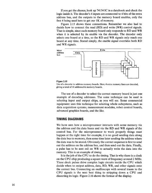
If you get the chance, look up 74154 IC in a databook <strong>and</strong> check the<br />
logic inside it. The decoder's 4 inputs are connected to 4 bits of the extra<br />
address bus, <strong>and</strong>. the outputs to the memory board enables, only the<br />
first 4 being used here to get our lK of memory.<br />
Figure 2.15 shows these connections. Remember we also had to<br />
decide how to connect the read (RD) <strong>and</strong> write (WR) control signals.<br />
That is simple, since each memory board only responds to RD <strong>and</strong> WR<br />
when it is selected by its enable via the decoder. The decoder only<br />
selects one board at a time, so the RD <strong>and</strong> WR signals only reach one<br />
board at any time. Stated simply, the enable signal overrides both RD<br />
<strong>and</strong> WR signals.<br />
16-bit<br />
address<br />
bus<br />
4 bits<br />
8 bits<br />
o<br />
E<br />
C<br />
o<br />
oE<br />
R<br />
t--------+--t-l~<br />
E<br />
Figure 2.15<br />
Use of a decoder to address memory boards. Here, 4 extra memory lines are decoded,<br />
giving a total of 16 addressable memory boards.<br />
The use of a decoder to select the correct memory board is just one<br />
example of decoding addresses. The same technique can be used in<br />
selecting input <strong>and</strong> output chips, as you will see. Some commercial<br />
equipment uses this technique for selecting whole subsystems, such as<br />
data acquisition systems, measurement modules, robot control boards,<br />
advanced graphics boards, <strong>and</strong> the like.<br />
TIMING<br />
DIAGRAMS<br />
We have seen how a microprocessor interacts with some memory via<br />
the address <strong>and</strong> the .data buses <strong>and</strong> via the RD <strong>and</strong> WR signals of the<br />
control bus. For the microprocessor to work properly things must<br />
happen at the right time: for example, it is no good sending data along<br />
the data bus to memory, then some time later sending the address where<br />
the data was to be stored. Obviously the correct sequence is first to send<br />
out the address on the address bus, <strong>and</strong> then send out the data. Finally,<br />
a pulse has to be sent out on WR to actually write the data into the<br />
memory. This is an example of timing.<br />
It is the job of the CPU to do the timing. That is why there is a clock<br />
on the CPU chip producing a square wave of frequency around 2 MHz.<br />
These clock pulses drive complex logic circuits inside the CPU which<br />
decide when to output address, data, RD, WR, <strong>and</strong> other signals onto<br />
the correct bus. Connecting an oscilloscope with several traces to the<br />
CPU signals is the next best thing to stripping down a CPU <strong>and</strong><br />
dissecting its logic. Figure 2.16 shows the format of the display.<br />
16