Microcomputer Circuits and Processes
Microcomputer Circuits and Processes
Microcomputer Circuits and Processes

You also want an ePaper? Increase the reach of your titles
YUMPU automatically turns print PDFs into web optimized ePapers that Google loves.
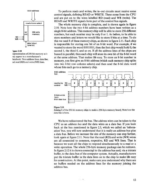
RD<br />
WR<br />
in/<br />
out<br />
8·bit address<br />
row/column<br />
select<br />
256 cells<br />
memory<br />
data in/out<br />
(one bit)<br />
iigure 2.10<br />
~epresentation of 256-bit memory as it<br />
lay appear in a manufacturer's<br />
>atabook. Note address lines, data line,<br />
nd read (RD) <strong>and</strong> write (WR) lines.<br />
To perform reads <strong>and</strong> writes, the in-out circuits must receive some<br />
control signals, defining READ or WRITE. These come from the CPU<br />
<strong>and</strong> are put on to the wires labelled RD (read) <strong>and</strong> WR (write). The<br />
READ <strong>and</strong> WRITE signals form part of the control bus signals.<br />
The whole memory chip is complete, <strong>and</strong> is shown again in figure<br />
2.10. Note how the two 4-bit address numbers have been written as a<br />
single 8-bit address. This memory chip will be able to store 256 different<br />
numbers, but each number may be only 0 or 1. As before, to be able to<br />
store numbers <strong>and</strong> letters we would like to store 8 bits at a time. To do<br />
this we need 8 of these memory chips, as shown in figure 2.11. Each chip<br />
is responsible for storing one bit of an 8-bit word. For example, if we<br />
wanted to store the word 01011011, then the first chip would hold 0, the<br />
second 1, the third 0, <strong>and</strong> so on. If all the address lines of the chips are<br />
bussed in parallel, then each chip will store its own bit of the 8-bit word<br />
at the same address. That makes life easy. To store an 8-bit number in<br />
memory, you first give an 8-bit address (which each memory chip splits<br />
into two 4-bit row--eolumn selects) <strong>and</strong> then send the 8-bit data word<br />
whose bits each go to a memory chip.<br />
8·bit address<br />
bus<br />
read/write<br />
control<br />
RD<br />
WR<br />
8 data wires<br />
form<br />
8-bit data bus<br />
Figure 2.11<br />
Joining 8 of the 256-bit memory chips to make a 256-byte memory boar~. Note how the<br />
data bus is born.<br />
We have rediscovered the bus. The address wires can be taken to the<br />
CPU as an address bus <strong>and</strong> the data wires as a data bus. If you look<br />
back at the bus mentioned in figure 2.5, which we called an 'information'<br />
bus, you will now underst<strong>and</strong> that it is really an address bus plus<br />
a data bus. Before we increase the size of the memory one step further,<br />
look again at figure 2.11. Note that the read (RD) <strong>and</strong> write (WR) wires<br />
are all connected to common, respective, RD <strong>and</strong> WR lines. That is<br />
because we want all the chips to respond simultaneously to a read or a<br />
write operation. The whole 256-byte memory package can be redrawn.<br />
In figure 2.12 it is shown connect~d to the address bus <strong>and</strong>, via a tristate<br />
buffer, to the data bus of the computer system. Actually, manufacturers<br />
put the tristate buffer in the data lines on to the chip to make life easy<br />
for constructors. At this point, make sure you underst<strong>and</strong> why there are<br />
no buffers needed on the address lines for the memory joining the<br />
address bus.<br />
13