Microcomputer Circuits and Processes
Microcomputer Circuits and Processes
Microcomputer Circuits and Processes

You also want an ePaper? Increase the reach of your titles
YUMPU automatically turns print PDFs into web optimized ePapers that Google loves.
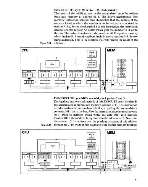
Fifth EXECUTE cycle MOV Acc-+M, clock period 1<br />
The result of the addition, now in the accumulator, must be written<br />
back into memory at address 0111. The 'Move accumulator into<br />
memory' instruction achieves this. Remember that the address of the<br />
memory location where the number is to be written is contained in<br />
register A. So, during clock period 1 of this instruction, the instruction<br />
decoder enables register Ns buffer which puts the number 0111 on to<br />
the bus. The instruction decoder also sends an ALE signal to memory<br />
which latches 0111 into the address latch. Memory location 0111 is now<br />
being addressed. This is the location that will receive the result of the<br />
Figure 3.24 addition.<br />
CPU<br />
MEM<br />
o<br />
o<br />
1 1<br />
o 1<br />
Fifth EXECUTE cycle MOV Acc-+M, clock periods 2 <strong>and</strong> 3<br />
During these last two clock periods of this EXECUTE cycle, the data in<br />
the accumulator is moved into memory location 0111. The instruction<br />
decoder enables the accumulator's buffer, so putting the accumulator's<br />
contents, 1011,on to the bus. Also the instruction decoder sends a write<br />
(WR) pulse to memory which writes the data 1011 into memory<br />
location 0111, this address being stored in the address latch. Note that<br />
the number 1011 is written over the previous occupant of this address,<br />
Figure 3.25 the number 0110, without first having to clear out the memory location.<br />
CPU<br />
MEM<br />
41