Microcomputer Circuits and Processes
Microcomputer Circuits and Processes
Microcomputer Circuits and Processes

You also want an ePaper? Increase the reach of your titles
YUMPU automatically turns print PDFs into web optimized ePapers that Google loves.
amount of decoding in big systems. It has the advantage of looking like<br />
memory to the CPU. Now the CPU spends most of its time shoving<br />
bytes between itself <strong>and</strong> memory. So it does that well: it has many<br />
memory-oriented operations which the user may use in a program. If<br />
input-output looks like memory, then these operations can be applied<br />
also to input-output. Input-output devices which are enabled in this<br />
way are called memory-mapped devices.<br />
Most processors are designed with special input <strong>and</strong> output<br />
facilities so that the input-output circuits are quite separate from<br />
memory. It adds an extra dimension to the computer - ?ften people in<br />
computer laboratories talk about 'memory space' <strong>and</strong> 'input-output<br />
space', referring to that particular region in the high-speed bussed<br />
dimensions of electrical pulses, where memory or in-out signals rule,<br />
respectively. The special input-output facilities involve another control<br />
line. We shall call this line MilO, meaning memory or input-output.<br />
Note the bar above 10; this is consistent with the following definition of<br />
MilO:<br />
MilO = 1 (high)<br />
MilO = 0 (low)<br />
implies a memory type operation<br />
implies an input-output type operation.<br />
For example, if the number 01011110 is put on to the data bus by the<br />
CPU, then it gets sent to memory if MilO = 1, or else to an output<br />
device if MilO = O.<br />
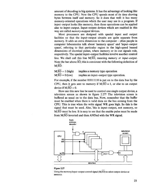
How can this new line be used to control one single output device, a<br />
television screen as shown in figure 2.27? The television screen is<br />
buffered as usual on to the data bus. Now, remember that the buffer<br />
must be enabled when there is valid data on the bus coming from the<br />
CPU. This is true when the write signal WR goes high. So this is the<br />
signal that must be used. Also, 'this is input-output, not memory, so<br />
MilO must be low. It is easy to see that the enable pulse must be made<br />
from MilO inverted <strong>and</strong> then ANDed with the WR signal.<br />
from<br />
address<br />
decoder<br />
CPU<br />
RD t----+----~<br />
WR t----+-----tl....-~<br />
television<br />
screen<br />
D<br />
Figure 2.27<br />
Using the memory/input-output control signal (MjIO) to select output device or<br />
memory.<br />
23