Microcomputer Circuits and Processes
Microcomputer Circuits and Processes
Microcomputer Circuits and Processes

Create successful ePaper yourself
Turn your PDF publications into a flip-book with our unique Google optimized e-Paper software.
D<br />
memory<br />
cell<br />
storing<br />
binary 0<br />
storing<br />
binary 1<br />
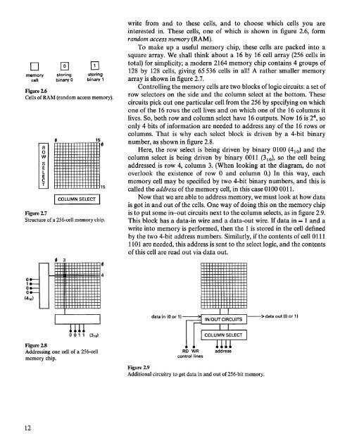
Figure 2.6<br />
Cells of RAM (r<strong>and</strong>om access memory).<br />
R<br />
o<br />
W<br />
S<br />
E<br />
L<br />
E<br />
C<br />
T<br />
I COLUMN SELECT I<br />
Figure 2.7<br />
Structure of a 256-cell memory chip.<br />
.:<br />
f 3<br />
write from <strong>and</strong> to these cells, <strong>and</strong> to choose which cells you are<br />
interested in. These cells, one of which is shown in figure 2.6, form<br />
r<strong>and</strong>om access memory (RAM).<br />
To make up a useful memory chip, these cells are packed into a<br />
square array. We shall think about a 16 by 16 cell array (256 cells in<br />
total) for simplicity; a modern 2164 memory chip contains 4 groups of<br />
128 by 128 cells, giving 65536 cells in all! A rather smaller memory<br />
array is shown in figure 2.7.<br />
Controlling the memory cells are two blocks of logic circuits: a set of<br />
row selectors on the side <strong>and</strong> the column select at the bottom. These<br />
circuits pick out one particular cell from the 256 by specifying on which<br />
one of the 16 rows the cell lives <strong>and</strong> on which one of the 16 columns it<br />
lives. So, both row <strong>and</strong> column select have 16 outputs. Now 16 is 24, so<br />
only 4 bits of information are needed to address any of the 16 rows or<br />
columns. That is why each select block is driven by a 4-bit binary<br />
number, as shown in figure 2.8.<br />
Here, the row select is being driven by binary 0100 (4 10 ) <strong>and</strong> the<br />
column select is being driven by binary 0011 (3 10 ), so the cell being<br />
addressed is row 4, column 3. (When looking at the diagram, do not<br />
overlook the existence of row 0 <strong>and</strong> column 0.) In this way, each<br />
memory cell may be specified by two 4-bit binary numbers, <strong>and</strong> this is<br />
called the address of the memory cell, in this case 0100 001l.<br />
Now that we are able to address memory, we must look at how data<br />
is got in <strong>and</strong> out of the cells. One way of doing this on the memory chip<br />
is to put some in-out circuits next to the column selects, as in figure 2.9.<br />
This block has a data-in wire <strong>and</strong> a data-out wire. If data in = 1 <strong>and</strong> a<br />
write into memory is performed, then the 1 is stored in the cell defined<br />
by the two 4-bit address numbers. Similarly, if the contents of cell 0111<br />
1101 are needed, this address is sent to the select logic, <strong>and</strong> the contents<br />
of this cell are read out via data out.<br />
data in (0 or 1) data out (0 or 1)<br />
Figure 2.8<br />
Addressing one cell of a 256-cell<br />
memory chip.<br />
RD WR<br />
control lines<br />
address<br />
Figure 2.9<br />
Additional circuitry to get data in <strong>and</strong> out of 256-bit memory.<br />
12