Microcomputer Circuits and Processes
Microcomputer Circuits and Processes
Microcomputer Circuits and Processes

You also want an ePaper? Increase the reach of your titles
YUMPU automatically turns print PDFs into web optimized ePapers that Google loves.
Period 2<br />
Period 3<br />
The data bits are put on to the data bus <strong>and</strong> the write (WR) line goes<br />
high. The data bits reach the memory chip, where they are written into<br />
memory as WR is high. They are written in the memory location set up<br />
during Period 1.<br />
By this time, the data has been written into memory <strong>and</strong> so the WR<br />
pulse can go low. That is the end of the operation.<br />
Note how, throughout the entire operation, the address bits were<br />
always there on the bus. That made sure the data went into the correct<br />
memory cell.<br />
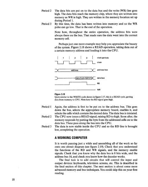
Perhaps just one more example may help you appreciate the beauty<br />
of the system. Figure 2.18 shows a READ operation, taking data out of<br />
a certain memory address <strong>and</strong> loading it into the CPU.<br />
2 3 clock periods<br />
clock<br />
=>< ad_d_re_ss •..••>)-----~(data from memorvC data bus<br />
RD<br />
Figure 2.18<br />
Quite similar to the WRITE cycle shown in figure 2.17, this is a READ cycle, getting<br />
data from memory to CPU. Note how the RD signal goes high.<br />
WR<br />
Period 1<br />
Period 2<br />
Period 3<br />
Again, the address is first to be put on. to the address bus. This goes<br />
down the bus, selects the appropriate memory board, enables it, <strong>and</strong><br />
selects the cells which contain the desired data. The data bus is tristated.<br />
The CPU now issues a READ signal, raising RD to high. Soon after, the<br />
memory responds by putting the byte from the addressed cells on to the<br />
data bus. These pass along the bus into the CPU.<br />
The data is now stable inside the CPU <strong>and</strong> so the RD line is brought<br />
low, completing the operation.<br />
A WORKING<br />
COMPUTER<br />
It is worth pausing just a while <strong>and</strong> assembling all of the work so far<br />
onto one circuit diagram (see figure 2.19). Check that you underst<strong>and</strong><br />
the functions of the RD <strong>and</strong> WR signals, <strong>and</strong> the memory enable<br />
signals. Check that you know why the data bus is 8 bits wide, <strong>and</strong> the<br />
address bus 16, <strong>and</strong> check you know how the decoder works.<br />
The final task is to add circuits that will control the input <strong>and</strong><br />
output devices: keyboards, television screens, etc. This is described in<br />
the final se9tion of this chapter. The next section is about some more<br />
advanced memory <strong>and</strong> bus techniques. You could skip this on your first<br />
reading.<br />
18