INDEX This Index will direct you to explanations of the terms you may look up. Address, 12 Address bus, 13 Address Latch Enable (ALE), 20 Analogue-to-digital conversion (A-to-D), 59 Bits, 11 Bytes, 14 Bubble memory, 47 Bus, 8 . Bus contention, 9 Data bus, 13 Decoder <strong>and</strong> decoding, 15 Digital-to-analogue conversion (D-to-A), 54 Digitizing video pictures, 68 Direct Memory Access (DMA), 68 Dynamic memory, 47 Electrically Eraseable Programmable Read Only Memory (E 2 pROM), 44 Enable <strong>and</strong> enabling, 9 Eraseable Programmable Read Only Memory (EPROM), 44 Execute cycles, 33 Fetch cycles, 33 Flash conversion, 65 Input <strong>and</strong> output, 22, 70 Instruction register, 26 Keyboard interface, 53 Kilobyte (IK), 14 Latch <strong>and</strong> latching, 20 Linear ramp A-to-D convertor, 59 Large-scale integration (LSI), 5 Memory, 11, 44 Memory-mapped input <strong>and</strong> output, 22 M/I0 signal, 23 Mnemonics, 29 Modem, 68 Medium-scale integration (MSI), 5 Multiplexing, 19 Op-code,29 Output <strong>and</strong> input, 22, 70 Program counter, 26, 28 Programmable Read Only Memory (PROM),44 R<strong>and</strong>om Access Memory (RAM), 45 Read (RD) signal, 13 Registers, 26 Read Only Memory (ROM), 44 Serial communication, 67 Seven-segment displays, 50 Successive approximation A-to-D, 62 Timing, 16 Timing diagrams: introduction, 16; output, 42 Very large-scale integration (VLSI), 5 Write (WR) signal, 13 76
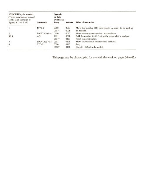
EXECUTE cycle number (These numbers correspond to those in the titles of figures 3.15 to 3.25) Mnemonic Opwcode or data (*indicates data) Address Effect of instruction 2 3&4 5 6 MVI A MOV M~Acc ADI MOV Acc~M STOP 0010 0111 * 0110 1111 0101 * 0111 0000 0110* 0000 0001 0010 0011 0100 0101 0110 0111 Move the number 0111 into register A, ready to be used as an address. Move memory contents into accumulator. Add the number 0101 (5 10 ) to the accumulator, <strong>and</strong> put result in accumulator. Move accumulator contents into memory. Stop. Data 0110 (6 10 ) to be added. (This page may be photocopied for use with the work on pages 34 to 42.)
- Page 2 and 3:
General editor. Revised Nuffield Ad
- Page 4 and 5:
Longman Group Limited Longman House
- Page 6 and 7:
PROLOGUE This Reader explains how m
- Page 8 and 9:
transistor, through the logic circu
- Page 10 and 11:
tasks (large computing 'power'), wa
- Page 12 and 13:
800000 mark. Such high sales result
- Page 14 and 15:
CHAPTER 2 THE ELECTRONICS MICROCOMP
- Page 16 and 17:
enabled, as the truth table in figu
- Page 18 and 19:
D memory cell storing binary 0 stor
- Page 20 and 21:
address bus r----- AND gates RD .--
- Page 22 and 23:
If you get the chance, look up 7415
- Page 24 and 25:
Period 2 Period 3 The data bits are
- Page 26 and 27:
transfers the full 16 bits of addre
- Page 28 and 29:
INPUT AND OUTPUT Devices that input
- Page 30 and 31:
A glance at the timing diagram in f
- Page 32 and 33: CHAPTER 3 RUNNING A SIMPLE PROGRAM
- Page 34 and 35: adding is represented by 1111. Figu
- Page 36 and 37: The number moved into register A im
- Page 38 and 39: loaded into register A. So the CPU
- Page 40 and 41: The FETCH cycles FETCH cycles, whic
- Page 42 and 43: The EXECUTE cycles During EXECUTE c
- Page 44 and 45: Second EXECUTE cycle MOV M--+Acc, c
- Page 46 and 47: Third EXECUTE cycle ADI, clock peri
- Page 48 and 49: That is the end of the program, exc
- Page 50 and 51: CHAPTER 4 MEMORIES, INTERFACES, AND
- Page 52 and 53: measurements made from a microproce
- Page 54 and 55: (al (bl Figure 4.6 (a) Same as in f
- Page 56 and 57: A typical bubble unit contains 300
- Page 58 and 59: (al driver displays 0 1 1 0 1 0 0 1
- Page 60 and 61: Where exactly is this common line c
- Page 62 and 63: this R is in series with the next h
- Page 64 and 65: That is the principle of the conver
- Page 66 and 67: comparator digital-to-analogue data
- Page 68 and 69: II CI l! ~L--~---- desired measurem
- Page 70 and 71: except that it is sent out bit afte
- Page 72 and 73: These equally spaced voltages are f
- Page 74 and 75: Figure 4.35 shows how the letter 'D
- Page 76 and 77: A CONTROL AND DATA AQUISITION COMPU
- Page 78 and 79: It does this by outputting a signal
- Page 80 and 81: The second application, shown in fi